

Features
• One of a Family of 9 Devices with User Memories from 1-Kbit to 256-Kbit
• 128-Kbit (16-Kbyte) EEPROM User Memory
– Sixteen 1-Kbyte (8-Kbit) Zones
– Self-timed Write Cycle
– Single Byte or 128-byte Page Write Mode
– Programmable Access Rights for Each Zone
• 2-Kbit Configuration Zone
– 37-byte OTP Area for User-defined Codes
– 160-byte Area for User-defined Keys and Passwords
• High Security Features
– 64-bit Mutual Authentication Protocol (Under License of ELVA)
– Encrypted Checksum
– Stream Encryption
– Four Key Sets for Authentication and Encryption
– Eight Sets of Two 24-bit Passwords
– Anti-tearing Function
– Voltage and Frequency Monitor
• Smart Card Features
– ISO 7816 Class A (5V) or Class B (3V) Operation
– ISO 7816-3 Asynchronous T = 0 Protocol (Gemplus
– Supports Protocol and Parameters Selection for Faster Operation
– Multiple Zones, Key Sets and Passwords for Multi-application Use
– Synchronous 2-wire Serial Interface for Faster Device Initialization
– Programmable 8-byte Answer-to-reset Register
– ISO 7816-2 Compliant Modules
• Embedded Application Features
– Low Voltage Operation: 2.7V to 5.5V
– Secure Nonvolatile Storage for Sensitive System or User Information
– 2-wire Serial Interface
– 1.0 MHz Compatibility for Fast Operation
– Standard 8-lead Plastic Packages, Green Compliant (exceeds RoHS)
– Same Pinout as 2-wire Serial EEPROMs
• High Reliability
– Endurance: 100,000 Cycles
– Data Retention: 10 years
– ESD Protection: 4,000V min
®
Patent)
CryptoMemory
128 Kbit
AT88SC12816C
Summary
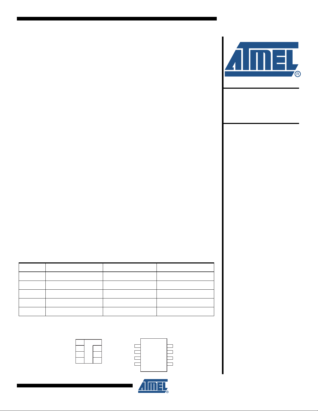
Table 1. Pin Configuration
Pad Description ISO Module Contact Standard Package Pin
VCC Supply Voltage C1 8
GND Ground C5 4
SCL/CLK Serial Clock Input C3 6
SDA/IO Serial Data Input/Output C7 5
RST Reset Input C2 NC
Figure 1. Package Options
Figure 2.
Figure 3.
Smart Card Module
VCC=C1
RST=C2
SCL/CLK=C3
NC=C4
C5=GND
C6=NC
C7=SDA/IO
C8=NC
8-lead SOIC, PDIP
NC
1
NC
2
NC
3
GND
4
VCC
8
NC
7
SCL
6
5
SDA
Note: This is a summary document. A complete document is
available under NDA. For more information, please contact your
local Atmel sales office.
Rev. 5016JS–SMEM–02/09
Description The AT88SC12816C member of the CryptoMemory
ory providing 128 Kbits of user memory with advanced security and cryptographic features built
in. The user memory is divided into 16 1-Kbyte zones, each of which may be individually set with
different security access rights or effectively combined together to provide space for one to sixteen data files.
®
family is a high-performance secure mem-
Smart Card
Applications
Embedded
Applications
The AT88SC12816C provides high security, low cost, and ease of implementation without the
need for a microprocessor operating system. The embedded cryptographic engine provides for
dynamic and symmetric mutual authentication between the device and host, as well as performing stream encryption for all data and passwords exchanged between the device and host. Up to
four unique key sets may be used for these operations. The AT88SC12816C offers the ability to
communicate with virtually any smart card reader using the asynchronous T = 0 protocol (Gemplus Patent) defined in ISO 7816-3. Communication speeds up to 153,600 baud are supported
by utilizing ISO 7816-3 Protocol and Parameter Selection.
Through dynamic and symmetric mutual authentication, data encryption, and the use of
encrypted checksums, the AT88SC12816C provides a secure place for storage of sensitive
information within a system. With its tamper detection circuits, this information remains safe
even under attack. A 2-wire serial interface running at 1.0 MHz is used for fast and efficient communications with up to 15 devices that may be individually addressed. The AT88SC12816C is
available in industry standard 8-lead packages with the same familiar pinout as 2-wire serial
EEPROMs.
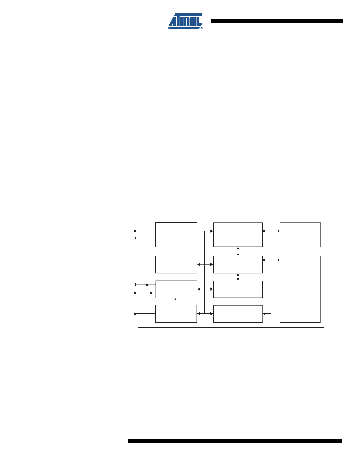
Figure 2. Block Diagram
VCC
GND
Power
Management
Synchronous
Interface
Authentication,
Encryption and
Certification Unit
Data Transfer
Random
Generator
SCL/CLK
SDA/IO
RST
Asynchronous
ISO Interface
Reset Block
Password
Verification
Answer to Reset
EEPROM
Pin
Descriptions
Supply Voltage (VCC) The VCC input is a 2.7V to 5.5V positive voltage supplied by the host.
Clock (SCL/CLK) In the asynchronous T = 0 protocol, the SCL/CLK input is used to provide the device with a car-
rier frequency f. The nominal length of one bit emitted on I/O is defined as an “elementary time
unit” (ETU) and is equal to 372/f. When the synchronous protocol is used, the SCL/CLK input is
used to positive edge clock data into the device and negative edge clock data out of the device.
2
AT88SC12816C
5016JS–SMEM–02/09

AT88SC12816C
Reset (RST) The AT88SC12816C provides an ISO 7816-3 compliant asynchronous answer to reset
sequence. When the reset sequence is activated, the device will output the data programmed
into the 64-bit answer-to-reset register. An internal pull-up on the RST input pad allows the
device to be used in synchronous mode without bonding RST. The AT88SC12816C does not
support the synchronous answer-to-reset sequence.
Serial Data
(SDA/IO)
The SDA pin is bidirectional for serial data transfer. This pin is open-drain driven and may be
wired with any number of other open drain or open collector devices. An external pull-up resistor
should be connected between SDA and V
. The value of this resistor and the system capaci-
CC
tance loading the SDA bus will determine the rise time of SDA. This rise time will determine the
maximum frequency during read operations. Low value pull-up resistors will allow higher frequency operations while drawing higher average power. SDA/IO information applies to both
asynchronous and synchronous protocols.
When the synchronous protocol is used, the SCL/CLK input is used to positive edge clock data
into the device and negative edge clock data out of the device.
Table 2. DC Characteristics
Applicable over recommended operating range from VCC = +2.7 to 5.5V, TAC = -40oC to +85oC (unless otherwise noted)
Symbol Parameter Test Condition Min Typ Max Units
(2)
V
CC
I
CC
I
CC
I
CC
I
CC
I
SB
(1)
V
IL
(1)
V
IL
(1)
V
IL
(1)(2)
V
IH
(1)(2)
V
IH
(1)(2)
V
IH
I
IL
I
IL
I
IL
I
IH
I
IH
I
IH
V
OH
V
OL
I
OH
Notes: 1. VIL min and VIH max are reference only and are not tested.
Supply Voltage 2.7 5.5 V
Supply Current (VCC = 5.5V) Async READ at 3.57MHz 5 mA
Supply Current (VCC = 5.5V) Async WRITE at 3.57MHz 5 mA
Supply Current (VCC = 5.5V) Synch READ at 1MHz 5 mA
Supply Current (VCC = 5.5V) Synch WRITE at 1MHz 5 mA
Standby Current (VCC = 5.5V) VIN = VCC or GND 1 mA
SDA/IO Input Low Threshold 0 VCC x 0.2 V
SCL/CLK Input Low Threshold 0 VCC x 0.2 V
RST Input Low Threshold 0 VCC x 0.2 V
SDA/IO Input High Threshold VCC x 0.7 V
SCL/CLK Input High Threshold VCC x 0.7 V
RST Input High Threshold VCC x 0.7 V
SDA/IO Input Low Current 0 < V
SCL/CLK Input Low Current 0 < V
RST Input Low Current 0 < V
SDA/IO Input High Current VCC x 0.7 < VIH < V
SCL/CLK Input High Current VCC x 0.7 < VIH < V
RST Input High Current VCC x 0.7 < VIH < V
< VCC x 0.15 15 uA
IL
< VCC x 0.15 15 uA
IL
< VCC x 0.15 50 uA
IL
CC
CC
CC
20 uA
100 uA
150 uA
SDA/IO Output High Voltage 20K ohm external pull-up VCC x 0.7 V
CC
CC
CC
CC
SDA/IO Output Low Voltage IOL = 1mA 0 VCC x 0.15 V
SDA/IO Output High Current V
OH
20 uA
2. To prevent Latch Up Conditions from occurring during Power Up of the AT88SCxxxxC, Vcc must be turned on before applying Vih. For Powering Down, Vih must be removed before turning vcc off.
V
V
V
V
5016JS–SMEM–02/09
3

Table 3. AC Characteristics
Applicable over recommended operating range from VCC = +2.7 to 5.5V,
= -40oC to +85oC, CL = 30pF (unless otherwise noted)
T
AC
Symbol Parameter Min Max Units
f
CLK
f
CLK
f
CLK
t
t
t
t
t
AA
t
HD.STA
t
SU.STA
t
HD.DAT
t
SU.DAT
t
SU.STO
t
DH
t
WR
t
WR
Async Clock Frequency (VCC Range: +4.5 - 5.5V) 1 5 MHz
Async Clock Frequency (VCC Range: +2.7 - 3.3V) 1 4 MHz
Synch Clock Frequency 0 1 MHz
Clock Duty cycle 40 60 %
Rise Time - I/O, RST 1 uS
R
Fall Time - I/O, RST 1 uS
F
Rise Time - CLK 9% x period uS
R
Fall Time - CLK 9% x period uS
F
Clock Low to Data Out Valid 35 nS
Start Hold Time 200 nS
Start Set-up Time 200 nS
Data In Hold Time 10 nS
Data In Set-up Time 100 nS
Stop Set-up Time 200 nS
Data Out Hold Time 20 nS
Write Cycle Time (at 20⋅ C) 5 mS
Write Cycle Time (-40o to +85oC) 7 mS
Device
Operation For
Synchronous
Protocols
CLOCK and DATA TRANSITIONS: The SDA pin is normally pulled high with an external device.
Data on the SDA pin may change only during SCL low time periods (see Figure 5 on page 5).
Data changes during SCL high periods will indicate a start or stop condition as defined below.
START CONDITION: A high-to-low transition of SDA with SCL high is a start condition which
must precede any other command (see Figure 6 on page 6).
STOP CONDITION: A low-to-high transition of SDA with SCL high is a stop condition. After a
read sequence, the stop command will place the EEPROM in a standby power mode (see Fig-
ure 6 on page 6).
ACKNOWLEDGE: All addresses and data words are serially transmitted to and from the
EEPROM in 8-bit words. The EEPROM sends a zero to acknowledge that it has received each
word. This happens during the ninth clock cycle.
MEMORY RESET: After an interruption in protocol, power loss or system reset, any 2-wire part
can be reset by following these steps:
1. Clock up to 9 cycles.
2. Look for SDA high in each cycle while SCL is high.
3. Create a start condition.
4
AT88SC12816C
5016JS–SMEM–02/09
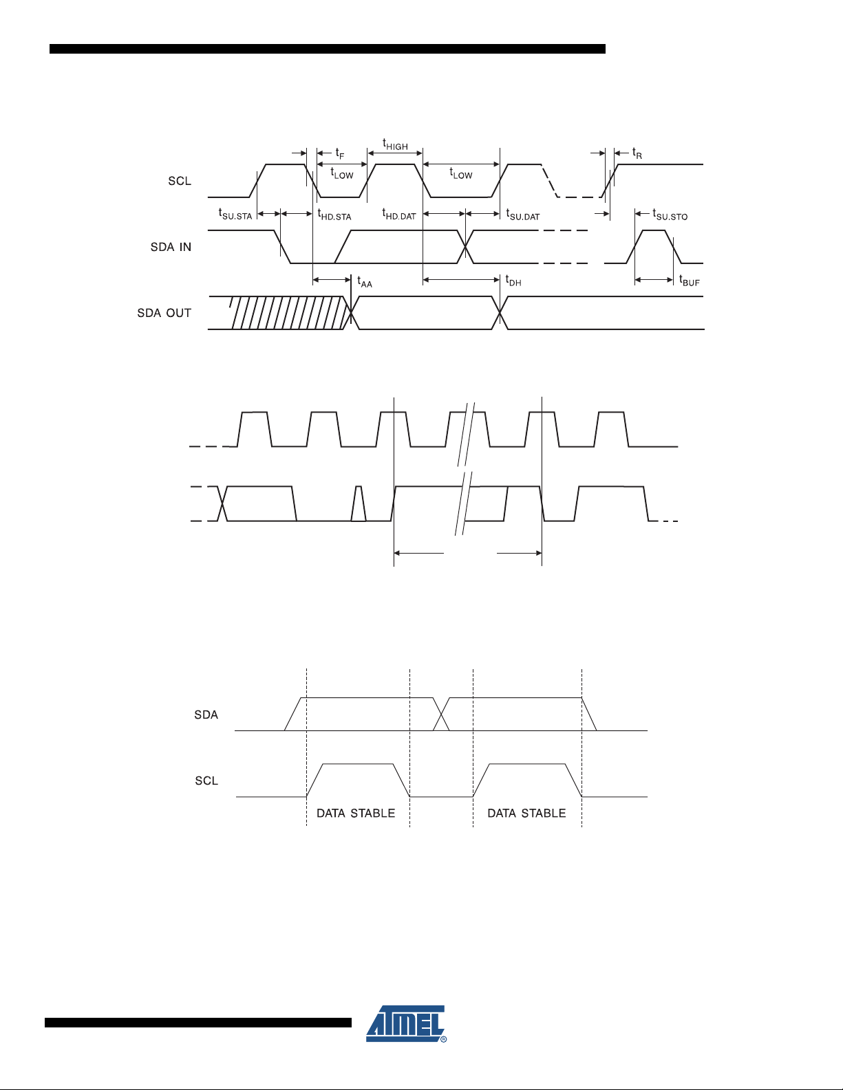
Figure 3. Bus Timing for 2 wire communications
SCL: Serial Clock, SDA: Serial Data I/O
Figure 4. Write Cycle Timing:
SCL: Serial Clock, SDA: Serial Data I/O
SCL
AT88SC12816C
SDA
Figure 5. Data Validity
8th BIT
WORDn
Note: The write cycle time tWR is the time from a valid stop condition of a write sequence to the end of
the internal clear/write cycle.
ACK
STOP
CONDITION
CHANGE
ALLOWED
DATA
(1)
t
WR
START
CONDITION
5016JS–SMEM–02/09
5
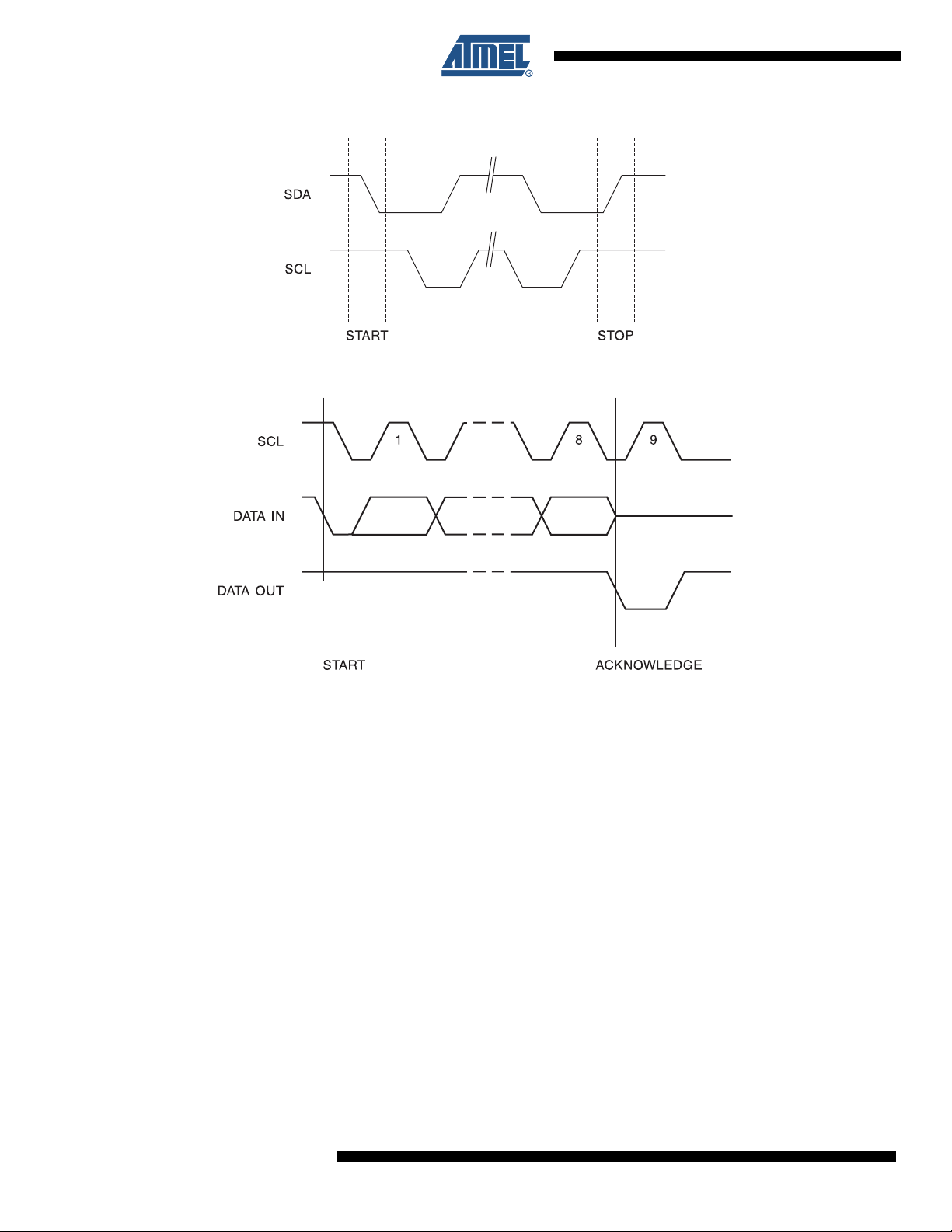
Figure 6. Start and Stop Definitions
Figure 7. Output Acknowledge
Device
Architecture
User Zones The EEPROM user memory is divided into 16 zones of 8,192 bits each. Multiple zones allow for
different types of data or files to be stored in different zones. Access to the user zones is allowed
only after security requirements have been met. These security requirements are defined by
theuser during the personalization of the device in the configuration memory. If the same security requirements are selected for multiple zones, then these zones may effectively be accessed
as one larger zone.
6
AT88SC12816C
5016JS–SMEM–02/09

AT88SC12816C
Figure 8. User Zone
ZONE $0 $1 $2 $3 $4 $5 $6 $7
$000
User 0
User 1 $000
--
-
--
User 14 $3F8
User 15
- 1024 Bytes
-
$3F8
$000
- 1024 Bytes
-
$3F8
Control Logic Access to the user zones occurs only through the control logic built into the device. This logic is
configurable through access registers, key registers and keys programmed into the configuration
memory during device personalization. Also implemented in the control logic is a cryptographic
engine for performing the various higher-level security functions of the device.
Configuration
Memory
The configuration memory consists of 2048 bits of EEPROM memory used for storing passwords, keys and codes and for defining security levels to be used for each user zone. Access
rights to the configuration memory are defined in the control logic and may not be altered by the
user.
5016JS–SMEM–02/09
7

Figure 9. Configuration Memory
$0 $1 $2 $3 $4 $5 $6 $7
$00 Answer To Reset
$08 Fab Code MTZ Card Manufacturer Code
$10 Lot History Code Read Only
$18 DCR Identification Number Nc
$20 AR0 PR0 AR1 PR1 AR2 PR2 AR3 PR3
$28 AR4 PR4 AR5 PR5 AR6 PR6 AR7 PR7
$30 AR8 PR8 AR9 PR9 AR10 PR10 AR11 PR11
$38 AR12 PR12 AR13 PR13 AR14 PR14 AR15 PR15
$40
Issuer Code
$48
$50
$58
$60
Identification
Access Control
$68
For Authentication and Encryption use Cryptography
$70
$78
$80
$88
$90
$98
For Authentication and Encryption use Secret
$A0
$A8
$B0 PAC Write 0 PAC Read 0
$B8 PAC Write 1 PAC Read 1
$C0 PAC Write 2 PAC Read 2
$C8 PAC Write 3 PAC Read 3
$D0 PAC Write 4 PAC Read 4
$D8 PAC Write 5 PAC Read 5
$E0 PAC Write 6 PAC Read 6
$E8 PAC Write 7 PAC Read 7
$F0
Reserved Forbidden
$F8
Password
8
AT88SC12816C
5016JS–SMEM–02/09

AT88SC12816C
Security Fuses There are three fuses on the device that must be blown during the device personalization pro-
cess. Each fuse locks certain portions of the configuration memory as OTP memory. Fuses are
designed for the module manufacturer, card manufacturer and card issuer and should be blown
in sequence, although all programming of the device and blowing of the fuses may be performed
at one final step.
Protocol
Selection
Asynchronous
T = 0 Protocol
The AT88SC12816C supports two different communication protocols.
• Smart Card Applications: The asynchronous T = 0 protocol defined by ISO 7816-3 is used
for compatibility with the industry’s standard smart card readers.
• Embedded Applications: A 2-wire serial interface is used for fast and efficient
communication with logic or controllers.
The power-up sequence determines which of the two communication protocols will be used.
This power-up sequence complies with ISO 7816-3 for a cold reset in smart card applications.
•V
• Set I/O-SDA in receive mode.
• Provide a clock signal to CLK-SCL.
• RST goes high after 400 clock cycles.
The device will respond with a 64-bit ATR code, including historical bytes to indicate the memory
density within the CryptoMemory family. Once the asynchronous mode has been selected, it is
not possible to switch to the synchronous mode without powering off the device.
Figure 10. Asynchronous T = 0 Protocol (Gemplus Patent)
goes high; RST, I/O-SDA and CLK-SCL are low.
CC
V
cc
I/O-SDA
RST
AT R
Synchronous
2-wire Serial
Interface
5016JS–SMEM–02/09
CLK-SCL
After a successful ATR, the Protocol and Parameter Selection (PPS) protocol, as defined by ISO
7816-3, may be used to negotiate the communications speed with CryptoMemory devices 32
Kbits and larger. CryptoMemory supports D values of 1, 2, 4, 8, 12, and 16 for an F value of 372.
Also supported are D values of 8 and 16 for F = 512. This allows selection of 8 communications
speeds ranging from 9600 baud to 153,600 baud.
The synchronous mode is the default after powering up VCC due to an internal pull-up on RST.
For embedded applications using CryptoMemory in standard plastic packages, this is the only
communication protocol.
• Power-up V
• After stable V
, RST goes high also.
CC
, CLK-SCL and I/O-SDA may be driven.
CC
9

Figure 11. Synchronous 2-wire Protocol
V
cc
I/O-SDA
RST
1
CLK-SCL
Note: Five clock pulses must be sent before the first command is issued.
2
3
45
Communication
Security Modes
Table 4. Communication Security Modes
Mode Configuration Data User Data Passwords Data Integrity Check
Standard Clear Clear Clear MDC
Authentication Clear Clear Encrypted MAC
Encryption Clear Encrypted Encrypted MAC
Note: 1. Configuration data include viewable areas of the Configuration Zone except the passwords:
MDC: Modification Detection Code
MAC: Message Authentication Code.
Communications between the device and host operate in three basic modes. Standard mode is
the default mode for the device after power-up. Authentication mode is activated by a successful
authentication sequence. Encryption mode is activated by a successful encryption activation following a successful authentication.
(1)
Security
Options
Anti-tearing In the event of a power loss during a write cycle, the integrity of the device’s stored data may be
recovered. This function is optional: the host may choose to activate the anti-tearing function,
depending on application requirements. When anti-tearing is active, write commands take longer
to execute, since more write cycles are required to complete them, and data are limited to eight
bytes.
Data are written first to a buffer zone in EEPROM instead of the intended destination address,
but with the same access conditions. The data are then written in the required location. If this
second write cycle is interrupted due to a power loss, the device will automatically recover the
data from the system buffer zone at the next power-up.
In 2-wire mode, the host is required to perform ACK polling for up to 8 ms after write commands
when anti-tearing is active. At power-up, the host is required to perform ACK polling, in some
cases for up to 2 ms, in the event that the device needs to carry out the data recovery process.
Write Lock If a user zone is configured in the write lock mode, the lowest address byte of an 8-byte page
constitutes a write access byte for the bytes of that page.
Example: The write lock byte at $080 controls the bytes from $080 to $087.
10
AT88SC12816C
5016JS–SMEM–02/09

AT88SC12816C
Figure 12. Write Lock Example
Address$0$1$2$3$4$5$6$7
$080 11011001 xxxx xxxx xxxx xxxx xxxx xxxx xxxx xxxx xxxx xxxx xxxx xxxx xxxx xxxx
locked locked locked
The write lock byte may also be locked by writing its least significant (rightmost) bit to “0”. Moreover, when write lock mode is activated, the write lock byte can only be programmed – that is,
bits written to “0” cannot return to “1”.
In the write lock configuration, only one byte can be written at a time. Even if several bytes are
received, only the first byte will be taken into account by the device.
Password
Verification
Authentication
Protocol
Passwords may be used to protect read and/or write access of any user zone. When a valid
password is presented, it is memorized and active until power is turned off, unless a new password is presented or RST becomes active. There are eight password sets that may be used to
protect any user zone. Only one password is active at a time, but write passwords give read
access also.
The access to a user zone may be protected by an authentication protocol. Any one of four keys
may be selected to use with a user zone.
The authentication success is memorized and active as long as the chip is powered, unless a
new authentication is initialized or RST becomes active. If the new authentication request is not
validated, the card loses its previous authentication and it should be presented again. Only the
last request is memorized.
Note: Password and authentication may be presented at any time and in any order. If the trials limit has
been reached (after four consecutive incorrect attempts), the password verification or authentication process will not be taken into account.
Figure 13. Password and Authentication Operations
5016JS–SMEM–02/09
VERIFY RPW
DATA
Checksum (CS)
VERIFY CS
Write DATA
VERIFY CS
CS
11

Checksum The AT88SC12816C implements a data validity check function in the form of a checksum, which
may function in standard, authentication or encryption modes.
In the standard mode, the checksum is implemented as a Modification Detection Code (MDC), in
which the host may read a MDC from the device in order to verify that the data sent was
received correctly.
In the authentication and encryption modes, the checksum becomes more powerful since it provides a bidirectional data integrity check and data origin authentication capability in the form of a
Message Authentication Code (MAC). Only the host/device that carried out a valid authentication is capable of computing a valid MAC. While operating in the authentication or encryption
modes, the use of a MAC is required. For an ongoing command, if the device calculates a MAC
different from the MAC transmitted by the host, not only is the command abandoned but the
mode is also reset. A new authentication and/or encryption activation will be required to reactivate the MAC.
Encryption The data exchanged between the device and the host during read, write and verify password
commands may be encrypted to ensure data confidentiality.
The issuer may choose to require encryption for a user zone by settings made in the configuration memory. Any one of four keys may be selected for use with a user zone. In this case,
activation of the encryption mode is required in order to read/write data in the zone and only
encrypted data will be transmitted. Even if not required, the host may elect to activate encryption
provided the proper keys are known.
Supervisor Mode Enabling this feature allows the holder of one specific password to gain full access to all eight
password sets, including the ability to change passwords.
Modify Forbidden No write access is allowed in a user zone protected with this feature at any time. The user zone
must be written during device personalization prior to blowing the security fuses.
Program Only For a user zone protected by this feature, data within the zone may be changed from a “1” to a
“0”, but never from a “0” to a “1”.
Initial Device
Programming
To enable the security features of CryptoMemory, the device must first be personalized to set up
several registers and load in the appropriate passwords and keys. This is accomplished through
programming the configuration memory of CryptoMemory using simple write and read commands. To gain access to the configuration memory, the secure code must first be successfully
presented. For the AT88SC12816C device, the secure code is $22 EF 67. After writing and verifying data in the configuration memory, the security fuses must be blown to lock this information
in the device. For additional information on personalizing CryptoMemory, please see the application notes Programming CryptoMemory for Embedded Applications and Initializing
CryptoMemory for Smart Card Applications (at www.Atmel.com).
12
AT88SC12816C
5016JS–SMEM–02/09

AT88SC12816C
Ordering Information
Ordering Code Package Voltage Range Temperature Range
AT88SC12816C-MJ M2 – J Module 2.7V–5.5V Commercial (0°C–70°C)
AT88SC12816C-PU
AT88SC12816C-SU
AT88SC12816C-WI 7 mil wafer 2.7V–5.5V Industrial (−40°C–85°C)
Package Type
M2 – J Module M2 ISO 7816 Smart Card Module
8P3 8-lead, 0.300” Wide, Plastic Dual Inline Package (PDIP)
8S1 8-lead, 0.150” Wide, Plastic Gull Wing Small Outline Package (JEDEC SOIC)
Note: 1. Formal drawings may be obtained from an Atmel sales office.
(1)
8P3
8S1
Description
2.7V–5.5V
Green compliant (exceeds
RoHS)/Industrial (−40°C–85°C)
5016JS–SMEM–02/09
13

Packaging Information
Ordering Code: MJ
Module Size: M2
Dimension*: 12.6 x 11.4 [mm]
Glob Top: Round - 8.5 [mm]
Thickness: 0.58 [mm]
Pitch: 14.25 mm
*Note: The module dimensions listed refer to the dimensions of the exposed metal contact area. The actual dimensions
of the module after excise or punching from the carrier tape are generally 0.4 mm greater in both directions
(i.e., a punched M2 module will yield 13.0 x 11.8 mm).
14
AT88SC12816C
5016JS–SMEM–02/09

Ordering Code: SU
Ø
E
1
N
TOP VIEW
C
E1
A
b
L
A1
e
D
SIDE VIEW
8-lead SOIC
AT88SC12816C
C
1
E
E1
L
TOP VIEW
N
Ø
END VIEW
e
D
SIDE VIEW
b
A
A1
SYMBOL
A 1.35 – 1.75
A1 0.10 – 0.25
b 0.31 – 0.51
C 0.17 – 0.25
D 4.80 – 5.05
E1 3.81 – 3.99
E 5.79 – 6.20
e 1.27 BSC
L 0.40 – 1.27
θ 0° – 8°
COMMON DIMENSIONS
(Unit of Measure = mm)
MIN
NOM
MAX
NOTE
Note:
These drawings are for general information only. Refer to JEDEC Drawing MS-012, Variation AA for proper dimensions, tolerances, datums, etc.
1150 E. Cheyenne Mtn. Blvd.
Colorado Springs, CO 80906
R
5016JS–SMEM–02/09
TITLE
8S1, 8-lead (0.150" Wide Body), Plastic Gull Wing
Small Outline (JEDEC SOIC)
DRAWING NO.
8S1 C
3/17/05
REV.
15

Ordering Code: PU
8-lead PDIP
D1
b3
4 PLCS
Top View
D
e
Side View
1
E
E1
N
c
eA
End View
COMMON DIMENSIONS
(Unit of Measure = inches)
b
b2
A2 A
SYMBOL
A 0.210 2
A2 0.115 0.130 0.195
b 0.014 0.018 0.022 5
b2 0.045 0.060 0.070 6
b3 0.030 0.039 0.045 6
c 0.008 0.010 0.014
D 0.355 0.365 0.400 3
L
D1 0.005 3
E 0.300 0.310 0.325 4
E1 0.240 0.250 0.280 3
e 0.100 BSC
eA 0.300 BSC 4
L 0.115 0.130 0.150 2
MIN
NOM
MAX
NOTE
Notes: 1. This drawing is for general information only; refer to JEDEC Drawing MS-001, Variation BA for additional information.
16
2. Dimensions A and L are measured with the package seated in JEDEC seating plane Gauge GS-3.
3. D, D1 and E1 dimensions do not include mold Flash or protrusions. Mold Flash or protrusions shall not exceed 0.010 inch.
4. E and eA measured with the leads constrained to be perpendicular to datum.
5. Pointed or rounded lead tips are preferred to ease insertion.
6. b2 and b3 maximum dimensions do not include Dambar protrusions. Dambar protrusions shall not exceed 0.010 (0.25 mm).
TITLE
2325 Orchard Parkway
R
San Jose, CA 95131
8P3, 8-lead, 0.300" Wide Body, Plastic Dual
In-line Package (PDIP)
AT88SC12816C
DRAWING NO.
8P3
5016JS–SMEM–02/09
01/09/02
REV.
B

Revision History
AT88SC12816C
Doc. Rev. Date Comments
5016JS 02/09 Features Section – add ‘Green compliant (exceeds RoHS) to
end of ‘Standard 8-lead Plastic Packages’ bullet
added Note to DC Characteristics table and applied to Vcc
and all 3 instances of Vih symbols in table.
Ordering Information page: Add ‘Green compliant (exceeds
RoHS) to middle row of Temperature Range
Replace ‘Lead-free/Halogen-free. Keep industrial
Updated to 2009 Copyright.
5016IS 1/2009 Removed P module offering.
5016HS 11/2008 Updated timing diagrams.
5016GS 4/14/07 Final release version.
5016GS 1/26/07 Replaced User Zone, Configuration Memory, and Write Lock
Example tables with new information.
5016GS 1/2007 Implemented revision history.
Removed Industrial package offerings.
Removed 8Y4 package offering.
5016JS–SMEM–02/09
17

Headquarters International
Atmel Corporation
2325 Orchard Parkway
San Jose, CA 95131
USA
Tel: 1(408) 441-0311
Fax: 1(408) 487-2600
Atmel Asia
Room 1219
Chinachem Golden Plaza
77 Mody Road Tsimshatsui
East Kowloon
Hong Kong
Tel: (852) 2721-9778
Fax: (852) 2722-1369
Product Contact
Web Site
www.atmel.com
Literature Requests
www.atmel.com/literature
Atmel Europe
Le Krebs
8, Rue Jean-Pierre Timbaud
BP 309
78054 Saint-Quentin-enYvelines Cedex
France
Tel: (33) 1-30-60-70-00
Fax: (33) 1-30-60-71-11
Technical Support
securemem@atmel.com
Atmel Japan
9F, Tonetsu Shinkawa Bldg.
1-24-8 Shinkawa
Chuo-ku, Tokyo 104-0033
Japan
Tel: (81) 3-3523-3551
Fax: (81) 3-3523-7581
Sales Contact
www.atmel.com/contacts
Disclaimer: The information in this document is provided in connection with Atmel products. No license, express or implied, by estoppel or otherwise, to any
intellectual property right is granted by this document or in connection with the sale of Atmel products. EXCEPT AS SET FORTH IN ATMEL’S TERMS AND CONDI-
TIONS OF SALE LOCATED ON ATMEL’S WEB SITE, ATMEL ASSUMES NO LIABILITY WHATSOEVER AND DISCLAIMS ANY EXPRESS, IMPLIED OR STATUTORY
WARRANTY RELATING TO ITS PRODUCTS INCLUDING, BUT NOT LIMITED TO, THE IMPLIED WARRANTY OF MERCHANTABILITY, FITNESS FOR A PARTICULAR
PURPOSE, OR NON-INFRINGEMENT. IN NO EVENT SHALL ATMEL BE LIABLE FOR ANY DIRECT, INDIRECT, CONSEQUENTIAL, PUNITIVE, SPECIAL OR INCIDENTAL DAMAGES (INCLUDING, WITHOUT LIMITATION, DAMAGES FOR LOSS OF PROFITS, BUSINESS INTERRUPTION, OR LOSS OF INFORMATION) ARISING OUT OF
THE USE OR INABILITY TO USE THIS DOCUMENT, EVEN IF ATMEL HAS BEEN ADVISED OF THE POSSIBILITY OF SUCH DAMAGES. Atmel makes no
representations or warranties with respect to the accuracy or completeness of the contents of this document and reserves the right to make changes to specifications
and product descriptions at any time without notice. Atmel does not make any commitment to update the information contained herein. Unless specifically provided
otherwise, Atmel products are not suitable for, and shall not be used in, automotive applications. Atmel’s products are not intended, authorized, or warranted for use
as components in applications intended to support or sustain life.
© 2009 Atmel Corporation. All rights reserved. Atmel®, Atmel logo and combinations thereof, CryptoMemory® and others, are registered
trademarks or trademarks of Atmel Corporation or its subsidiaries. Other terms and product names may be trademarks of others.
5016JS–SMEM–02/09
 Loading...