

Page 1
MagniVu™Acquisition Technology
Provides 500 ps Timing Resolution on
All Channels All the Time Through a
Single Probe
Up to 200 MHz State Acquisition with
400 MHz Data Rate Supports Advanced
Processors and Buses
Simultaneous State and High Speed
Timing Analysis Through the Same
Probes Pinpoints Elusive Integration
Faults
64 Channel Pattern Generator with up
to 268 MHz and up to 2 MB Memory
Depth Provides Digital Stimulus for
Functional Verification, Debugging and
Stress Testing
Four Channel Digitizing Oscilloscope
with up to 1 GHz, 5 GS/s Provides Highfidelity Signal Quality Measurements of
Digital Signals
Expansion Mainframe Supports up to 16
Modules with up to 2,176 LA channels,
1,024 Pattern Generator Channels or 64
Digitizing Oscilloscope channels for
Large, Multiple Processor and Bus
Applications
Microsoft
®
Windows®-based PC
Platform Provides Familiar User
Interface With Network Connectivity
Hardware Debug and Verification
Processor/Bus Debug and Verification
Embedded Software Integration, Debug
and Verification
Embedded Real-time Software
Optimization
System Validation
BREAKTHROUGH SOLUTIONS FOR REAL-TIME
DIGITAL SYSTEMS ANALYSIS
Today’s digital design engineers face daily pressures
to speed new products to the marketplace. The
TLA 700 Series answers the need with breakthrough
solutions for the entire design team, providing the
ability to quickly monitor, capture and analyze realtime system operation in order to debug, verify,
optimize and validate digital systems.
Features and Benefits Applications
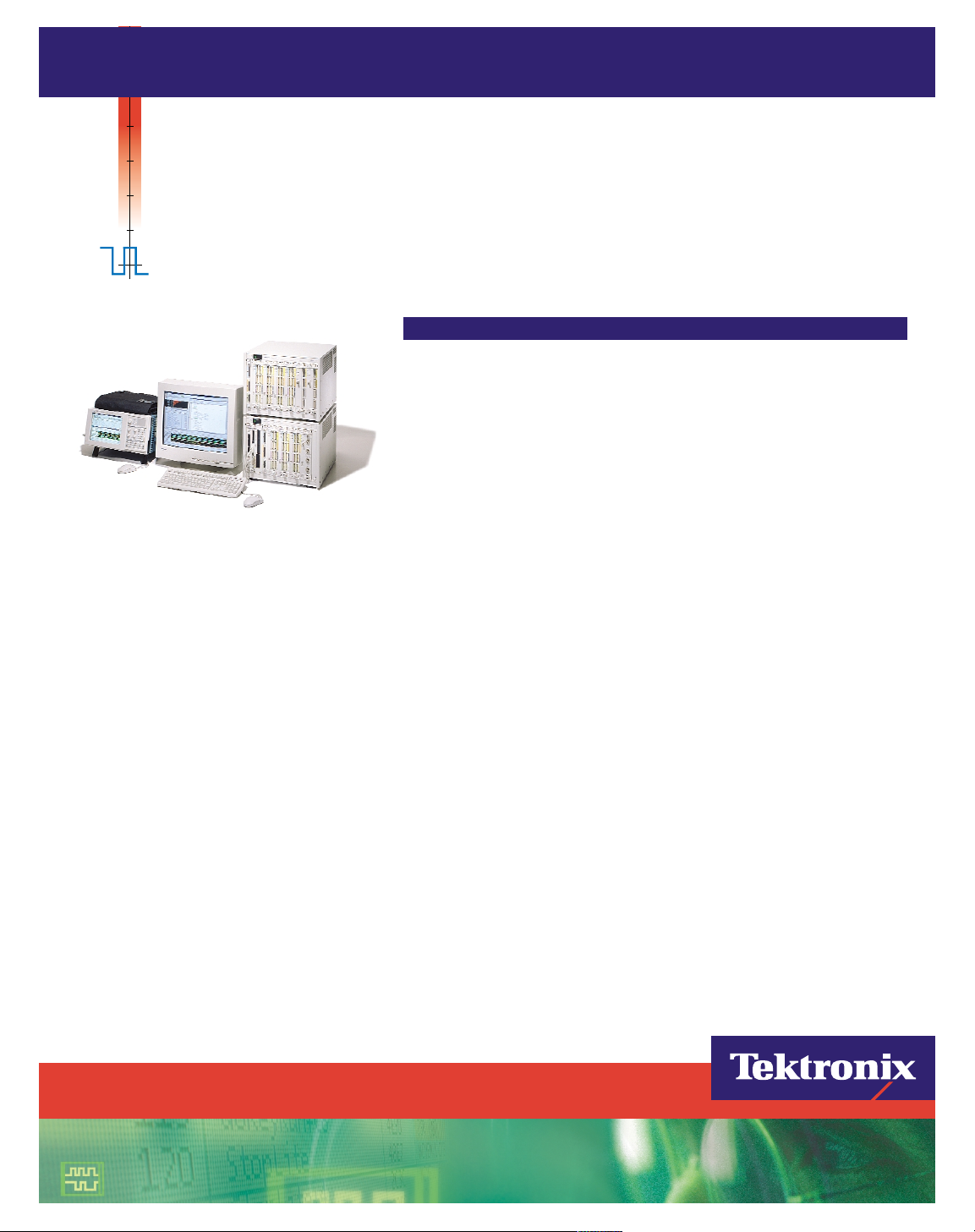
Logic Analyzers
TLA 700 Series
®
Page 2

LOGIC ANALYZERS • TLA 700 SERIES
2
Logic Analyzer Modules
GENERAL
Number of Channels per Module (all channels are acquired including clocks) –
TLA 7N1: 34 channels (2 are clock/qualifier
channels).
TLA 7N2, TLA 7P2: 68 channels (4 are clock/
qualifier channels).
TLA 7N3: 102 channels (4 are clock/qualifier and
2 are qualifier channels).
TLA 7N4, TLA 7P4: 136 channels (4 are
clock/qualifier and 4 are qualifier channels).
Channel Grouping – No limit to number of
groups or number of channels per group (all
channels can be reused in multiple groups).
Module “Merging” – Three 102 channel or 136
channel modules can be “merged” to make up to
a 408 channel module. Merged modules exhibit
the same depth as the lesser of the three individual modules. Word/range/setup-andhold/glitch/transition recognizers span all three
modules. Only one set of clock connections is
required.
Time Stamp – 50 Bits at 500 ps resolution (6.5
day range).
Clocking/Acquisition Modes- State, timing,
simultaneous.
Number of Mainframe Slots Required – 2.
INPUT CHARACTERISTICS (WITH P6417,
P6418 OR P6434 PROBES)
Capacitive Loading –
1.4 pF typical data; 2pF typical clock (P6418).
2 pF typical (P6417 & P6434).
Threshold Selection Range – From +5.0 V
to –2.0 V in 50 mV increments.
Threshold Selection Channel Granularity –
Separate selection for clock (1) and data (16) for
each 17 channel probe connector.
Threshold Accuracy (including probe) –
±100 mV.
Input Voltage Range –
Operating: 6.5 V
P-P
centered around the programmed threshold.
Non-destructive: ±15 V.
Input Signal Swing (probe overdrive) –
±250 mV or ±25% of signal swing, whichever is
greater (P6417 & P6418).
±300 mV or ± 25% of signal swing (P6434).
Input Signal Minimum Slew Rate –
200 mV/ns typical.
STATE ACQUISITION CHARACTERISTICS
(WITH P6417, P6418 OR P6434 PROBES)
Maximum Synchronous Clock Rate –
100M Hz standard, 200 M Hz optional.
Maximum Data Rate (Half Channels) –
400 MHz, typical. Requires 200 MHz state option.
State Memory Depth – 64 K, 256 K, 1 M, 4 M
or 16M bits per channel.
Setup Time Selection Range – From 8.5 ns
before, to 7.0 ns after clock edge.
Setup-and-hold Window – 2.0 ns typical.
Minimum Clock Pulse Width – 2 ns.
Active Clock Edge Separation – 5 ns.
Demux Channel Selection – 32 channels can
be demultiplexed to other channels through user
interface; for all channels contact local Tektronix
account manager.
TIMING ACQUISITION CHARACTERISTICS
(WITH P6417, P6418 OR P6434 PROBES)
Main Timing Resolution – 4 ns to 50 ms.
Main Timing Resolution with Glitch Storage
Enabled – 10 ns to 50 ms.
Main Timing Memory Depth (with or without transitional storage enabled) – 64 K,
256 K, 1 M, 4 M or 16M bits per channel.
Main Timing Memory Depth with Glitch
Storage Enabled – Half of default main
memory depth.
MagniVu – 500 ps.
MagniVu Timing Memory Depth – 2 Kbits
(2048) per channel.
Channel-to-channel Skew – ≤1 ns typical.
Minimum Recognizable Pulse Width (single
channel) – 2 ns.
Minimum Recognizable Glitch Width (single
channel) – 2 ns.
Minimum Recognizable Multi-channel
Trigger Event – Sample period + 2 ns.
TRIGGER CHARACTERISTICS
Independent Trigger States – 16.
Maximum Independent If/then Clauses per
State – 16.
Maximum Number of Events per If/then
Clause – 8.
Maximum Number of Actions per If/then
Clause – 8.
Maximum Number of Trigger Events – 18
(2 counter/timers plus any 16 other resources).
Number of Word Recognizers– 16.
Number of Range Recognizers – 4.
Number of Counter/Timers – 2.
Trigger Event Types – Word, group, channel,
transition, range, anything, counter value, timer
value, signal, glitch, setup-and-hold violation.
Trigger Action Types – Trigger module, trigger
all, store, don’t store, start store, stop store, increment counter, reset counter, start timer, stop
timer, reset timer, goto state, set/clear signal, do
nothing.
Trigger Sequence Rate – DC to 250 MHz
(4 ns).
Counter/Timer Range – 51 bits each (>100
days @ 4 ns).
Counter Rate – DC to 250 MHz (4 ns).
Timer Clock Rate – 250 MHz (4 ns).
Counter/Timer Latency – None (can be tested
or reset immediately after starting).
Range Recognizers – Double bounded (can be
as wide as any group, must be grouped according to specified order of significance).
Setup-and-hold Violation Recognizer Setup
Time Range – From 8 ns before to 7 ns after
clock edge in 0.5 ns increments.
Setup-and-hold Violation Recognizer Hold
Time Range – From 7 ns before to 8 ns after
clock edge in 0.5 ns increments.
Trigger Position – Any data sample.
MagniVu Trigger Position – MagniVu data is
centered around the module trigger.
Storage Control (data qualification) – Global
(conditional), by state (start/stop), by trigger
action, or transitional.
Storage Window Granularity – Single sample
or block-of-31 samples before and after.
Logic Analyzer Module
Physical Characteristics
Dimensions mm in.
Height 262 10.3
Width 61 2.4
Depth 381 15
Weight kg lb.
Net 3.1 6.7
Shipping 6.3 13.7
P6417 Probe Cable Length – 1.8 m (6 ft.).
P6418 Probe Cable Length – 1.9 m (6.25 ft.).
P6434 Probe Cable Length – 1.5 m (5 ft.).
All three probes have the same electrical length.
Pattern Generator Module
GENERAL
Data Width –
64 Channel full channel mode.
32 Channel half channel mode.
Module “Merging” – Five modules can be
“merged” to make up to a 320 channel module.
Merged modules exhibit the same depth as the
lesser of the 5 individual modules.
Number of Mainframe Slots Required – 2.
Data Rate –
Internal Clock:
0.5 Hz to 134M Hz full channel mode.
1.0Hz to 268 M Hz half channel mode.
External Clock:
DC to 134M Hz full channel mode.
DC to 268 MHz half channel mode.
Characteristics
Page 3

LOGIC ANALYZERS • TLA 700 SERIES
3
External Clock Input –
Polarity: positive or negative.
Threshold: –2.56 V to +2.54 V, nominal; programmable in 20 mV increments.
Sensitivity: ≤500 mV
p-p
.
Impedance: 1 kΩ terminated to ground.
Data Depth –
256 K full channel/512K half channel.
1 M full channel/2 M half channel (optional).
PATTERN SEQUENCING CHARACTERISTICS
Blocks – Separate sections of pattern program
that are output in a user definable order by the
Sequencer. Block pattern depth can be from 40
sequences (full channel mode) or 80 sequences
(half channel mode) up to the entire depth of the
TLA 7PG2. A maximum of 4,000 Blocks may be
defined.
Sequencer – A 4000 line memory that allows
the user to pick the output order of individual
Blocks. Each line in the sequencer allows the definition of a Block to be output, a Repeat Count for
that Block, A Wait For event condition for the
Block, the Signal state for that Block (asserted or
unasserted), and a Jump If event condition, with
a sequence line to jump to if the condition is
satisfied.
Sub-Sequences – Up to 50 contiguous lines of
the Sequencer memory may be defined as a SubSequence. A Sub-Sequence can then be treated
like a block. (Example: 15 Sequences of Blocks
are defined as Sub-Sequence A1. Now any line in
the Sequencer can output A1. Five calls to SubSequence A1 will be flattened out to 75
sequences at run time.)
Jump If – Jumps to the specified sequence if a
user defined event is true. The user defined event
is a boolean combination of the eight external
event input lines and the one-of-four intermodule
signals. The user defined Event is selectable
between level and edge (event going from false
to true). One Jump If may be defined for every
Block. The Jump If command works at all clock
rates, including the maximum half channel mode
rate of 268 MHz.
Wait For – Pattern output is paused until the
user defined Event is true. One Wait For may be
defined for every Block.
Assert Signal – One of the four inter-module
signals is selected to be controlled from the pattern generator program. Signals may be asserted
and unasserted allowing true interaction with the
logic analyzer modules and with other pattern
generator modules. Signal action (assert or
unassert) may be defined for every Block.
Repeat Count – The sequence is repeated from
1 to 65,536 times. Infinite may also be selected.
One Repeat Count may be defined for every
Block. Note that a Repeat value of 10,000 takes
one sequence line in memory, not 10,000.
Step – While in Step mode, the TLA 7PG2, the
user can manually satisfy (i.e., click an icon) Wait
For and Jump conditional events. This allows the
user to debug the logic flow of the program’s
sequencing.
Initialization Block – The unconditional Jump
command allows the user to implement an equivalent function.
COMMON TO P6470 TTL/CMOS & P6471
ECL PROBES
Number of Data Outputs –
16 in Full Channel Mode.
8 in Half Channel Mode.
Number of Clock Outputs – 1.
(Only one of Clock Output and Strobe Output can
be enabled.)
Number of Strobe Outputs – 1.
(Only one of Clock Output and Strobe Output can
be enabled.)
Number of External Event Input – 2.
Clock Output Polarity – Positive.
Strobe Type – RZ only.
Strobe Delay – Zero or Trailing Edge.
P6470 TTL/CMOS PROBE
Output Type –
HD74LVC541A for Data Output.
HD74LVC244A for Clock/Strobe Output.
Rise/Fall Time (20% to 80%) –
Timing values Timing values
measured using measured using
75 Ω termination 75 Ωtermination
(internal to probe), (internal to probe),
1M Ω + <1 pF 510 Ω+ 51 pF
load and V
OH
load and V
OH
set to 5.0 V set to 5.0 V
Clock/Strobe Output:
Rise: 640 ps typical 6.5 ns typical
Fall: 1.1 ns typical 6.3ns typical
Data Output:
Rise: 680 ps typical 5.2 ns typical
Fall: 2.9ns typical 4.5 ns typical
Output Voltage (nominal, load: 1 MΩ)–
V
OH
: 2.0 V to 5.5 V, tri-stateable, programmable in
25 mV increments.
V
OL
: 0 V.
Data Output Skew –
< 510 ps typical between all data output pins of
all modules in the mainframe after inter-module
skew is adjusted manually.
< 480 ps typical between all data output pins of
single probe.
Data Output to Strobe Output Delay –
1.7 ns typical when strobe delay set to zero.
Data Output to Clock Output Delay –
2.4 ns typical.
External Clock Input to Clock Output
Delay –
Full Channel mode: 61.5 ns typical.
Half Channel mode: 61.5 ns typical.
Number of External Inhibit Input – 1.
External Inhibit Input to Output Enable
Delay – 34 ns typical for Data Output.
External Inhibit Input to Output Disable
Delay – 86 ns typical for Data Output.
Probe D Data Output to Output Enable
Delay – (for Internal Inhibit) 7 ns typical for Data
Output.
Probe D Data Output to Output Disable
Delay – (for Internal Inhibit) 8 ns typical for Data
Output.
External Event Input to Clock Output Setup
(for inhibit) (event-filter: off) –
Full Channel mode: 1.5 clocks + 150ns typical.
Half Channel mode: 2 clocks + 150ns t ypical.
External Event Input and Inhibit Input –
Input Type: 74LVC14A.
Minimum Pulse Width: 100ns.
P6471 ECL PROBE
Output Type –
100E151 for data output.
100EL16 for strobe output.
100EL04 for clock output.
All outputs are unterminated.
Rise/Fall Time (20% to 80%) –
Timing values measured
using 51Ωs to –2.0 V
Clock Output:
Rise: 320 ps typical
Fall: 330 ps typical
Data Output:
Rise: 1200 ps typical
Fall: 710 ps typical
Strobe Output:
Rise: 290 ps typical
Fall: 270 ps typical
Data Output Skew –
<170 ps typical between all data output pins of all
modules in the mainframe after inter-module
skew is adjusted manually.
<140 ps typical between all data output pins of
single probe.
Data Output to Strobe Output Delay –
2.94 ns typical when strobe delay set to zero.
Data Output to Clock Output Delay –
780 ps typical.
External Clock Input to Clock Output
Delay – 51 ns typical.
External Event Input –
Input Level: ECL.
Input Type: 10H116.
Minimum Pulse Width: 50 ns.
Pattern Generator Module
Physical Characteristics
Dimensions mm in.
Height 262 10.3
Width 61 2.4
Depth 381 15
Weight kg lb.
Net 3.0 6.5
Shipping 6.2 13.5
P6470 Probe Cable Length– 1.6 m (5 ft.)
P6471 Probe Cable Length – 1.6 m (5 ft.)
Characteristics
Page 4

Digitizing Oscilloscope
Modules
GENERAL
Number of Channels per Module –
TLA 7D2, TLA 7E2: 4 channels.
TLA 7D1, TLA 7E1: 2 channels.
Sample Rate –
TLA 7E1, TLA 7E2: 5 GS/s on all channels.
TLA 7D1, TLA 7D2: 2.5 GS/s on all channels.
Bandwidth (at probe tips) –
TLA 7E1, TLA 7E2:
100 mV to 10 V range: 1 GHz.
50 mV to 99.8 mV range: 900 MHz.
20 mV to 49.8 mV range: 600 MHz.
All others:
500 MHz.
TLA 7D1, TLA 7D2: 500 MHz on all channels in
all ranges.
Memory Depth –
15,000 samples per channel in all modes.
Number of Mainframe Slots Required – 2.
VERTICAL SYSTEM
Input Sensitivity Range – 10 mV to 100 V full
scale.
Vertical Resolution – 8 bits (256 levels).
DC Gain Accuracy – ±1.5% of full scale range.
Analog Bandwidth Selections – 20 MHz,
250 MHz, and Full.
Input Coupling – AC, DC, or GND.
Input Impedance Selections – 1 MΩ in paral-
lel with 10 pF, or 50 Ω.
AC Coupled Lower Frequency Limit – ≤10 H z
when AC 1 MΩ coupled, ≤200 kHz when AC
50 Ω coupled.
Maximum Input Voltage at Probe
Connector – 300 VRM S, but no greater than
±420 V peak (1 MΩ or ground input coupling).
PROBE INPUT CHARACTERISTICS
Probe Input Interface – TEKPROBE™probe
interface.
Input Loading – Less than 1 pF in parallel with
1 MΩ with either P6243 or P6245.
Usable Input Voltage Range at Probe Tip -
P6243 Probe: ±8 V. P6245 Probe: ±18 V.
ACQUISITION SYSTEM
Sample Rate Range – 200 ps to 200 ms in 1,
2.5, 5 sequence.
Timebase Accuracy – ±100 ppm over any interval ≥1 ms.
Record Length Range – 512 to 15,000 samples
per channel in all modes.
Acquisition Modes – Single-shot, repetitive.
TRIGGER SYSTEM
Trigger Modes – Normal, auto.
Trigger Position – Anywhere in the acquired
record (pre-fill can be set anywhere from 0% to
100%).
Trigger Types – Edge, pulse width, timeout,
glitch, runt, slew rate, logic pattern, setup-andhold violation.
Trigger Actions – Trigger, trigger all, set signal,
arm, immediate, wait for system trigger.
Edge Trigger – Conventional level driven trigger,
positive or negative slope, on any channel or
external trigger input. Coupling Selections: DC,
AC, noise reject, HF reject, LF reject.
Pulse Width Trigger – Trigger on width of positive or negative pulse, either within or not within
selectable time limits; settable from 2 ns to 1 s.
Timeout Trigger – Triggers when a pulse fails
to complete when specified; settable from 2 ns
to 1 s.
Glitch Trigger – Trigger on (or reject) glitches of
positive, negative, or either polarity; settable from
2 ns to 1 s. Minimum glitch width: 2.0 ns, with
200 ps resolution (2 ns to 10ns settings).
Runt Pulse Trigger – Trigger on a pulse that
crosses one threshold but fails to cross a second
threshold before crossing the first again; settable
from 2 ns to 1 s.
Slew Rate Trigger – Trigger on pulse edge rates
that are either faster or slower than a set rate,
edges can be rising, falling, or either; settable
from 2 ns to 1 s.
Logic Pattern Trigger – Triggers when a logical
combination (AND, OR) of all the input channels
(Hi, Lo, Don’t Care) stays true or false for a specified period of time; settable from 2 ns to 1 s.
Setup-and-hold Trigger – Trigger on violations
of both setup time and hold time between clock
and data which are on separate input channels;
setup time settable from –100ns to +100 ns in
200 ps increments; hold time settable from –1 ns
to +102ns; minimum settable windo w of setup
time + hold time is 2 ns.
Digitizing Oscilloscope Modules
Physical Characteristics
Dimensions mm in.
Height 262 10.3
Width 61 2.4
Depth 381 15
Weight kg lb.
Net 2.7 5.8
Shipping 5.8 12.8
P6243 Probe Cable Length – 1.3 m (51 in.).
P6245 Probe Cable Length – 1.3 m (51 in.).
Other Compatible Probes – P6139A, P6204,
P5100, P6205, P6408, P6563A, P6701B, P6703B,
AM 503S, TCP202, P6247, P6248, P6249.
Mainframes
GENERAL (TLA 714, TLA 720, TLA 7XM)
Instrument Slots –
TLA 714: Holds 4 single-wide or 2 double-wide
modules.
TLA 720: Holds 10 single-wide or 5 double-wide
modules.
TLA 7XM: Holds 12 single-wide or 6 double-wide
modules.
PC CHARACTERISTICS (TLA 714 AND
TLA 720)
Operating System – Microsoft Windows.
Processor – Pentium
®
.
DRAM –
TLA 714: 64 MB SDRAM (128MB with Opt. 1S).
TLA 720: 128 MB SDRAM.
Display Memory – 2MB.
Sound – Built-in PC speaker transducer; multi-
media sound can be added via PC Card interface.
Replaceable Hard Disk Drive –
TLA 714: 6 GB (12 GB with Opt. 1s).
TLA 720: 12G B.
A second internal fixed hard disk is available for
both mainframes with TLA 7UP Opt. 04.
CD Rom – 24x, Internal.
Floppy Disk Drive – Built-in 3.5 in. 1.44MB
drive.
Year 2000 Compliant – Yes.
INTEGRAL CONTROLS (TLA 714 ONLY)
Front-Panel Display – Size: 10.4 in. diagonal.
Type: Active-matrix color TFT LCD with backlight.
Resolution: 800 x 600.
Colors: 16.8M (true color).
Simultaneous Display Capability – Both the
front-panel and external displays can be used
simultaneously at 800 x 600 resolution.
Front-panel Knobs – Special function knobs for
instrument control.
Front-panel Qwerty Keypad – Mini-QWERTY
keypad and Hex keypad.
Front-panel Pointing Device – Glidepoint finger pad.
EXTERNAL PERIPHERAL INTERFACES
(TLA 714 AND TLA 720)
External Display Port Type – Female DB15
SVGA connector.
External Display Resolution – Up to 1600 x
1200 non-interlaced @ 256 colors.
External Display Compatibility – DDC2B
(Dynamic Display Configuration 2).
External Keyboard Port Type – PS2 mini-DI N.
External Mouse Port Type – PS2 mini-DIN.
Parallel Interface Port Type – IEEE 1284-C
connector (comes standard with adapter to
female DB25 connector).
LOGIC ANALYZERS • TLA 700 SERIES
4
Characteristics
Page 5

Parallel Interface Modes – Centronics mode,
EPP (Extended Parallel Port), ECP (Microsoft highspeed mode).
Serial Interface Port Type – Male DB9.
PC Card (CardBus) Slot Types – Two slots, two
PC Card Type I/II or one PC Card Type III.
USB Port – Two (2).
EXTERNAL INSTRUMENTATION
INTERFACES (TLA 714 AND TLA 720)
System Trigger Output – Asserted whenever a
system trigger occurs (TTL-compatible output,
back-terminated into 50 Ω).
System Trigger Input – Forces a system trigger
(triggers all modules) when asserted (TTL-compatible, edge-sensitive, falling-edge latched).
External Signal Output – Can be used to drive
external circuitry from a module’s trigger mechanism (TTL-compatible output, back-terminated
into 50 Ω).
External Signal Input – Can be used to provide
an external signal to arm or trigger any or all
modules (TTL-compatible, level-sensitive).
P6041 External Signal Cable Length –
(SMB to BNC adapter cable, two each TL A 720
only) 1.1 m (42 in.).
SYMBOLIC SUPPORT
Number of Symbols/Ranges – Unlimited (limited only by amount of virtual memory available
on TLA 700).
Object File Formats Supported –
IEEE695
OMF 51, OMF 86, OMF 166, OMF 286,
OMF 386
COFF
Elf/Dwarf
Elf/Stabs
TSF (if your software development tools do
not generate output in one of the above formats, TSF or the Tektronix symbol file, a
generic ASCII file format is supported. The
generic ASCII file format is documented in the
TLA User Manual). If a format is not listed,
please contact your local Tektronix representative.
POWER
TLA 714 –
Voltage range/frequency: 90-250 VAC
@ 45-66 Hz.
100-132 VAC @ 360-440 Hz.
Input current: 6 A maximum at 90 VAC
(70 A surge).
Power consumption: 600 W maximum.
TLA 720 & TL A 7XM –
Voltage range/frequency: 90-250 VAC
@ 45-66 Hz, 100-132 VAC @ 360-440 Hz.
Input current: 16.5 A maximum at 90 VAC
(70 A surge).
Power consumption: 1450 W maximum.
Physical Characteristics
TLA 714 Portable
Dimensions mm in.
Height 235 9.25
Width 432 17.00
Depth 455 17.50
Weight kg lb.
Net (w/o modules) 11.4 25
Shipping (typical) 25.5 56
TLA 720 Benchtop & TLA 7XM Expansion
Dimensions mm in.
Height 346 13.65
Width 425 16.70
Depth 673 26.5
Weight kg lb.
Net (w/o modules) 22.7 50
Shipping (typical) 51.8 114
Environmental
Temperature –
Operating: +5°C to +50°C.
Nonoperating: –20°C to +60°C.
Humidity –
20% to 80%.
Operating: ≤30°C; 80% relative humidity
(29°C maximum wet bulb temperature).
Nonoperating: 8% to 80% (29°C maximum wet
bulb temperature).
Altitude –
Operating: –1,000 ft. to 10,000 ft. (–305 meters to
3,050 meters).
Safety – UL3111-1, CSA1010.1, EN61010-1,
IEC61010-1.
LOGIC ANALYZERS • TLA 700 SERIES
5
Maximum Number of Modules & Channels per Mainframe
Configuration
No TLA 7XM
TLA 714 – 2 Dual/4 Single*
2,3
TLA 720 – 5 Dual/10 Single*
2,3
Mainframe LA*
1
PG*
1
DSO*
1
Max channels per module 136 ch 64 ch 4 ch
TLA 714 272 128 8
TLA 720 680 320 20
One TLA 7XM
TLA 714 – 7 Dual/15 Single*
2,3
TLA 720 – 10 Dual/21 Single*
2,3
Mainframe LA PG DSO
Max channels per module 136 ch 64 ch 4 ch
TLA 714 952 448 28
TLA 720 1,360 640 40
Two TLA 7XMs
TLA 714 – 13 Dual/26 Single*
2,3
TLA 720 – 16 Dual/32 Single*
2,3
Mainframe LA PG DSO
Max channels per module 136 ch 64 ch 4 ch
TLA 714 1,768 832 52
TLA 720 2,176 1,024 64
*1All logic analyzer (LA), pattern generator (PG) and digitizing oscilloscope (DSO) modules are dualwide or occupy two single-wide slots.
*
2
TLA 7XM Expansion Module occupies one single-wide slot in both the TLA 714/TLA 720 mainframe
and the TLA 7XM expansion mainframe.
*
3
Using a TLA 7XM expansion mainframe with an existing TLA 714/TLA 720 mainframe requires
Version 3.1 or higher TLA application software. TLA 720 benchtop mainframes, S/N: B019999 and lower,
require TLA 7UP Option 09 TLA 720 Benchtop Mainframe Upgrade.
For configurations beyond two TLA 7XM expansion mainframes, please contact your local Tektronix
account manager.
Characteristics
Page 6

TLA 714
Portable Color Mainframe.
Includes: Mouse, Keyboard, Front-panel Cover,
Accessory Pouch, Two Dual-wide Panel Fillers for Empty
Slots, Printer Adapter, Power Cord (North American
120VAC, 60 Hz), Software, User Manual, Certificate of
Calibration, and One-year Warranty (return to
Tektronix).
TLA 720
Benchtop Color Mainframe.
Includes: Mouse, Keyboard, Five Dual-wide Panel
Fillers for Empty Slots, Printer Adapter, Two P6041 SMB
to BNC Adapter Cables; Power Cord (North American
120VAC, 60 Hz), Software, User Manual, Certificate of
Calibration, and One-year Warranty (return to
Tektronix). Display is not included –order Opt. 1M or
Opt. 2M or use any SVGA monitor.
TLA 7XM
Expansion Mainframe.
Includes: Two expansion modules, Three expansion
cables, Six dual-wide panel fillers for empty slots, One
single-wide panel filler for empty slot, manual, Power
Cord (North American 120VAC, 60 Hz), Statement of
Compliance, and One-year Warranty (return to
Tektronix).
If installing a TLA 7XM expansion mainframe into a
TLA 704/TLA 711 or TLA714/TLA 720 mainframe, please
consult the TLA Family Upgrade Guide for upgrade
information.
TLA 714/720 OPTIONS
Opt. 1S – 128MB DR AM/12 GB replaceable hard disk
(TLA 714 only).
Opt. 1A – Add LAN PC Card (119-6072-00).
Opt. 1K – Add LACART logic analyzer cart.
Opt. 1M – Add 17-in. monitor (119-5700-00).
Opt. 2M – Add 21-in. monitor (119-5798-00).
TLA 714/TLA 720/TLA 7XM IN TERNATIONAL
POWER PLUG S
Opt. A1 – Universal Euro 220 VAC; 50 Hz.
Opt. A2 – UK 240 VAC; 50 Hz.
Opt. A3 – Australian 240 VAC; 50 Hz.
Opt. A4 – North American 240 VAC; 60 Hz.
Opt. A5 – Switzerland 220 VAC; 50 Hz.
Opt. A99 – No Power Cord.
TLA 714/TLA 720/TLA 7XM FACTORY CONFIGURATION
Opt. 88 – Install modules in mainframe at factory
(excludes merging of Logic Analyzer modules).
TLA 714 /TLA 720 SERV I C E O PT IONS
Opt. IN – Product installation service (on-site
configuration and user familiarization; excluding
network integration).
Opt. R3 – Extends depot repair warranty service period
to three years.
Opt. S1 – Uplifts standard one-year warranty service of
mainframe and installed modules to on-site service.
Opt. S3 – Uplifts Opt. C3 and/or R3 of mainframe and
installed modules to on-site service (must be ordered
with Opt. C3 and/or R3).
Opt. C3 – Three years of calibration service (includes
initial calibration and two annual calibrations).
Add calibration test data report.
Opt. D3 – Provides test data for each calibration (must
be ordered with Opt. C3).
TLA 7XM SE RVI CE OPTIONS
Opt. IN – Product installation service (on-site
configuration and user familiarization; excluding
network integration).
Opt. R3 – Extends depot repair warranty service period
to three years.
Opt. S1 – Uplifts standard one-year warranty service of
mainframe and installed modules to on-site service.
Opt. S3 – Uplifts Opt. R3 of mainframe and installed modules to on-site service (must be ordered with Opt. R3).
TLA 704/714 / TLA 711/720 / TLA 7XM OPT I ONAL
ACCESSORIES
Logic Analyzer Cart – LACART.
TLA 711 Rackmount Kit – Order 020-2197-00.
TLA 720/TLA 7XM Rackmount Kit – Order
020-2221-00.
TLA 704/714 Wheeled Transport Case – Order
016-1522-00.
TLA 711/720/TLA 7XM Wheeled Transport Case –
Order 016-1651-00.
17 in. Monitor Transport Case – Order 016-1653-00.
21 in. Monitor Transport Case – Order 016-1652-00.
83 Key Notebook Keyboard, PS2 – Compatible –
Order 118-9402-00.
TLA 7QS – TLA Family Training Package. (TLA 700 con-
figuration required: 102 channel logic analyzer module
(required) plus 2 channel digitizing oscilloscope module
(optional)).
Opt. A1 – Universal Euro.
Opt. A2 – United Kingdom.
Opt. A6 – Japan.
TLA 7QS Technical Reference Support Kit– Order
020-2211-02.
TLA 700 SER I E S MANUALS
TLA Family User Manual – Order 071-0729-00 (for
Version 3.2 TLA application software).
TLA 7QS Quickstart Training Manual – Order
071-9717-05.
TLA 700 SER I E S S ERVICE MANUALS AND TEST
FIXTURES
TLA 704 Service Manual – Order 070-9777-00.
TLA 714 Service Manual – Order 071-0267-00.
TLA 711 Chassis Service Manual – Order
070-9773-00.
TLA 720 Color Benchtop Chassis and TLA 7XM
Expansion Chassis Service Manual – Order
071-0699-00.
TLA 711 Controller Service Manual – Order
070-9778-00.
TLA 720 Controller Service Manual – Order
071-0269-01.
TLA 7XM Expansion Module Service Manual –
Order 071-0674-00.
TLA Family Performance Verification and
Adjustment Technical Reference Manual (Requires
Logic Analyzer Adjustment Fixture) – Order
070-9776-04.
TLA Logic Analyzer Adjustment Fixture (includes
AC adapter; requires local power cord) – Order
671-3599-00.
TLA 7Lx/7Mx Logic Analyzer Modules Service
Manual – Order 070-9779-00.
TLA 7Nx/7Px Logic Analyzer Modules Service
Manual – Order 071-0266-01.
TLA 7PG Pattern Generator Module Service
Manual – Order 071-0714-00.
TLA 7Dx/7Ex DSO Modules Service Manual –
Order 070-9780-02.
TLA 700 SERIES MAINFRAME UPGRADES
You can upgrade the operating system, TLA application
software, increase DRAM and hard disk, add existing
modules as well as other new capabilities to your existing TLA 700 mainframe.
Please refer to TLA Family Upgrade Guide for further
details.
LOGIC ANALYZER MODULES
Includes: Probe retainer bracket, Probe Manual, User
Manual, Certificate of Calibration, One-year Warranty
(return to Tektronix), and your choice of probes.
TLA 7N1 – 34 channel Logic Analyzer module, 2 GHz
timing, 100MHz state, 64 K depth (must select one
probe option below). Options for up to 4 M depth
and/or 200 MHz state.
TLA 7N2 – 68 channel Logic Analyzer module, 2 GHz
timing, 100MHz state, 64 K depth (must select one
probe option below). Options for up to 4 M depth
and/or 200 MHz state.
TLA 7N3 – 102 channel Logic Analyzer module, 2 GHz
timing, 100MHz state, 64 K depth (must select one
probe option below). Options for up to 4 M depth
and/or 200 MHz state.
TLA 7N4 – 136 channel Logic Analyzer module, 2GHz
timing, 100MHz state, 64 K depth (must select one
probe option below). Options for up to 4 M depth
and/or 200 MHz state.
TLA 7P2 – 68 channel Logic Analyzer module, 2 GHz
timing, 100MHz state, 16 M depth (must select one
probe option below). Options for up to 200 MHz state.
TLA 7P4 – 136 channel Logic Analyzer module, 2GHz
timing, 100MHz state, 16 M depth (must select one
probe option below). Options for up to 200 MHz state.
Opt. 1P – Add P6418 17 channel general-purpose
probes (each includes two 8 channel leadsets, one 1
channel leadset, 20 SMT KlipChip™ grabber tips).
Opt. 2P – Add P6434 34 channel high-density
probe(s).
Opt. 3P – Add P6417 17 channel general-purpose
probes (each includes two 8 channel leadsets, one 1
channel leadset, 20 SMT KlipChip grabber tips).
LOGIC ANALYZERS • TLA 700 SERIES
6
Ordering Information
LOGIC ANALYZER “N & P” MODULE PROBE OPTIONS
Quantity of probes per option.
Option TLA 7N1 TLA 7N2 TLA 7N3 TLA 7N4 TLA 7P2 TLA 7P4
1P Add P6418 Probes 246848
2P Add P6434 Probes 123424
3P Add P6417 Probes 246848
Page 7

LOGIC ANALYZER “N” MODULE OPTIONS
(Base configuration is 64 K depth @ 100 MHz state)
1S – Increase to 256 K depth @ 100 MHz state.
2S – Increase to 1 M depth @ 100MHz state.
3S – Increase to 4 M depth @ 100MHz state.
4S – Increase to 64 K depth @ 200 MHz state.
5S – Increase to 256 K depth @ 200 MHz state.
6S – Increase to 1 M depth @ 200 MHz state.
7S – Increase to 4 M depth @ 200 MHz state.
LOGIC ANALYZER “P” MODULE OPTIONS
(Base configuration is 16M depth @ 100 MHz state)
1S – Increase to 16M depth @ 200 MHz state.
TLA 700 SERIES MODULE UPGRADES
You can increase the memory depth and state speed of
most existing TLA 700 Series logic analyzer modules.
You can also install a TLA 7Nx/Px logic analyzer module
into an existing TLA 704/711 or TLA714/720 mainframe.
Please refer to the TLA Family Upgrade Guide for further details.
LOGIC ANALYZER MODULE SERVICE OPTIONS
Opt. IN – Product installation service (on-site
configuration and user familiarization, excluding
network integration).
Opt. R3 – Extends depot repair warranty service period
to three years.
Opt. C3 – Three years of calibration service (includes
initial certification and two annual calibrations).
Opt. D1 – Add calibration test data report.
Opt. D3 – Provide test data for each calibration (must
be ordered with Opt. C3).
LOGIC ANALYZER PROB E S E LE C TI O N G UIDELINES
For the TLA 7Nx/Px logic analyzer modules, you have
your choice of three probe options:
P6418 (TLA 7Nx/Px Option 1P) – The P6418 (application not pictured) is a 17 channel general-purpose
probe with leadsets and grabber tips for use with: 1)
probing individual test points within your target system,
either directly or with a test clip, or 2) direct connection
to legacy TLA family processor/bus support probe
adapters with 8 channel probe connectors. The P6418
works with a wide-range of industry-standard probing
accessories for flexible attachment to your target system. This probe is recommended for most general-purpose applications.
P6417 (TL A 7Nx/ Px Option 3P) – The P6417 (application shown below) is a 17 channel general-purpose
probe that is similar to the P6418 with the additional
capability that it allows you to separate the 8 channel
podlet groups into individual channels for both maximum electrical performance and maximum distance
between adjacent channels. This probe is recommended for those general-purpose applications that require
maximum flexibility.
P6434 (TLA 7Nx/Px Option 2P) – The P6434 (application shown below) is a lightweight probe with quick
connect/disconnect and a positive latching mechanism
to ensure a secure, reliable connection. It is for use
with: 1) applications where you have designed in the
AMP®Mictor®high-density connectors into your target
system, or 2) direct connection to newer TLA family
processor/bus support probe adapters with AMP Mictor
34 channel probe connectors. An optional low-profile
adapter for low-clearance applications is also available.
This probe is recommended for all high-density applications.
LOGIC ANALYZER MODULE PROBES AND
ACCESSORIES
17 channel general-purpose Probe and
Accessories for TLA 7Lx/TLA 7Mx,
TLA 7Nx/TLA 7Px Logic Analyzer Modules – Order
P6417.
17 channel general-purpose Probe and
Accessories for TLA 7Lx/TLA 7Mx,
TLA 7Nx/TLA 7Px Logic Analyzer Modules – Order
P6418.
PATTERN GENERATOR MODULE
TLA 7PG2 – 64 channel Pattern Generator Module,
134MHz data rate, 256 K depth (please select probe
option below).
Includes: Four probe cables, User Manual, Certificate
of Calibration and one year warranty (return to
Tektronix).
Opt. 1M – Increase to 1 M depth.
Opt. 1P – Add four P6470 TTL/CMOS probes (each
includes two 8 channel leadsets and one 5 channel
leadset).
Opt. 2P – Add four P6471 ECL probes (each includes
two 8 channel leadsets and one 5 channel leadset).
Opt. 1C – Add 168 SMT KlipChip grabber tips.
TLA700 SER I E S PATTERN G ENE R ATOR
MODU LE(S) UPGRAD E S
You can increase the memory depth of most existing
TLA 700 Series pattern generator modules. You can also
install a TLA 7PG2 pattern generator module into and
existing TLA 704/711 or TLA714/720 mainframe. Please
refer to the TLA Family Upgrade Guide for further
details.
PATTERN GENERATOR MODULE SERVICE
OPTIONS
Opt. IN – Product installation service (on-site configu-
ration and user familiarization, excluding network
integration).
Opt. R3 – Extends depot repair warranty service period
to three years.
Opt. C3 – Three years of calibration service (includes
initial certification and two annual calibrations).
Opt. D1 – Add calibration test data report.
Opt. D3 – Provide test data for each calibration (must
be ordered with Opt. C3).
16 channel TTL/CMOS Probe and Accessories for
TLA 7PG2 Pattern Generator Module – Order
P6470.
Part Number Description
116-0937-00 16 channel TTL/CMOS probe
012-1581-00 2 each – 8 channel leadsets
012-1580-00 1 each – 5 channel leadset
012-1570-00 (optional – std with TLA7PG2
module) Probe Cable
16 channel ECL Probe and Accessories for
TLA 7PG2 Pattern Generator Module – Order
P6471.
Part Number Description
116-0938-00 16 channel ECL probe
012-1581-00 2 each – 8 channel leadsets
012-1580-00 1 each – 5 channel leadset
012-1570-00 (optional – std with TLA7PG2
module) Probe Cable
DIGITIZING OSCILLOSCOPE MODULES
Includes: Probes, User Manual, Certificate of
Calibration, and One-year Warranty (return to
Tektronix).
TLA 7D1 – 2 channel DSO module, 500 MHz bandwidth, 2.5 GS/s sample rate, 15K depth (includes two
P6243 1.0GHz active F ET probes, probe c alibration
adapter, and manual).
TLA 7D2 – 4 channel DSO module, 500 MHz bandwidth, 2.5 GS/s sample rate, 15K depth (includes four
P6243 1.0GHz active F ET probes, probe c alibration
adapter, and manual).
TLA 7E1 – 2 channel DSO module, 1 GHz bandwidth,
5 GS/s sample rate, 15K depth (includes two P6245
1.5GHz active F E T probes, probe calibration adapter,
and manual).
TLA 7E2 – 4 channel DSO module, 1 GHz bandwidth,
5 GS/s sample rate, 15K depth (includes four P6245
1.5GHz active F E T probes, probe calibration adapter,
and manual).
TLA700 SER I E S D SO M O D U LE UPGRAD E S
You can install a TLA 7Dx/Ex digitizing oscilloscope
module into an existing TLA 704/711 or TLA714/720
mainframe. Please refer to the TLA Family Upgrade
Guide for further details.
DSO MODULE SERVICE OPTIONS
Opt. IN – Product installation service (on-site
configuration and user familiarization, excluding
network integration).
Opt. R3 – Extends depot repair warranty service period
to three years.
Opt. C3 – Three years of calibration service (includes
initial certification and two annual calibrations).
Opt. D1 – Add calibration test data report.
Opt. D3 – Provide test data for each calibration (must
be ordered with Opt. C3).
LOGIC ANALYZERS • TLA 700 SERIES
7
Ordering Information
Page 8

05/00 HB/XBS 52W-11144-5
Copyright © 2000, Tektronix, Inc. All rights reserved. Tektronix products are covered by U.S. and foreign patents, issued and pending.
Information in this publication supersedes that in all previously published material. Specification and price change privileges reserved.
TEKTRONIX and TEK are reg istered trademarks of Tektronix, Inc. All other trade names referenced are the service marks,
trademarks or registered trademarks of their respective companies.
For further information, contact Tektronix:
Worldwide Web: for the most up-to-date product information visit our web site at: www.tektronix.com/Measurement/logic_analyzers/
ASEAN Countries (65) 356-3900; Australia & New Zealand 61 (2) 9888-0100; Austria, Central Eastern Europe, Greece, Turkey, Malta,& Cyprus +43 2236 8092 0;
Belgium +32 (2) 715 89 70; Brazil and South America 55 (11) 3741-8360; Canada 1 (800) 661-5625; Denmark +45 (44) 850 700; Finland +358 (9) 4783 400;
France & North Africa +33 1 69 86 81 81; Germany + 49 (221) 94 77 400; Hong Kong (852) 2585-6688; India (91) 80-2275577; Italy +39 (2) 25086 501;
Japan (Sony/Tektronix Corporation) 81 (3) 3448-3111; Mexico, Central America, & Caribbean 52 (5) 666-6333; The Netherlands +31 23 56 95555; Norway +47 22 07 07 00;
People’s Republic of China 86 (10) 6235 1230; Republic of Korea 82 (2) 528-5299; South Africa (27 11)651-5222; Spain & Portugal +34 91 372 6000;
Sweden +46 8 477 65 00; Switzerland +41 (41) 729 36 40; Taiwan 886 (2) 2722-9622; United Kingdom & Eire +44 (0)1344 392000; USA 1 (800) 426-2200.
From other areas, contact: Tektronix, Inc. Export Sales, P.O. Box 500, M/S 50-255, Beaverton, Oregon 97077-0001, USA 1 (503) 627-6877.
 Loading...