

Page 1
E4980A Precision LCR Meter
20 Hz to 2 MHz
E4980AL Precision LCR Meter
20 Hz to 300 kHz/500 kHz/1 MHz
Data Sheet
Fully compliant to
LXI Class C specification
Page 2

Definitions
All specifications apply to the conditions of a 0 to 55 °C temperature range, unless
otherwise stated, and 30 minutes after the instrument has been turned on.
Specifications (spec.): Warranted performance. Specifications include guardbands to
account for the expected statistical performance distribution, measurement uncertainties,
and changes in performance due to environmental conditions.
Supplemental information is provided as information that is useful in operating the
instrument, but is not covered by the product warranty. This information is classified as
either typical or nominal.
Typical (typ.): Expected performance of an average unit without taking guardbands
into account.
Nominal (nom.): A general descriptive term that does not imply a level of performance.
How to Use Tables
E4980A/E4980AL
When measurement conditions fall under multiple categories in a table, apply the best
value.
For example, basic accuracy Ab is 0.10% under the following conditions;
Measurement time mode SHORT
Test frequency 125 Hz
Test signal voltage 0.3 Vrms
The E4980A is the model number of the 20 Hz to 2 MHz frequency range LCR meter.
The E4980AL is the model number of the low frequency options (20 Hz to 300 kHz/
500 kHz/1 MHz) of the E4980A. This is a distributor preferred product and the model
number E4980AL is used only for ordering and shipment purpose. The actual unit of the
E4980AL is labeled as the E4980A (not E4980AL). See the E4980A/E4980AL
Configuration Guide (5989-8321EN) for more details.
Frequency range Model number and
option for ordering
20 Hz to 2 MHz E4980A E4980A
20 Hz to 1 MHz E4980AL-100 E4980A-100
20 Hz to 500 kHz E4980AL-050 E4980A-050
20 Hz to 300 kHz E4980AL-030 E4980A-030
Model number and
option of products
2
Page 3

Basic Specifications
Measurement functions
Measurement parameters
• Cp-D, Cp-Q, Cp-G, Cp-Rp
• Cs-D, Cs-Q, Cs-Rs
• Lp-D, Lp-Q, Lp-G, Lp-Rp, Lp-Rdc
• Ls-D, Ls-Q, Ls-Rs, Ls-Rdc
• R-X
• Z-θd, Z-θr
• G-B
• Y-θd, Y-θr
• Vdc-Idc
2
Definitions
Cp Capacitance value measured with parallel-equivalent circuit model
Cs Capacitance value measured with series-equivalent circuit model
Lp Inductance value measured with parallel-equivalent circuit model
Ls Inductance value measured with series-equivalent circuit model
D Dissipation factor
Q Quality factor (inverse of D)
G Equivalent parallel conductance measured with parallel-equivalent circuit model
Rp Equivalent parallel resistance measured with parallel-equivalent circuit model
Rs Equivalent series resistance measured with series-equivalent circuit model
Rdc Direct-current resistance
R Resistance
X Reactance
Z Impedance
Y Admittance
θd Phase angle of impedance/admittance (degree)
θr Phase angle of impedance/admittance (radian)
B Susceptance
Vdc Direct-current voltage
Idc Direct-current electricity
1
1
1. Option 001, 030, 050, 100 or 200 is required.
2. Option 001 is required.
Deviation measurement function: Deviation from reference value and percentage of
deviation from reference value can be output as the result.
Equivalent circuits for measurement: Parallel, Series
Impedance range selection: Auto (auto range mode), manual (hold range mode)
Trigger mode: Internal trigger (INT), manual trigger (MAN), external trigger (EXT), GPIB
trigger (BUS)
3
Page 4

Table 1. Trigger delay time
Range 0 s - 999 s
Resolution 100 µs (0 s - 100 s)
1 ms (100 s - 999 s)
Table 2. Step delay time
Range 0 s - 999 s
Resolution 100 µs (0 s - 100 s)
1 ms (100 s - 999 s)
Measurement terminal: Four-terminal pair
Test cable length: 0 m, 1 m, 2 m, 4 m
Measurement time modes: Short mode, medium mode, long mode.
Table 3. Averaging
Range 1 - 256 measurements
Resolution 1
Test signal
Table 4. Test frequencies
Test frequencies 20 Hz - 2 MHz
20 Hz - 1 MHz (Option 100)
20 Hz - 500 kHz (Option 050)
20 Hz - 300 kHz (Option 030)
Resolution 0.01 Hz (20 Hz - 99.99 Hz)
0.1 Hz (100 Hz - 999.9 Hz)
1 Hz (1 kHz - 9.999 kHz)
10 Hz (10 kHz - 99.99 kHz)
100 Hz (100 kHz - 999.9 kHz)
1 kHz (1 MHz - 2 MHz)
Measurement accuracy ± 0.01%
Table 5. Test signal modes
Normal Program selected voltage or current at the measurement
terminals when they are opened or short-circuited, respectively.
Constant Maintains selected voltage or current at the device under test
(DUT) independently of changes in impedance of DUT.
4
Page 5

Signal level
Table 6. Test signal voltage
Range 0 Vrms - 2.0 Vrms
Resolution 100 µVrms (0 Vrms - 0.2 Vrms)
200 µVrms (0.2 Vrms - 0.5 Vrms)
500 µVrms (0.5 Vrms - 1 Vrms)
1 mVrms (1 Vrms - 2 Vrms)
Accuracy Normal ±(10% + 1 mVrms) Test frequency ≤ 1 MHz: spec.
Test frequency > 1 MHz: typ.
Constant
Test frequency > 1 MHz: typ.
1
±(6% + 1 mVrms) Test frequency ≤ 1 MHz: spec.
Table 7. Test signal current
Range 0 Arms - 20 mArms
Resolution 1 µArms (0 Arms - 2 mArms)
2 µArms (2 mArms - 5 mArms)
5 µArms (5 mArms - 10 mArms)
10 µArms (10 mArms - 20 mArms)
Accuracy Normal ±(10% + 10 µArms) Test frequency ≤ 1 MHz: spec.
Test frequency > 1 MHz: typ.
Constant1 ±(6% + 10 µArms) Test frequency < = 1 MHz: spec.
Test frequency > 1 MHz: typ.
Output impedance: 100 Ω (nominal)
Test signal level monitor function
• Test signal voltage and test signal current can be monitored.
• Level monitor accuracy:
Table 8. Test signal voltage monitor accuracy (Vac)
Test signal voltage2 Test frequency Specification
5 mVrms - 2 Vrms ≤ 1 MHz ± (3% of reading value + 0.5 mVrms)
> 1 MHz ± (6% of reading value + 1 mVrms)
Table 9. Test signal current monitor accuracy (lac)
Test signal current2 Test frequency Specification
50 µArms - 20 mArms ≤ 1 MHz ± (3% of reading value + 5 µArms)
> 1 MHz ± (6% of reading value + 10 µArms)
1. When auto level control function is on.
2. This is not an output value but rather a displayed
test signal level.
5
Page 6

Measurement display ranges
Table 10 shows the range of measured value that can be displayed on the screen.
For the effective measurement ranges, refer to Figure 1. impedance measurement
accuracy example .
Table 10. Allowable display ranges for measured values
Parameter Measurement display range
Cs, Cp ± 1.000000 aF to 999.9999 EF
Ls, Lp ± 1.000000 aH to 999.9999 EH
D ± 0.000001 to 9.999999
Q ± 0.01 to 99999.99
R, Rs, Rp, ± 1.000000 aΩ to 999.9999 EΩ
X, Z, Rdc
G, B, Y ± 1.000000 aS to 999.9999 ES
Vdc ± 1.000000 aV to 999.9999 EV
Idc ± 1.000000 aA to 999.9999 EA
θr ± 1.000000 arad to 3.141593 rad
θd ± 0.0001 deg to 180.0000 deg
∆% ± 0.0001 % to 999.9999 %
-
a: 1 x 10
18
, E: 1 x 10
18
6
Page 7

Absolute measurement accuracy
The following equations are used to calculate absolute accuracy.
Absolute accuracy Aa of |Z|, |Y|, L, C, R, X, G, B (L, C, X, and B accuracies apply
when Dx ≤ 0.1, R and G accuracies apply when Qx ≤ 0.1 )
Equation 1. Aa = Ae + Acal
Aa Absolute accuracy (% of reading value)
Ae Relative accuracy (% of reading value)
Acal Calibration accuracy (%)
where G accuracy is applied only to G-B measurements.
D accuracy (when Dx ≤ 0.1)
Equation 2. De + θcal
Dx Measured D value
De Relative accuracy of D
θcal Calibration accuracy of θ (radian)
Q accuracy (When Qx × Da < 1)
Equation 3. ±
(1 Qx × Da)
Qx Measured Q value
Da Absolute accuracy of D
θ accuracy
Equation 4. θe + θcal
θe Relative accuracy of θ (degree)
θcal Calibration accuracy of θ (degree)
(Qx
±
2
× Da)
7
Page 8

G accuracy (when Dx ≤ 0.1)
Equation 5. Bx + Da (S)
Bx = 2πfCx =
2πfLx
Dx Measured D value
Bx Measured B value (S)
Da Absolute accuracy of D
f Test frequency (Hz)
Cx Measured C value (F)
Lx Measured L value (H)
where the accuracy of G is applied to Cp-G measurements.
Absolute accuracy of Rp (when Dx ≤ 0.1)
Equation 6.
Dx Da
Rpx Measured Rp value (Ω)
Dx Measured D value
Da Absolute accuracy of D
Absolute accuracy of Rs (when Dx ≤ 0.1)
Equation 7. Xx × Da (Ω)
Xx = 1 = 2πfLx
Rpx × Da
±
±
2πfCx
1
(Ω)
Dx Measured D value
Xx Measured X value (Ω)
Da Absolute accuracy of D
f Test frequency (Hz)
Cx Measured C value (F)
Lx Measured L value (H)
8
Page 9

Relative accuracy
Relative accuracy includes stability, temperature coefficient, linearity, repeatability, and
calibration interpolation error. Relative accuracy is specified when all of the following
conditions are satisfied:
• Warm-up time: 30 minutes
• Test cable length: 0 m, 1 m, 2 m, or 4 m (Agilent 16047A/B/D/E)
• A “Signal Source Overload” warning does not appear.
When the test signal current exceeds a value in table 11 below, a “Signal
Source Overload” warning appears.
Table 11.
Test signal voltage Test frequency Condition
≤ 2 Vrms – –
> 2 Vrms ≤ 1 MHz the smaller value of either 110 mA or
130 mA - 0.0015 × Vac × (Fm / 1 MHz) × (L_cable + 0.5)
> 1 MHz 70 mA - 0.0015 × Vac × (Fm / 1 MHz) × (L_cable + 0.5)
Vac [V] Test signal voltage
Fm [Hz] Test frequency
L_cable [m] Cable length
• OPEN and SHORT corrections have been performed.
• Bias current isolation: Off
• The DC bias current does not exceed a set value within each range of the DC
bias current
• The optimum impedance range is selected by matching the impedance of DUT to the
effective measuring range.
• Under an AC magnetic field, the following equation is applied to the measurement
accuracy.
A x ( 1 + B x ( 2 + 0.5 / Vs))
Where
A: Absolute accuracy
B: Magnetic flux density [Gauss]
Vs: Test signal voltage level [Volts]
1
1. When the calculation result is a negative value,
0 A is applied.
|Z|, |Y|, L, C, R, X, G, and B accuracy (L, C, X, and B accuracies apply when
Dx ≤ 0.1, R and G accuracies apply Qx ≤ 0.1)
Relative accuracy Ae is given as:
Equation 8. Ae = [Ab + Zs /|Zm| × 100 + Yo × |Zm| × 100 ] × Kt
Zm Impedance of DUT
Ab Basic accuracy
Zs Short offset
Yo Open offset
Kt Temperature coefficient
D accuracy
D accuracy De is given as
• when Dx ≤ 0.1
Equation 9. De = ±Ae/100
Dx Measured D value
Ae Relative accuracies of |Z|, |Y|, L, C, R, X, G, and B
• when Dx > 0.1, multiply De by (1 + Dx)
9
Page 10

Q accuracy (when Q x De < 1)
Q accuracy Qe is given as:
2
× De)
Equation 10. Qe = ±
(1 Qx × De)
(Qx
±
Qx Measured Q value
De Relative D accuracy
θ accuracy
θ accuracy θe is given as:
Equation 11. θe =
π × 100
180 × Ae
(deg)
Ae Relative accuracies of |Z|, |Y|, L, C, R, X, G, and B
G accuracy (when Dx ≤ 0.1)
G accuracy Ge is given as:
Equation 12. Ge = Bx × De (S)
Bx = 2πfCx =
2πfLx
1
Ge Relative G accuracy
Dx Measured D value
Bx Measured B value
De Relative D accuracy
f Test frequency
Cx Measured C value (F)
Lx Measured L value (H)
Rp accuracy (when Dx ≤ 0.1)
Rp accuracy Rpe is given as:
Rpx × De
Equation 13. Rpe = ±
Dx De
±
(Ω)
Rpe Relative Rp accuracy
Rpx Measured Rp value (Ω)
Dx Measured D value
De Relative D accuracy
Rs accuracy (when Dx ≤ 0.1)
Rs accuracy Rse is given as:
Equation 14. Rse = Xx × De (Ω)
Xx = 1 = 2πfLx
2πfCx
Rse Relative Rs accuracy
Dx Measured D value
Xx Measured X value (Ω)
De Relative D accuracy
f Test frequency (Hz)
Cx Measured C value (F)
Lx Measured L value (H)
10
Page 11

Example of C-D accuracy calculation
Measurement conditions
Test Frequency: 1 kHz
Measured C value: 100 nF
Test signal voltage: 1 Vrms
Measurement time mode: Medium
Measurement temperature: 23 °C
Ab = 0.05%
|Zm| = 1 / (2π × 1 × 10
3
× 100 × 10-9) = 1590 Ω
Zs = 0.6 mΩ × (1 + 0.400/1) × (1 + √(1000/1000) = 1.68 mΩ
Yo = 0.5 nS × (1 + 0.100/1) × (1 + √(100/1000) = 0.72 nS
C accuracy: Ae = [0.05 + 1.68 m/1590 × 100 + 0.72 n × 1590 × 100] × 1 = 0.05%
D accuracy: De = 0.05/100 = 0.0005
Basic accuracy
Basic accuracy Ab is given below.
Table 12. Measurement time mode = SHORT
Test signal voltage
Test 5 mVrms - 50 mVrms - 0.3 Vrms - 1 Vrms - 10 Vrms frequency [Hz] 50 mVrms 0.3 Vrms 1 Vrms 10 Vrms 20 Vrms
20 - 125 (0.6%) × 0.60% 0.30% 0.30% 0.30%
(50 mVrms/Vs)
125 - 1 M (0.2%) × 0.20% 0.10% 0.15% 0.15%
(50 mVrms/Vs)
1 M - 2 M (0.4%) × 0.40% 0.20% 0.30% 0.30%
(50 mVrms/Vs)
Table 13. Measurement time mode = MED, LONG
Test signal voltage
Test 5 mVrms - 50 mVrms - 0.3 Vrms - 1 Vrms - 10 Vrms frequency [Hz] 50 mVrms 0.3 Vrms 1 Vrms 10 Vrms 20 Vrms
20 - 100 (0.25%) × 0.25% 0.10% 0.15% 0.15%
(30 mVrms/Vs)
100 - 1 M (0.1%) × 0.10% 0.05% 0.10% 0.15%
(30 mVrms/Vs)
1 M - 2 M (0.2%) × 0.20% 0.10% 0.20% 0.30%
(30 mVrms/Vs)
Vs [Vrms] Test signal voltage
11
Page 12
Effect by impedance of DUT
Table 14. For impedance of DUT below 30 Ω, the following value is added.
Test Impedance of DUT
frequency [Hz] 1.08 Ω ≤ |Zx| < 30 Ω |Zx| < 1.08 Ω
20 - 1 M 0.05% 0.10%
1 M - 2 M 0.10% 0.20%
Table 15. For impedance of DUT over 9.2 k Ω, the following value is added.
Test Impedance of DUT
frequency [Hz] 9.2 kΩ < |Zx| ≤ 92 kΩ 92 kΩ < |Zx|
10 k - 100 k 0% 0.05%
100 k - 1 M 0.05% 0.05%
1 M - 2 M 0.10% 0.10%
Effect of cable extension
When the cable is extended, the following element is added per one meter.
0.015 % × (Fm/1 MHz)
2
× (L_cable)
Fm [Hz] Test Frequency
L_cable [m] Cable length
2
12
Page 13

Short offset Zs
Table 16. Impedance of DUT > 1.08 Ω
Test Measurement time mode
frequency [Hz] SHORT MED, LONG
20 - 2 M 2.5 mΩ × (1 + 0.400/Vs) × 0.6 mΩ × (1 + 0.400/Vs) ×
(1 + √(1000/Fm)) (1 + √(1000/Fm))
Table 17. Impedance of DUT ≤ 1.08 Ω
Test Measurement time mode
frequency [Hz] SHORT MED, LONG
20 - 2 M 1 mΩ × (1 + 1/Vs) × 0.2 mΩ × (1 + 1/Vs) ×
(1 + √(1000/Fm)) (1 + √(1000/Fm))
Vs [Vrms] Test signal voltage
Fm [Hz] Test frequency
Effect of cable extension (Short offset)
Table 18. When the cable is extended, the following value is added to Zs
(independent of the measurement time mode).
Test Cable length
frequency [Hz] 0 m 1 m 2 m 4 m
20 - 1 M 0 0.25 mΩ 0.5 mΩ 1 mΩ
1 M - 2 M 0 1 mΩ 2 mΩ 4 mΩ
Note
The Open Offset may become three times
greater in the ranges of 40 to 70 kHz and 80 to
100 kHz due to residual response.
Open offset Yo
Table 19. Test signal voltage ≤ 2.0 Vrms
Test Measurement time mode
frequency [Hz] SHORT MED, LONG
20 - 100 k 2 nS × (1 + 0.100/Vs) × 0.5 nS × (1 + 0.100/Vs) ×
(1 + √(100/Fm)) (1 + √(100/Fm))
100 k - 1 M 20 nS × (1 + 0.100/Vs) 5 nS × (1 + 0.100/Vs)
1 M - 2 M 40 nS × (1 + 0.100/Vs) 10 nS × (1 + 0.100/Vs)
Table 20. Test signal voltage > 2.0 Vrms
Test Measurement time mode
frequency [Hz] SHORT MED, LONG
20 - 100 k 2 nS × (1 + 2/Vs) × 0.5 nS × (1 + 2/Vs) ×
(1 + √(100/Fm)) (1 + √(100/Fm))
100 k - 1 M 20 nS × (1 + 2/Vs) 5 nS × (1 + 2/Vs)
1 M - 2 M 40 nS × (1 + 2/Vs) 10 nS × (1 + 2/Vs)
Vs [Vrms] Test signal voltage
Fm [Hz] Test frequency
13
Page 14

Effect of cable length
Table 21. When the cable is extended, multiply Yo by the following factor.
Test Cable length
frequency [Hz] 0 m 1 m 2 m 4 m
100 - 100 k 1 1 + 5 × Fm/1 MHz 1 + 10 × Fm/1 MHz 1 + 20 × Fm/1 MHz
100 k - 1 M 1 1 + 0.5 × Fm/1 MHz 1 + 1 × Fm/1 MHz 1 + 2 × Fm/1 MHz
1 M - 2 M 1 1 + 1 × Fm/1 MHz 1 + 2 × Fm/1 MHz 1 + 4 × Fm/1 MHz
Fm [Hz] Test frequency
Temperature factor Kt
Table 22. The temperature factor Kt is given below.
Temperature [°C] Kt
0 - 18 4
18 - 28 1
28 - 55 4
14
Page 15
Calibration accuracy Acal
Calibration accuracy Acal is given below.
For impedance of DUT on the boundary line, apply the smaller value.
Table 23. Impedance range = 0.1, 1, 10 Ω
Test frequency [Hz]
20 - 1 k 1 k - 10 k 10 k -100 k 100 k - 300 k 300 k - 1 M 1 M - 2 M
|Z| [%] 0.03 0.05 0.05 0.05 + 0.05 + 0.1 +
5 × 10
θ [radian] 1 × 10⁻⁴ 2 × 10⁻⁴ 3 × 10⁻⁴ 3 × 10⁻⁴ + 3 × 10⁻⁴ + 6 × 10⁻⁴ +
2 × 10
Table 24. Impedance range = 100 Ω
Test frequency [Hz]
20 - 1 k 1 k - 10 k 10 k -100 k 100 k - 300 k 300 k - 1 M 1 M - 2 M
|Z| [%] 0.03 0.05 0.05 0.05 + 0.05 + 0.1 +
5 × 10
θ [radian] 1 × 10
-4
2 × 10⁻⁴ 3 × 10⁻⁴ 3 × 10⁻⁴ 3 × 10⁻⁴ 6 × 10
Table 25. Impedance range = 300, 1 kΩ
Test frequency [Hz]
20 - 1 k 1 k - 10 k 10 k -100 k 100 k - 300 k 300 k - 1 M 1 M - 2 M
|Z| [%] 0.03 0.03 0.05 0.05 0.05 0.1
θ [radian] 1 × 10⁻⁴ 1 × 10⁻⁴ 3 × 10⁻⁴ 3 × 10⁻⁴ 3 × 10⁻⁴ 6 × 10
-5
Fm 5 × 10
-7
Fm 2 × 10
-5
Fm 5 × 10
-5
Fm 1 × 10
-7
Fm 4 × 10
-5
Fm 1 × 10
-4
-7
-4
-4
-4
Fm
Fm
Fm
Table 26. Impedance range = 3 k, 10 kΩ
Test frequency [Hz]
20 - 1 k 1 k - 10 k 10 k -100 k 100 k - 300 k 300 k - 1 M 1 M - 2 M
|Z| [%] 0.03 + 0.03 + 0.03 + 0.03 + 0.03 + 0.06 +
1 × 10
-4
Fm 1 × 10
-4
Fm 1 × 10
-4
Fm 1 × 10
-4
Fm 1 × 10
-4
Fm 2 × 10
-4
θ [radian] (100 + (100 + (100 + (100 + (100 + (200 +
2.5 Fm) × 10-6 2.5 Fm) × 10-6 2.5 Fm) × 10-6 2.5 Fm) × 10-6 2.5 Fm) × 10-6 5 Fm) × 10
Table 27. Impedance range = 30 k, 100 kΩ
Test frequency [Hz]
20 - 1 k 1 k - 10 k 10 k -100 k 100 k - 300 k 300 k - 1 M 1 M - 2 M
|Z| [%] 0.03 + 0.03 + 0.03 + 0.03 + 0.03 + 0.06 +
1 × 10
θ [radian] (100 + (100 + (100 + (100 + (100 + (200 +
20 Fm) × 10
Fm[kHz] Test frequency
-3
Fm 1 × 10
-6
-3
Fm 1 × 10
20 Fm) × 10
-6
20 Fm) × 10
-3
Fm 1 × 10
-6
-3
Fm 1 × 10
20 Fm) × 10
-6
2.5 Fm) × 10
-4
Fm 2 × 10
-6
-4
5 Fm) × 10
Fm
-6
Fm
-6
15
Page 16
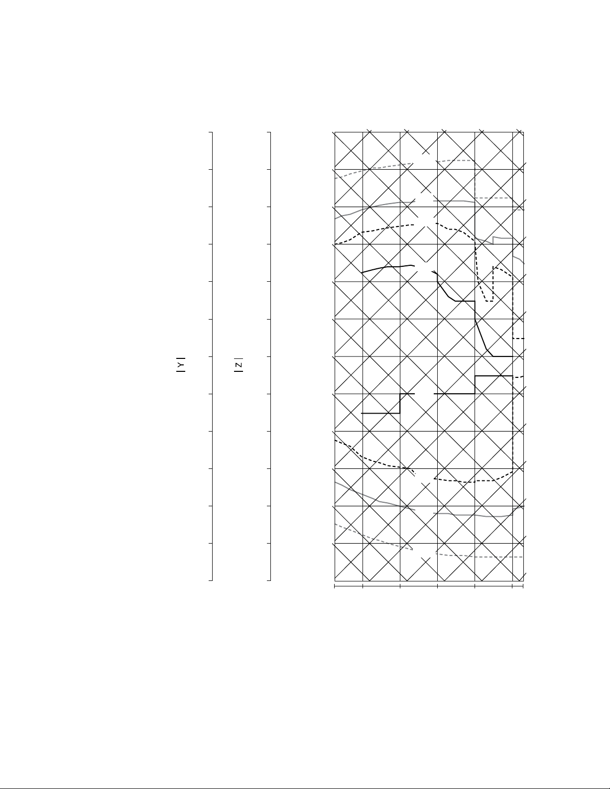
Measurement accuracy
The impedance measurement calculation example below is the result of absolute
measurement accuracy.
[ S ]
10n
100n
10μ
100μ
1m
10m
1kH
100aF
100H
10H
1H
10pF
1n
1G
100pF
100M
1nF
10M
1pF
100fF
1MH
100kH
10.0%
1.0%
10fF
10kH
1fF
0.3%
10nF
1μ
[Ω]
1M
100k
10k
100
100nF
1μF
10μF
1k
C
100μF
0.1%
0.1%
100mH
10mH
1mH
100μH
10μH
100m
100
1mF
10
10mF
1
1
0.3%
100mF
10
100m
10m
1.0%
1F
10.0%
10
1m
20 100 1k 10k 100k 1M 2M
Frequency [ Hz ]
Figure 1. Impedance measurement accuracy (Test signal voltage = 1 Vrms, cable length=0 m,
measurement time mode = MED)
1μH
100nH
10nH
1nH
100pH
16
Page 17

Compensation function
Table 28. The E4980A provides three types of compensation functions:
OPEN compensation, SHORT compensation, and LOAD compensation.
Type of compensation Description
OPEN compensation Compensates errors caused by the stray admittance (C, G)
of the test fixture.
SHORT compensation Compensates errors caused by the residual impedance (L, R)
of the test fixture.
LOAD compensation Compensates errors between the actual measured value
and a known standard value under the measurement conditions
desired by the user.
List sweep
Points: There is a maximum of 201 points.
Note
A parameter selected for one of the two
parameters cannot be selected for the other
parameter. It is not possible to set up a
combination of test signal voltage and test
signal current or one of test signal voltage of
DC bias signal and test signal current of DC bias.
The secondary parameter can be set only with
SCPI commands.
First sweep parameter (primary parameter): Test frequency, test signal voltage, test
signal current, test signal voltage of DC bias signal, test signal current of DC bias
signal, DC source voltage.
Second sweep parameter (secondary parameter): None, impedance range, test
frequency, test signal voltage, test signal current, test signal voltage of DC bias signal,
test signal current of DC bias signal, DC source voltage
Trigger mode
Sequential mode: When the E4980A is triggered once, the device is measured at all
sweep points. /EOM/INDEX is output only once.
Step mode: The sweep point is incremented each time the E4980A is triggered.
/EOM/INDEX is output at each point, but the result of the comparator function of the
list sweep is available only after the last /EOM is output.
17
Page 18

Comparator function of list sweep: The comparator function enables setting one pair of
lower and upper limits for each measurement point.
You can select from: Judge with the first sweep parameter/Judge with the second
parameter/Not used for each pair of limits.
Time stamp function: In the sequential mode, it is possible to record the measurement
starting time at each measurement point by defining the time when FW detects a trigger
as 0 and obtain it later with the SCPI command.
Comparator function
Bin sort: The primary parameter can be sorted into 9 BINs, OUT_OF_BINS, AUX_BIN,
and LOW_C_REJECT. The secondary parameter can be sorted into HIGH, IN, and LOW.
The sequential mode and tolerance mode can be selected as the sorting mode.
Limit setup: Absolute value, deviation value, and % deviation value can be used for setup.
BIN count: Countable from 0 to 999999.
DC bias signal
Table 29. Test signal voltage
Range 0 V to +2 V
Resolution 0 V / 1.5 V / 2 V only
Accuracy 0.1% + 2 mV (23 °C ± 5 °C)
(0.1% + 2 mV) × 4
(0 to 18 °C or 28 to 55 °C)
Note
The following USB memory can be used.
Complies with USB 1.1; mass storage class,
FAT16/FAT32 format; maximum consumption
current is below 500 mA.
Recommended USB memory: 4 GB USB Flash
memory (Agilent PN 1819-0637).
Use the recommended USB memory device
exclusively for the E4980A, otherwise,
previously saved data may be cleared. If you
use a USB memory other than the recommended device, data may not be saved or recalled
normally.
Agilent Technologies will NOT be responsible
for data loss in the USB memory caused by
using the E4980A.
Output impedance: 100 Ω (nominal)
Measurement assistance functions
Data buffer function: Up to 201 measurement results can be read out in a batch.
Save/Recall function:
• Up to 10 setup conditions can be written to/read from the built-in non-volatile memory.
• Up to 10 setup conditions can be written to/read from the USB memory.
• Auto recall function can be performed when the setting conditions are written to
Register 10 of the USB memory.
Key lock function: The front panel keys can be locked.
GPIB: 24-pin D-Sub (Type D-24), female; complies with IEEE488.1, 2 and SCPI.
USB host port: Universal serial bus jack, type-A (4 contact positions, contact 1 is on
your left), female (for connection to USB memory only).
USB interface port: Universal serial bus jack, type mini-B (4 contact positions); complies
with USBTMC-USB488 and USB 2.0; female; for connection to the external controller.
USBTMC: Abbreviation for USB Test & Measurement Class
LAN: 10/100 BaseT Ethernet, 8 pins (two speed options)
LXI Compliance: Class C (only applies to units with firmware revision A.02.00 or later)
18
Page 19

Options
Note
Option xxx is described as E4980A-xxx in the
order information
The following options are available for the E4980A LCR Meter.
Frequency options
None of below 20 Hz to 2 MHz
Option 030 20 Hz to 300 kHz
Option 050 20 Hz to 500 kHz
Option 100 20 Hz to 1 MHz
Table 30. Installable options
Options 2 MHz 300 kHz/500 kHz/1 MHz
Power and DC bias enhancement (001) installable not installable
Bias Current Interface (002) installable not installable
Entry model (005) installable not installable
Standard model (007) installable not installable
DCR measurement (200) installable
Handler interface (201) installable installable
Scanner interface (301) installable installable
1
not installable
2
Interface options
Option 002 (Bias current interface)
Adds a digital interface to allow the E4980A to control the 42841A’s bias current source.
Note
Option 007 can be installed only in the E4980A with
option 005.
Note
Option 200, 001, 030, 050, and 100 supports DCR
measurement function.
Option 201 (Handler interface)
Adds handler interface.
Option 301 (Scanner interface)
Adds scanner interface.
Option 710 (No interface)
An option with no interface.
Up to 2 interface options can be installed in the interface connector on the rear panel.
When no interface is installed, two of the option 710 are installed. When one interface
is installed, the option number of its interface and one option 710 are installed.
Other options
Option 001 (Power and DC Bias enhancement)
Increases test signal voltage and adds the variable DC bias voltage and DCR
measurement funciton.
Option 005 (Entry model)
Low-priced option that requires a longer measurement time. The level of measurement
accuracy is the same as the standard.
Option 007 (Standard model)
Upgrades the entry model to the standard.
Option 200 (DCR measurement)
Adds DCR measurement
1. Mandatory option
2. DCR measurement function is equipped by default.
19
Page 20

Power and DC Bias enhancement specification
Increases test signal voltage and adds the variable DC bias voltage function.
This function is available when the option 001 is installed.
Measurement parameters
The following parameters can be used.
• Lp-Rdc
• Ls-Rdc
• Vdc-Idc
where
Rdc Direct-current resistance (DCR)
Vdc Direct-current voltage
Idc Direct-current electricity
Test signal
Signal level
Table 31. Test signal voltage
Range 0 Vrms to 20 Vrms (test frequency ≤ 1 MHz)
0 Vrms to 15 Vrms (test frequency > 1 MHz)
Resolution 100 µVrms (0 Vrms - 0.2 Vrms)
200 µVrms (0.2 Vrms - 0.5 Vrms)
500 µVrms (0.5 Vrms - 1 Vrms)
1 mVrms (1 Vrms - 2 Vrms)
2 mVrms (2 Vrms - 5 Vrms)
5 mVrms (5 Vrms - 10 Vrms)
10 mVrms (10 Vrms - 20 Vrms)
Setup accuracy normal ±(10% + 1 mVrms) (test signal voltage ≤ 2 Vrms)
(test frequency ≤ 1 MHz : spec., test frequency > 1 MHz : typ.)
±(10% + 10 mVrms) (Test frequency ≤ 300 kHz,
test signal voltage > 2 Vrms) (spec.)
±(15% + 20 mVrms) (test frequency > 300 kHz,
test signal voltage > 2 Vrms) (test frequency ≤ 1 MHz : spec.,
test frequency > 1 MHz : typ.)
Constant1 ±(6% + 1 mVrms) (test signal voltage ≤ 2 Vrms)
(test frequency ≤ 1 MHz : spec. , test frequency > 1 MHz : typ.)
±(6% + 10 mVrms) (test frequency ≤ 300 kHz,
test signal voltage > 2 Vrms) (spec.)
±(12% + 20 mVrms) (test frequency > 300 kHz,
test signal voltage > 2 Vrms) (test frequency ≤ 1 MHz : spec.,
test frequency > 1 MHz : typ.)
1. When auto level control function is on.
20
Page 21

Table 32. Test signal current
Range 0 Arms - 100 mArms
Resolution 1 µArms (0 Arms - 2 mArms)
2 µArms (2 mArms - 5 mArms)
5 µArms (5 mArms - 10 mArms)
10 µArms (10 mArms - 20 mArms)
20 µArms (20 mArms - 50 mArms)
50 µArms (50 mArms - 100 mArms)
Setup accuracy normal ±(10% + 10 µArms) (test signal voltage ≤ 20 mArms)
(test frequency ≤ 1 MHz : spec., test frequency > 1 MHz : typ.)
±(10% + 100 µArms) (test frequency ≤ 300 kHz,
test signal current > 20 mArms) (spec.)
±(15% + 200 µArms) (test frequency > 300 kHz,
test signal voltage > 20 mArms) (test frequency ≤ 1 MHz : spec.,
test frequency > 1 MHz : typ.)
Constant
(test frequency ≤ 1 MHz : spec. , test frequency > 1 MHz : typ.)
±(6% + 100 µArms) (test frequency ≤ 300 kHz,
test signal voltage > 20 mArms) (spec.)
±(12% + 200 µArms) (test frequency > 300 kHz,
test signal voltage > 20 mArms) (test frequency ≤ 1 MHz : spec.,
test frequency > 1 MHz : typ.)
1
±(6% + 10 µArms) (test signal voltage ≤ 20 mArms)
Test signal level monitor function
• Test signal voltage and test signal current can be monitored.
• Level monitor accuracy:
Table 33. Test signal voltage monitor accuracy (Vac)
Test signal voltage2 Test frequency Specification
5 mVrms to 2 Vrms ≤ 1 MHz ±(3% of reading value + 0.5 mVrms)
> 1MHz ±(6% of reading value + 1 mVrms)
> 2 Vrms ≤ 300 kHz ±(3% of reading value + 5 mVrms)
> 300 kHz ±(6% of reading value + 10 mVrms)
Table 34. Test signal current monitor accuracy (Iac)
Test signal current2 Test frequency Specification
50 µArms to 20 mArms ≤ 1 MHz ±(3% of reading value + 5 µArms)
> 1MHz ±(6% of reading value + 10 µArms)
> 20 mArms ≤ 300 kHz ±(3% of reading value + 50 µArms)
> 300 kHz ±(6% of reading value + 100 µArms)
3
1. When auto level control function is on.
2. This is not an output value but a displayed test
signal level
3. Typ. when test frequency is > 1 MHz with test
signal voltage > 10 Vrms.
21
Page 22

DC bias signal
Table 35. Test signal voltage
Range –40 V to +40 V
Resolution Setup resolution: 100 µV, effective
resolution: 330 µV ±(0 V - 5 V)
1 mV ±(5 V - 10 V)
2 mV ±(10 V - 20 V)
5 mV ±(20 V - 40 V)
Accuracy test signal voltage ≤ 2 Vrms 0.1% + 2 mV (23
(0.1% + 2 mV) x 4
(0 to 18 °C or 28 to 55 °C)
test signal voltage > 2 Vrms 0.1 % + 4 mV (23 °C ± 5 °C)
(0.1% + 4 mV) x 4
(0 to 18 °C or 28 to 55 °C)
°C ± 5 °C)
Table 36. Test signal current
Range –100 mA - 100 mA
Resolution Setup resolution: 1 µA, effective
resolution: 3.3 µA ±(0 A - 50 mA)
10 µA ±(50 mA - 100 mA)
DC bias voltage level monitor Vdc
(0.5% of reading value + 60 mV) × Kt
When using Vdc-Idc measurement: (spec.)
When using level monitor: (typ.)
Kt Temperature coefficient
DC bias current level monitor Idc
(A [%] of the measurement value + B [A]) × Kt
When using Vdc-Idc measurement: (spec.)
When using level monitor: (typ.)
A [%] When the measurement time mode is SHORT: 2%
When the measurement time mode is MED or LONG: 1%
B [A] given below
Kt Temperature coefficient
When the measurement mode is SHORT, double the following value.
22
Page 23

Table 37. Test signal voltage ≤ 0.2 Vrms (measurement time mode = MED, LONG)
DC bias Impedance range [Ω]
current range < 100 100 300, 1 k 3 k, 10 k 30k, 100 k
20 µA 150 µA 30 µA 3 µA 300 nA 45 nA
200 µA 150 µA 30 µA 3 µA 300 nA 300 nA
2 mA 150 µA 30 µA 3 µA 3 µA 3 µA
20 mA 150 µA 30 µA 30 µA 30 µA 30 µA
100 mA 150 µA 150 µA 150 µA 150 µA 150 µA
Table 38. 0.2 Vrms < test signal voltage ≤ 2 Vrms
(measurement time mode = MED, LONG)
DC bias Impedance range [Ω]
current range < 100 100, 300 1k, 3 k 10k, 30 k 100 k
20 µA 150 µA 30 µA 3 µA 300 nA 45 nA
200 µA 150 µA 30 µA 3 µA 300 nA 300 nA
2 mA 150 µA 30 µA 3 µA 3 µA 3 µA
20 mA 150 µA 30 µA 30 µA 30 µA 30 µA
100 mA 150 µA 150 µA 150 µA 150 µA 150 µA
Table 39. Test signal voltage > 2 Vrms (measurement time mode = MED, LONG)
DC bias Impedance range [Ω]
current range ≤ 300 1 k, 3 k 10k, 30 k 100 k
20 µA 150 µA 30 µA 3 µA 300 nA
200 µA 150 µA 30 µA 3 µA 300 nA
2 mA 150 µA 30 µA 3 µA 3 µA
20 mA 150 µA 30 µA 30 µA 30 µA
100 mA 150 µA 150 µA 150 µA 150 µA
Table 40. Input impedance (nominal)
Input
impedance Conditions
0 Ω Other than conditions below.
20 Ω Test signal voltage ≤ 0.2 Vrms, Impedance range ≥ 3 k Ω,
DC bias current range ≤ 200 µA
Test signal voltage ≤ 2 Vrms, Impedance range ≥ 10 kΩ,
DC bias current range ≤ 200 µA
Test signal voltage > 2 Vrms, Impedance range = 100 kΩ,
DC bias current range ≤ 200 µA
DC source signal
Table 41. Test signal voltage
Range –10 V to 10 V
Resolution 1 mV
Accuracy 0.1% + 3 mV (23
(0.1% + 3 mV) x 4
(0 to 18 °C or 28 to 55 °C)
°C ± 5 °C)
Table 42. Test signal current
Range –45 mA to 45 mA (nominal)
Output impedance
100 Ω (nominal)
23
Page 24

DCR measurement specification
DC resistance (Rdc) measurement function is available when either option 001, 030, 050,
100, or 200 is installed.
DC resistance (Rdc) accuracy
Absolute measurement accuracy Aa
Absolute measurement accuracy Aa is given as
Equation 15. Aa = Ae + Acal
Aa Absolute accuracy (% of reading value)
Ae Relative accuracy (% of reading value)
Acal Calibration accuracy
Relative measurement accuracy Ae
Relative measurement accuracy Ae is given as
Equation 16. Ae = [Ab + (Rs /|Rm|+ Go × |Rm|) × 100 ] × Kt
Rm Measurement value
Ab Basic accuracy
Rs Short offset [Ω]
Go Open offset [S]
Kt Temperature coefficient
Calibration accuracy Acal
Calibration accuracy Acal is 0.03%.
Basic accuracy Ab
Table 43. Basic accuracy Ab is given below.
Measurement Test signal voltage
time mode ≤ 2 Vrms > 2 Vrms
SHORT 1.00% 2.00%
MED 0.30% 0.60%
Open offset Go
Table 44. Open offset Go is given below.
Measurement Test signal voltage
time mode ≤ 2 Vrms > 2 Vrms
SHORT 50 nS 500 nS
MED 10 nS 100 nS
Short offset Rs
Table 45. Short offset Rs is given below.
Measurement Test signal voltage
time mode ≤ 2 Vrms > 2 Vrms
SHORT 25 mΩ 250 mΩ
MED 5 mΩ 50 mΩ
24
Page 25

Effect of cable length (Short offset)
Table 46. The following value is added to Rs when the cable is extended.
Cable length
1 m 2 m 4 m
0.25 mΩ 0.5 mΩ 1 mΩ
Temperature coefficient Kt
Table 47. Temperature coefficient Kt is given below.
Temperature [°C] Kt
0 - 18 4
18 - 28 1
28 - 55 4
25
Page 26
General specifications
Table 48. Power source
Voltage 90 VAC - 264 VAC
Frequency 47 Hz - 63 Hz
Power consumption Max. 150 VA
Table 49. Operating environment
Temperature 0 - 55 °C
Humidity 15% - 85% RH
(≤ 40 °C, no condensation)
Altitude 0 m - 2000 m
Table 50. Storage environment
Temperature –20 - 70 °C
Humidity 0% - 90% RH
( ≤ 60 °C, no condensation)
Altitude 0 m - 4572 m
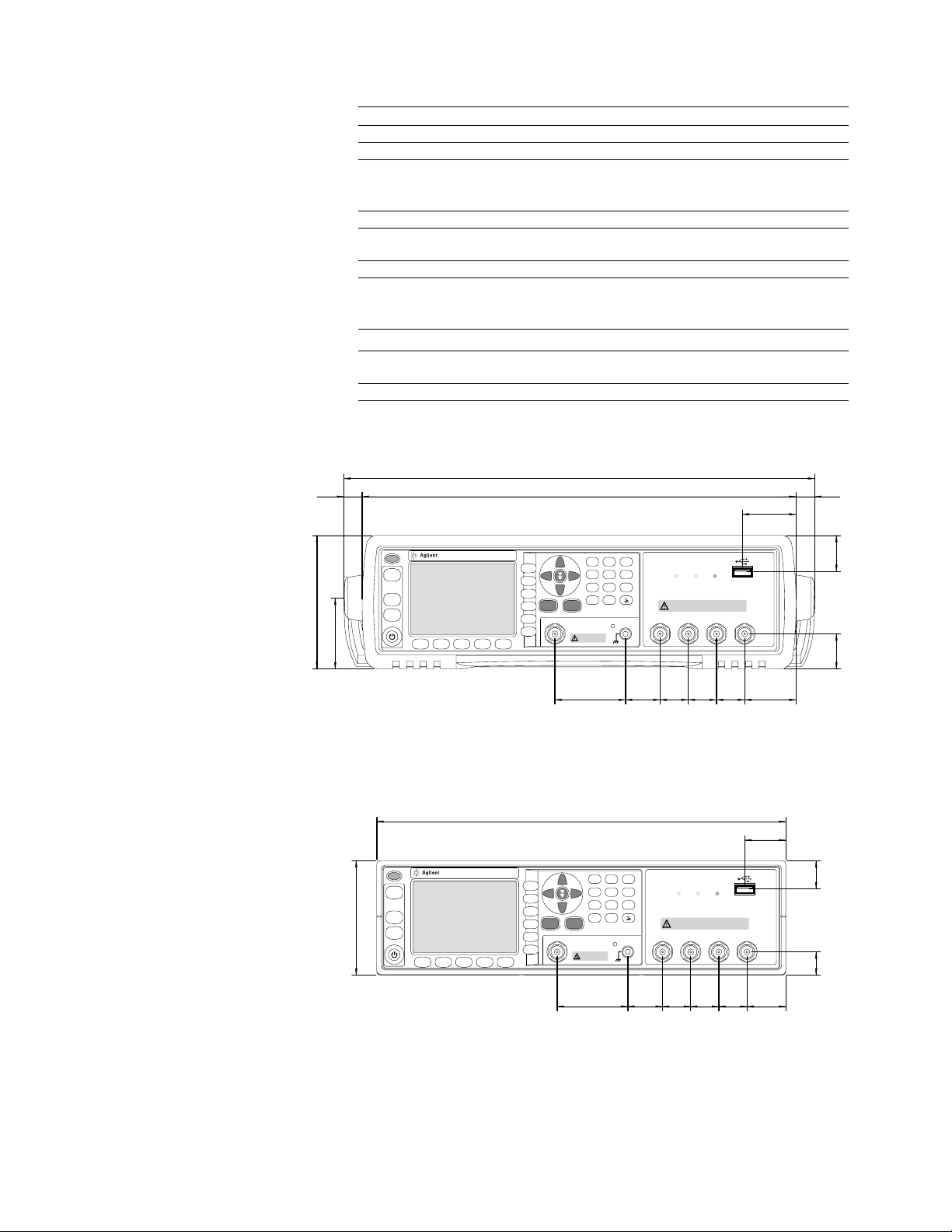
Outer dimensions: 375 (width) x 105 (height) × 390 (depth) mm (nominal)
367.4
14.4
338.6
14.4
41.8
20 Hz - 2 MHz
Recall A Recall B
E4980A
Precision LCR Meter
789
456
123
.
Meas
Setup
DC Source
(Option 001)
0
10VDC Max
Display
Format
Save/
Recall
Return
Local/
System
Lock
55.2
27
DC
Source
Discharge test device before connecting
42V Peak Max Output CAT I
L
CURLPOT
22
103.8
55.0
Preset
Trigger
DC Bias
DC
Source
Figure 2. Dimensions (front view, with handle and bumper, in millimeters, nominal)
319.1
E4980A
20 Hz - 2 MHz
Recall A Recall B
Precision LCR Meter
Save/
Recall
789
456
123
.
Meas
Setup
DC Source
(Option 001)
0
10VDC Max
Display
Format
Return
Local/
System
Lock
DC
Source
Discharge test device before connecting
42V Peak Max Output CAT I
L
CURLPOT
2755.2
88.3
Preset
Trigger
DC Bias
DC
Source
DC
Bias
UNKNOWN
22
DC
Bias
UNKNOWN
USB
H
POT
22
USB
H
POT
222222 30.3
28.0
H
CUR
27.3
40.1
32.0
21.8
H
CUR
18.0
26
Figure 3. Dimensions (front view, without handle and bumper, in millimeters, nominal)
Page 27
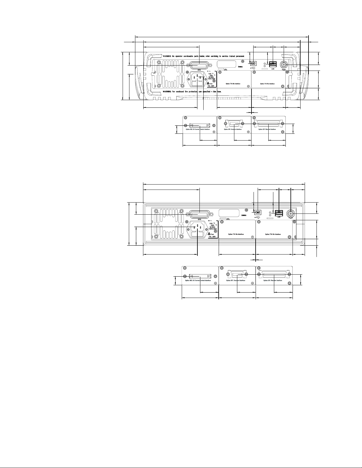
17.6
118.1
367.4
332.2
23.241.6 34.7
17.6
23.9
E4980A
Option 710: No Interface
101.6
115V
-230V
50/60Hz
150VA MAX
T3A , 250V
Serial Label
Option 710: No Interface
Fuse
GPIB
55.0 28.0
113.9 72.3 72.3 31.1
17.1
72.3
49.3
36.2
0.4
Option 301: Scanner Interface Option 201: Handler InterfaceOption 002: DC Current Control Interface
36.2
72.3
Figure 4. Dimensions (rear view, with handle and bumper, in millimeters, nominal)
317.8
110.9
19.6
Serial Label
E4980A
Option 710: No Interface
84.4
36.5 23.7
GPIB
115V
-230V
50/60Hz
150VA MAX
Fuse
T3A , 250V
25.7
LAN
36.2
72.3
21.3
Option 710: No Interface
Trigger
23.241.6 27.5
LAN
Trigger
26.63725.5
20.9
22.23712.7
106.7
72.3 72.3 24.0
0.4
Option 301: Scanner Interface Option 201: Handler InterfaceOption 002: DC Current Control Interface
Figure 5. Dimensions (front view, without handle and bumper, in millimeters, nominal)
27
Page 28

66.6
388.7
103.8
55.0
141.4
Figure 6. Dimensions (side view, with handle and bumper, in millimeters, nominal)
374.0
15.7
21.921.9
88.3
45.7
19.7
50.9
101.6
10.5347.9
84.4
Note
Effective pixels are more than 99.99%. There
may be 0.01% (approx. 7 pixels) or smaller
missing pixels or constantly lit pixels, but this
is not a malfunction.
Figure 7. Dimensions (side view, without handle and bumper, in millimeters, nominal)
Weight: 5.3 kg (nominal)
Display: LCD, 320 × 240 (pixels), RGB color
The following items can be displayed:
• measurement value
• measurement conditions
• limit value and judgment result of comparator
• list sweep table
• self-test message
28
Page 29
Description Supplemental Information
EMC
European Council Directive 2004/108/EC
IEC 61326-1:2005
EN 61326-1:2006
CISPR 11:2003 +A1:2004
EN 55011:1998 +A1:1999 +A2:2002 Group 1, Class A
IEC 61000-4-2:1995 +A1:1998 +A2:2000
EN 61000-4-2:1995 +A1:1998 +A2:2001 4 kV CD/8 kV AD
IEC 61000-4-3:2002
EN 61000-4-3:2002 3 V/m, 80-1000 MHz, 80% AM
IEC 61000-4-4:2004
EN 61000-4-4:2004 1 kV power /0.5 kV Signal
IEC 61000-4-5:1995 +A1:2000
EN 61000-4-5:1995 +A1:2001 0.5 kV Normal/1 kV Common
IEC 61000-4-6:1996 +A1:2000
EN 61000-4-6:1996 +A1:2001 3 V, 0.15-80 MHz, 80% AM
IEC 61000-4-11:2004
EN 61000-4-11:2004 100% 1 cycle
ICES/NMB-001
Cet appareil ISM est conforme a la norme NMB-001 du Canada.
AS/NZS CISPR11:2004 Group 1, Class A
This ISM device complies with Canadian ICES-001:2006.
Safety
European Council Directive 2006/95/EC
IEC 61010-1:2001/EN 61010-1:2001
Measurement Category I, Pollution Degree 2, Indoor Use
IEC60825-1:1994 Class 1 LED
CAN/CSA C22.2 61010-1-04
Measurement Category I, Pollution Degree 2, Indoor Use
Environment
This product complies with the WEEE Directive (2002/96/EC)
marking requirements. The affixed label indicates that you must
not discard this electrical/electronic product in domestic house
hold waste.
Product Category: With reference to the equipment types in the
WEEE Directive Annex I, this product is classed as a “Monitoring
and Control instrumentation” product.
29
Page 30
Supplemental
Information
Note
Discharge capacitors before connecting them
to the UNKNOWN terminal or a test fixture to
avoid damages to the instrument.
Settling time
Table 51. Test frequency setting time
Test frequency setting time Test frequency (Fm)
5 ms Fm ≥ 1 kHz
12 ms 1 kHz > Fm ≥ 250 Hz
22 ms 250 Hz > Fm ≥ 60 Hz
42 ms 60 Hz > Fm
Table 52. Test signal voltage setting time
Test signal voltage setting time Test frequency (Fm)
11 ms Fm ≥ 1 kHz
18 ms 1 kHz > Fm ≥ 250 Hz
26 ms 250 Hz > Fm ≥ 60 Hz
48 ms 60 Hz > Fm
Switching of the impedance range is as follows:
≤ 5 ms/ range switching
Measurement circuit protection
The maximum discharge withstand voltage, where the internal circuit remains protected
if a charged capacitor is connected to the UNKNOWN terminal, is given below.
Table 53. Maximum discharge withstand voltage
Maximum discharge withstand voltage Range of capacitance value C of DUT
1000 V C < 2 µF
√
2 µF ≤ C
2/C V
30
1200
1000
800
600
400
Voltage [V]
200
0
1.E–15 1.E–13 1.E–11 1.E–09 1.E–07 1.E–05 1.E–03
Capacitance [F]
Figure 8. Maximum discharge withstand voltage
Page 31
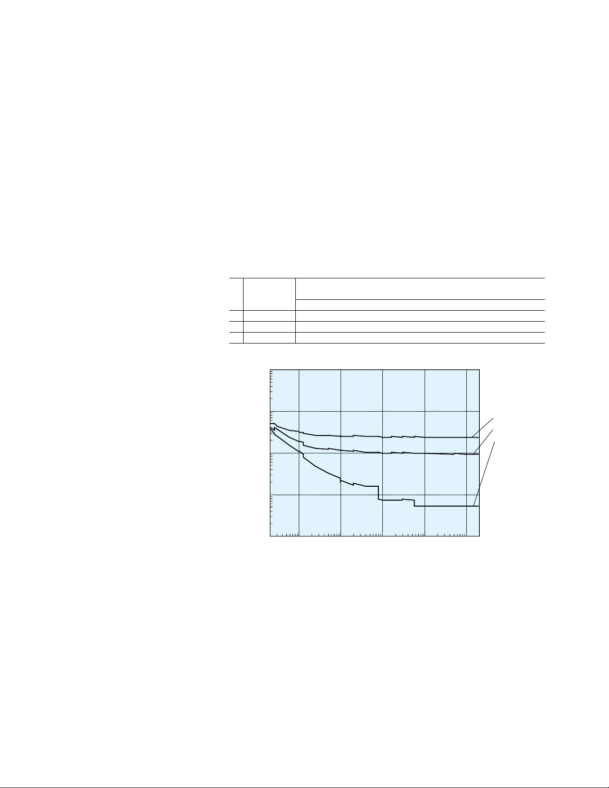
Measurement time
10
Definition
This is the time between the trigger and the end of measurement (EOM) output on the
handler interface.
Conditions
Table 54 shows the measurement time when the following conditions are satisfied:
• Normal impedance measurement other than Ls-Rdc, Lp-Rdc, Vdc-Idc
• Impedance range mode: hold range mode
• DC bias voltage level monitor: OFF
• DC bias current level monitor: OFF
• Trigger delay: 0 s
• Step delay: 0 s
• Calibration data: OFF
• Display mode: blank
Table 54. Measurement time [ms](DC bias:OFF)
Measurement
time mode Test frequency
1 LONG 480 300 240 230 220 220 220
2 MED 380 180 110 92 89 88 88
3 SHORT 330 100 20 7.7 5.7 5.6 5.6
20 Hz 100 Hz 1 kHz 10 kHz 100 kHz 1 MHz 2 MHz
1
0.1
Measurement time [sec]
0.01
0.001
20 100 1k 10k 100k 1M 2M
Test frequency [Hz]
Figure 9. Measurement time (DC bias: OFF)
1. LONG
2. MED
3. SHORT
31
Page 32

Table 55. Measurement time when option 030/050/100 is installed [ms]
M
i
[
]
Measurement
time mode Test frequency
1 LONG 729 423 363 353 343 343
2 MED 650 250 140 122 119 118
3 SHORT 579 149 26 14 12 12
10
20 Hz 100 Hz 1 kHz 10 kHz 100 kHz 1 MHz
1
sec
me
0.1
easurement t
0.01
0.001
20 100 1k 10k 100k 1M 2M
Test frequency [Hz]
Figure 10. Measurement time (Option 030/050/100)
1. LONG
2. MED
3. SHORT
Table 56. Measurement time when option 005 is installed [ms]
(DC bias: OFF)
Measurement
time mode Test frequency
1 LONG 1190 650 590 580 570 570 570
2 MED 1150 380 200 180 180 180 180
3 SHORT 1040 240 37 25 23 23 23
20 Hz 100 Hz 1 kHz 10 kHz 100 kHz 1 MHz 2 MHz
10
1
0.1
Measurement time [sec]
0.01
0.001
20 100 1k 10k 100k 1M 2M
Test frequency [Hz]
Figure 11. Measurement time (DC bias: OFF, Option 005)
1. LONG
2. MED
3. SHORT
32
Page 33

When DC bias is ON, the following time is added:
Table 57. Additional time when DC bias is ON [ms]
Test frequency
20 Hz 100 Hz 1 kHz 10 kHz 100 kHz 1 MHz 2 MHz
30 30 10 13 2 0.5 0.5
When the number of averaging increases, the measurement time is given as
Equation 17. MeasTime + (Ave – 1) × AveTime
MeasTime Measurement time calculated based on Table 53 and Table 54
Ave Number of averaging
AveTime Refer to Table 56
Table 58. Additional time per averaging [ms]
Measurement
time mode Test frequency
20 Hz 100 Hz 1 kHz 10 kHz 100 kHz 1 MHz 2 MHz
SHORT 51 11 2.4 2.3 2.3 2.2 2.2
MED 110 81 88 87 85 84 84
LONG 210 210 220 220 220 210 210
Table 59. Measurement time when Vdc-Idc is selected [ms]
Measurement time mode 20 Hz 100 Hz 1 kHz 10 kHz 100 kHz 1 MHz 2 MHz
SHORT 210 46 14 14 14 14 14
MED 210 170 170 170 170 170 170
LONG 410 410 410 410 410 410 410
Test frequency
Add the same measurement time per 1 additional average
Additional Measurement time when the Vdc and Idc monitor function is ON.
Add SHORT mode of Table 59. When using only Vdc or Idc, add a half of SHORT mode of
Table 59.
Table 60. Measurement time when Ls-Rdc or Lp-Rdc is selected [ms]
Test frequency
Measurement time mode 20 Hz 100 Hz 1 kHz 10 kHz 100 kHz 1 MHz 2 MHz
SHORT 910 230 43 24 22 22 22
MED 1100 450 300 280 270 270 270
LONG 1400 820 700 670 660 650 650
Add the three times of measurement time per 1 additional average number
33
Page 34

Display time
Except for the case of the DISPLAY BLANK page, the time required to update the display
on each page (display time) is as follows. When a screen is changed, drawing time and
switching time are added. The measurement display is updated about every 100 ms.
Table 61. Display time
When Vdc, Idc When Vdc, Idc
Item monitor is OFF monitor is ON
MEAS DISPLAY page drawing time 10 ms 13 ms
MEAS DISPLAY page (large) drawing time 10 ms 13 ms
BIN No. DISPLAY page drawing time 10 ms 13 ms
BIN COUNT DISPLAY page drawing time 10 ms 13 ms
LIST SWEEP DISPLAY page drawing time 40 ms —
Measurement display switching time 35 ms —
Measurement data transfer time
This table shows the measurement data transfer time under the following conditions.
The measurement data transfer time varies depending on measurement conditions and
computers.
Table 62. Measurement transfer time under the following conditions:
Host computer: DELL OPTIPLEX GX260 Pentium 4 2.6 GHz
Display: ON
Impedance range mode: AUTO (The overload has not been generated.)
OPEN/SHORT/LOAD compensation: OFF
Test signal voltage monitor: OFF
Table 63. Measurement data transfer time [ms]
using :FETC? command using data buffer memory
Data (one point measurement) (list sweep measurement)
transfer Comparator Comparator 10 51 128 201
Interface format ON OFF points points points points
ASCII 2 2 4 13 28 43
GPIB ASCII Long 2 2 5 15 34 53
Binary 2 2 4 10 21 32
ASCII 2 2 3 8 16 23
USB ASCII Long 2 2 4 9 19 28
Binary 2 2 3 5 9 13
ASCII 3 4 5 12 24 36
LAN ASCII Long 3 3 5 13 29 44
Binary 3 3 5 9 18 26
34
Page 35

DC bias test signal current (1.5 V/2.0 V): Output current: Max. 20 mA
Option 001 (Power and DC Bias enhance):
DC bias voltage: DC bias voltage applied to DUT is given as:
Equation 18. Vdut = Vb – 100 × Ib
Vdut [V] DC bias voltage
Vb [V] DC bias setting voltage
Ib [A] DC bias current
DC bias current: DC bias current applied to DUT is given as:
Equation 19. Idut = Vb/(100 + Rdc)
Idut [A] DC bias current
Vb [V] DC bias setting current
Rdc [Ω] DUT’s DC resistance
Maximum DC bias current
Table 64. Maximum DC bias current when the normal measurement
can be performed.
Bias current isolation
Impedance OFF
range [Ω]
0.1 20 mA 100 mA
1 20 mA 100 mA
10 20 mA 100 mA
100 20 mA 100 mA
300 2 mA 100 mA
1 k 2 mA 20 mA
3 k 200 µA 20 mA
10 k 200 µA 2 mA
30 k 20 µA 2 mA
100 k 20 µA 200 µA
ON
Auto range
mode: 100 mA
Hold range mode:
its values for
the range.
Test signal voltage ≤ 2 Vrms Test signal voltage > 2 Vrms
When DC bias is applied to DUT
When DC bias is applied to the DUT, add the following value to the absolute accuracy Ab.
Table 65. Only when Fm < 10 kHz and |Vdc| > 5 V
SHORT MED, LONG
0.05% × (100 mV/Vs) × (1 + √(100/Fm)) 0.01% × (100 mV/Vs) × (1 + √(100/Fm))
Fm [Hz] Test frequency
Vs [V] Test signal voltage
Relative measurement accuracy with bias current isolation
When DC bias Isolation is set to ON, add the following value to the open offset Yo.
Equation 20. Yo_DCI1 × (1 + 1/(Vs)) × (1 + √(500/Fm)) + Yo_DCI2
Zm [Ω] Impedance of DUT
Fm [Hz] Test frequency
Vs [V] Test signal voltage
Yo_DCI1,2 [S] Calculate this by using Table 61 and 62
Idc [A] DC bias isolation current
35
Page 36

Table 66. Yo_DCI1 value
DC bias current range Measurement time mode
SHORT MED, LONG
20 µA 0 S 0 S
200 µA 0.25 nS 0.05 nS
2 mA 2.5 nS 0.5 nS
20 mA 25 nS 5 nS
100 mA 250 nS 50 nS
Table 67. Yo_DCI2 value
DC bias Measurement time mode
current range ≤ 100 Ω 300 Ω, 1 k Ω 3 k Ω, 10 k Ω 30 k Ω, 100 k Ω
20 µA 0 S 0 S 0 S 0 S
200 µA 0 S 0 S 0 S 0 S
2 mA 0 S 0 S 0 S 3 nS
20 mA 0 S 0 S 30 nS 30 nS
100 mA 0 S 300 nS 300 nS 300 nS
DC bias settling time
When DC bias is set to ON, add the following value to the settling time:
Table 68. DC bias settling time
Bias Settling time
1 Standard Capacitance of DUT × 100 × loge (2/1.8 m) + 3 m
2 Option 001 Capacitance of DUT × 100 × loge (40/1.8 m) + 3 m
100 sec
10 sec
1 sec
100 msec
Settling time
10 msec
Figure 12. DC bias settling time
2.
1.
1 µF 10 µF 100 µF 1 mF 10 mF 100 mF
DUT capacitance
36
Page 37

www.agilent.com
Web Resources
Visit our Web sites for additional
product information
and literature.
E4980A Precision LCR Meter
www.agilent.com/find/e4980a
E4980AL Precision LCR Meter
www.agilent.com/find/e4980al
LCR Meters & Impedance
Measurement Products
www.agilent.com/find/impedance
RF & MW test accessories
www.agilent.com/find/mta
myAgilent
www.agilent.com/find/myagilent
A personalized view into the information
most relevant to you.
www.lxistandard.org
LAN eXtensions for Instruments puts
the power of Ethernet and the Web
inside your test systems. Agilent is a
founding member of the LXI consortium.
Three-Year Warranty
www.agilent.com/find/ThreeYearWarranty
Agilent’s combination of product reliability
and three-year warranty coverage is another
way we help you achieve your business goals:
increased confidence in uptime, reduced cost
of ownership and greater convenience.
Agilent Advantage Services
www.agilent.com/find/AdvantageServices
Accurate measurements throughout the
life of your instruments.
www.agilent.com/quality
For more information on Agilent
Technologies’ products, applications or
services, please contact your local Agilent
office. The complete list is available at:
www.agilent.com/find/contactus
Americas
Canada (877) 894 4414
Brazil (11) 4197 3600
Mexico 01800 5064 800
United States (800) 829 4444
Asia Pacifi c
Australia 1 800 629 485
China 800 810 0189
Hong Kong 800 938 693
India 1 800 112 929
Japan 0120 (421) 345
Korea 080 769 0800
Malaysia 1 800 888 848
Singapore 1 800 375 8100
Taiwan 0800 047 866
Other AP Countries (65) 375 8100
Europe & Middle East
Belgium 32 (0) 2 404 93 40
Denmark 45 45 80 12 15
Finland 358 (0) 10 855 2100
France 0825 010 700*
*0.125 €/minute
Germany
49 (0) 7031 464 6333
Ireland 1890 924 204
Israel 972-3-9288-504/544
Italy 39 02 92 60 8484
Netherlands 31 (0) 20 547 2111
Spain 34 (91) 631 3300
Sweden 0200-88 22 55
United Kingdom 44 (0) 118 927 6201
For other unlisted countries:
www.agilent.com/find/contactus
(BP-3-1-13)
Agilent Channel Partners
www.agilent.com/find/channelpartners
Get the best of both worlds: Agilent’s
measurement expertise and product
breadth, combined with channel
partner convenience.
Product specifications and descriptions
in this document subject to change
without notice.
© Agilent Technologies, Inc. 2013
Published in USA, May 11, 2013
5989-4435EN
 Loading...