

Page 1
Which
Product
Meets
Your
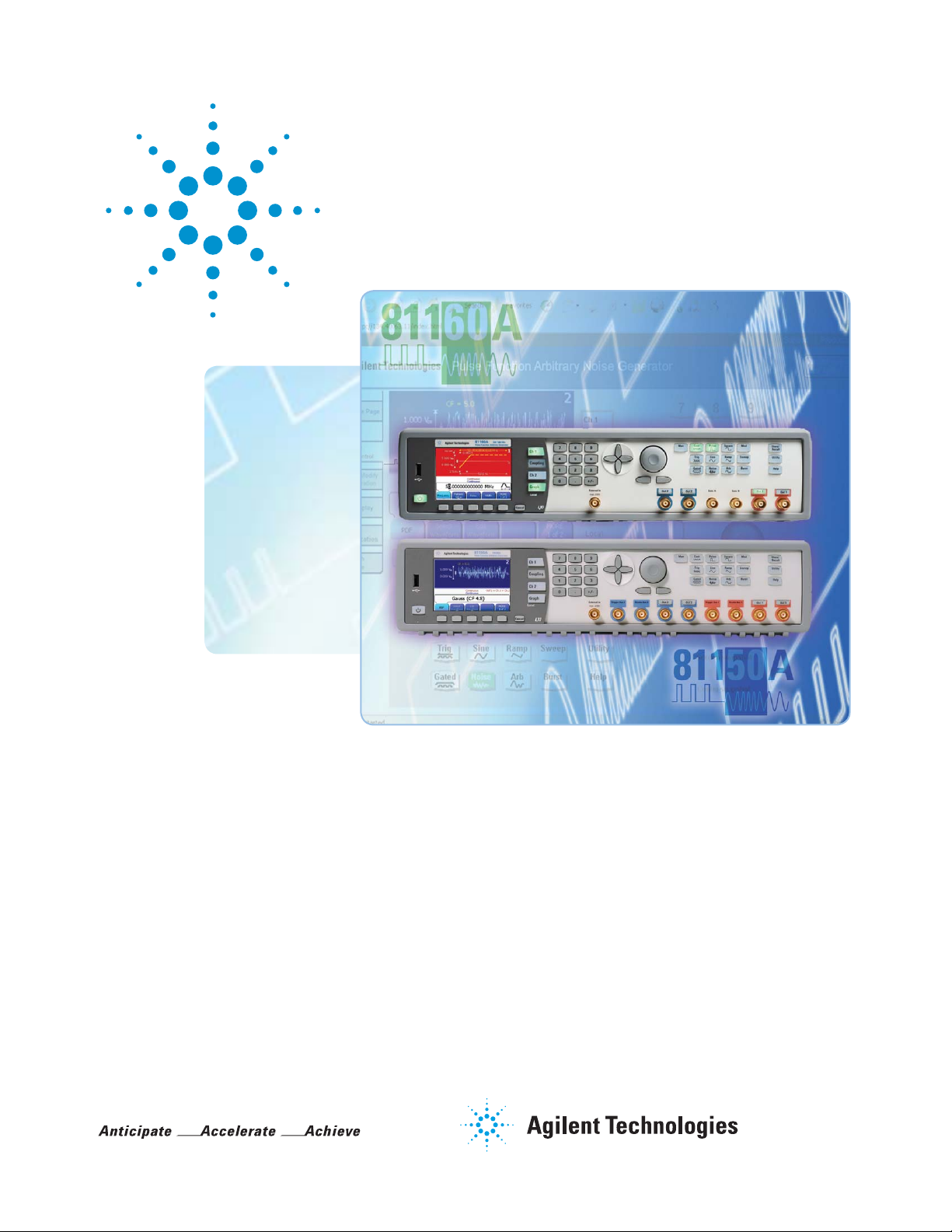
Agilent 81150A and 81160A
Pulse Function Arbitrary Noise Generators
Data Sheet, Version 1.1
Needs?
High precision pulse generators enhanced with versatile signal
generation, modulation and distortion capabilities for:
• Accurate signals to test your device and not your signal source
• Versatile waveform and noise generation to be ready for today‘s
and tomorrow‘s stress test challenges
• Optional pattern generator to test in addition to analog, digital
and mixed signal devices
• Integrated into one instrument to minimize cabling, space and
test time
Page 2

The 81150A Pulse Function
Arbitrary Noise Generator
at a Glance
811
50
A
• 1 µHz – 120 MHz pulse generation with variable rise/fall time
• 1 µHz – 240 MHz sine waveform output
• 14-bit, 2 GSa/s arbitrary waveforms
• 512k samples deep arbitrary waveform memory per channel
• Pulse, sine, square, ramp, noise and arbitrary waveforms
• Noise, with selectable crest factor, and signal repetition time of 26 days
• FM, AM, PM, PWM, FSK modulation capabilities
• 1 or 2 channel, coupled and uncoupled
• Differential outputs
• Two selectable output amplifi ers:
◦ High bandwidth amplifier
Amplitude: 50 mV
100 mVpp to 10 V
Voltage window: ± 5 V; 50 Ω into 50 Ω
± 10 V; 50 Ω into open
± 9 V; 5 Ω into 50 Ω
◦ High voltage amplifier
Amplitude: 100 mV
200 mV
to 20 VPP; 5 Ω into 50 Ω, or 50 Ω into open
PP
to 5 VPP; 50 Ω into 50 Ω
PP
; 50 Ω into open
PP
to 10 VPP; 50 Ω into 50 Ω,
PP
Voltage window: ± 10 V; 50 Ω into 50 Ω
± 20 V; 5 Ω into 50 Ω or 50 Ω into open
• Glitch free change of timing parameters
(delay, frequency, transition time, width, duty cycle)
• Programming language compatible with Agilent 81101A, 81104A, 81105A,
81110A, 81130A and 81160A
• ISO 17025 and Z540.3 calibration
• LXI class C (rev. 1.1) compliant
• Optional pattern generator:
◦ Ideal and arbitrary bit shaped pattern up to 120 Mbit/s
◦ Two, three or four level signals
◦ PRBS up to 2
◦ 16 Mbit pattern memory
◦ Pass through pattern for combined and physical and protocol test up to 10 Mbit/s
31
2
Page 3

The 81160A Pulse Function
Arbitrary Noise Generator
at a Glance
811
60
A
• 1 µHz – 330 MHz pulse generation with variable rise/fall time
• 1 µHz – 500 MHz sine waveform output
• 14-bit, 2.5 GSa/s arbitrary waveforms
• Up to 256k samples deep arbitrary waveform memory per channel
• Pulse, sine, square, ramp, noise and arbitrary waveforms
• Noise, with selectable crest factor, and signal repetition time of 20 days
• FM, AM, PM, PWM, FSK modulation capabilities
• 1 or 2 channel, coupled and uncoupled
• Differential outputs
◦ Amplitude:
50 Ω into 50 Ω 50 mV
50 Ω into open 100 mVPP to 10 V
◦ Voltage window:
50 Ω into 50 Ω ± 5 V
50 Ω into open ± 10 V
• Glitch free change of timing parameters
(delay, frequency, transition time, width, duty cycle)
• Programming language compatible with Agilent 81101A, 81104A, 81105A , 81110A,
81130A and 81150A
• ISO 17025 and Z540.3 calibration
• LXI class C (rev 1.1) compliant
• Optional pattern generator:
◦ Ideal and arbitrary bit shaped pattern up to 330 Mbit/s (Option 330) or 660 Mbit/s
(Option 660)
◦ Two, three or four level signals
◦ PRBS up to 2
◦ 4 Mbit pattern memory for the 1-channel instrument and 2 Mbit per channel for the
2-channel instrument
◦ Pass through pattern for combined and physical and protocol test up to 10 Mbit/s
31
to 5 V
PP
PP
PP
3
Page 4
811
50
A
Waveform type
USB 2.0A
Couple/uncouple channels
External In
Trigger mode
Channel 2:
Trigger Out
Strobe Out
Differential output
Advanced mode
Channel 1:
Trigger Out
Strobe Out
Differential output
USB 2.0A
USB 2.0 B
LAN
10 MHz Ref In
Modulation In 1, 2
10 MHz Ref Out
GPIB
4
Page 5
811
60
A
Waveform type
USB 2.0A
Couple/uncouple channels
External In
Channel 2:
Differential output
Trigger mode
Sync out A and B:
The logical trigger signal 1
or logical trigger signal 2
or logical strobe signal 1
or logical strobe signal 2
can be routed by a fully
fl exible internal switch
matrix to Sync Out A or
Sync Out B.
Advanced mode
Channel 1:
Differential
output
10 MHz Ref Out
10 MHz Ref In
Modulation
In 1, 2
USB 2.0A
GPIB
USB 2.0B
LAN
5
Page 6
Today‘s Challenges Require
a New Generation of Test
Instruments
You are under pressure to get products to market faster and faster, with shrinking design
schedules and increasing quality goals. The pressure is never ending. Because differentiation means survival in the marketplace, you often have to test unique functionality. Being
confi dent in your results takes highly adaptable and effi cient testing.
Such challenges require a new generation of test instruments, which are:
• Accurate, to test your device and not your source
• Versatile, to be ready for today’s and tomorrows test challenges
• Plug and play solutions, with minimal cabling, low space overhead and
have many functions built-in
Whichever way you look at it, this starts with accurate, versatile and uncompromising
signal sources.
Just test – with the signal you need.
Quad versatility – optimum signal fi delity
Agilent’s offering
The Agilent 81150A and 81160A Pulse Function Arbitrary Noise Generators set the
standard for the next generation of lab: for fast, accurate insight into your design or device
under test. Both of them offer:
• Pulse generators with precise signals for performance verification and characterization
• A function arbitrary generator
◦ For versatile signal generation to optimize testing
◦ For modulation to shape the signal the DUT needs
• A noise generator to distort signals to build up worst case scenarios
• An optional pattern generator to test in addition to analog, digital and mixed signal
devices with ideal and real-world conditions
The Agilent 81150A and the new Agilent 81160A Pulse Function Arbitrary Noise
Generators are indispensable contributors to accelerate ideal and real-world testing.
Pulse
generator
Pattern
generator
Function arbitrary
generator
Figure 1. Agilent 81150A and 81160A Pulse Function Arbitrary Noise Generator
6
Noise
generator
Page 7
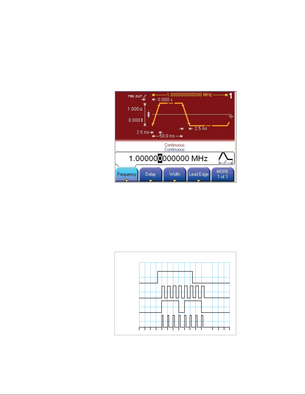
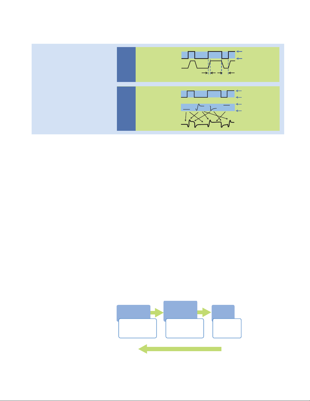
Pulse Generator – Test
Your Device and Not Your
Source
Channel 1 pulse setup
Superior precision pulses with unbeatable timing stability guarantee reproducible tests.
The signal quality and trigger functionality provide everything you need for trigger or
system clock applications.
You can change the timing parameters (delay, frequency, transition time, width, duty
cycle) without dropouts or glitches. This patented, industry-leading feature means
continuous operation without having to reboot or reset your device under test, for
example when you are characterizing a device by sweeping the clock frequency. Apart
from full control of the timing parameters, you can also adjust levels and edges as needed.
Set up complex measurements
Measurement using strobe and trigger
Both, the Agilent 81150A and the Agilent 81160A Pulse Function Arbitrary Noise Generator, are available in a 1 or 2 channel version. On the two channel version, the channels
can be uncoupled, to work independently, or coupled, for example, with a defi ned delay
between them.
Each channel provides Trigger Out, Strobe Out and differential outputs: the basis for many
complex test setups.
Gated Burst of 4
External In
Trigger Out
Strobe Out
Out
7
Page 8
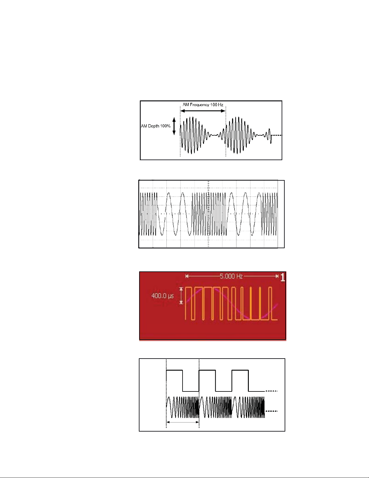
Function Arbitrary Generator
– Stress Your Device to its Limit
Amplitude modulation
Frequency shift keying modulation
If you need further signal conditioning, the Agilent 81150A and the Agilent 81160A Pulse
Function Arbitrary Noise Generators provide versatile waveforms and modulation capabilities to adapt your signal to your device’s requirements. AM, FM, FSK, PM and PWM are
available at modulation frequencies up to 10 MHz and to 50 MHz.
The Agilent 81150A and the Agilent 81160A Pulse Function Arbitrary Noise Generators
can use internal or external modulation sources. Internal modulation can be generated
from the 2nd channel or the internal modulation source of the modulated channel.
Pulse width modulation
Frequency sweep
Strobe Out
Out 1
Sweep Time
8
Page 9
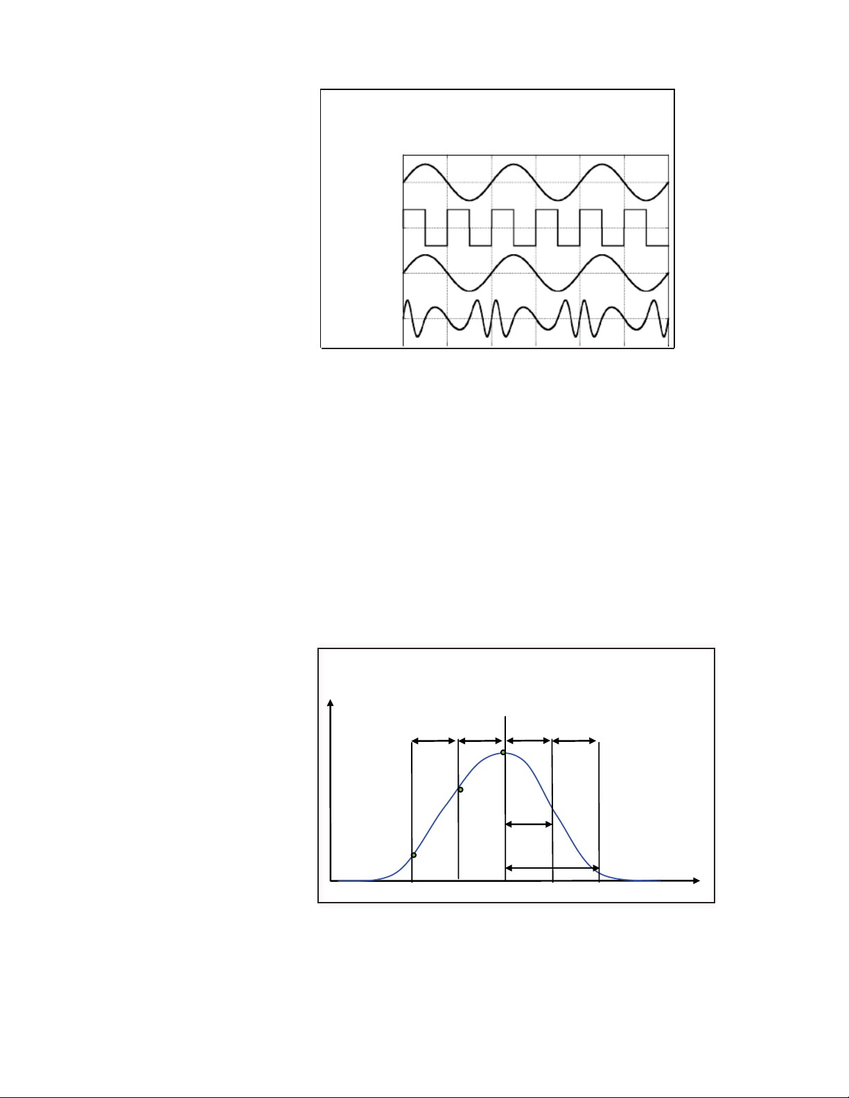
Setting up a measurement using
trigger, strobe, modulation and carrier
Contin uous PM
Phase Deviat ion 180 deg.
Carr i er Sin ew ave 0.04 MHz
Modulat ed by Si newave 0.02 MHz
Modulat ion
Si gn a l
T r i gger Out
St r obe Out
Out
Noise generator – repeatable and
stochastic noise
Gaussian curve and distribution
Jitter and noise cause misalignment of edges and levels, resulting in data errors. Noise is
by its nature unpredictable because it can have many different causes, from signal interference caused by sudden voltage changes, to distortions introduced during transmission.
It is important to be able to simulate noise-based malfunctions, for example, to identify
the additive noise produced by receiving systems—it is cheaper to lower the noise fi gure
than to increase the transmitter power! The Agilent 81150A and the Agilent 81160A Pulse
Function Arbitrary Noise Generators let you control the quality of the noise, to test different cases, and according to various specifi cations.
White Gaussian noise is a good approximation to many real-world situations, and creates
mathematically traceable models, with statistical independent values. The Agilent 81150A
and the Agilent 81160A Pulse Function Arbitrary Noise Generators provide deterministic
white Gaussian noise, with a signal repetition of 20 days or 26 days respectively. You can
decide on any arbitrary distribution, and trigger the noise to start when you need it.
Gaussian distribution
Gaussian distribution
Gen eral :
# events=n x sigma
N # events BER
---- ------ --- ------ ------1 67% 0.33
2 97% 0.03
3 99.7% 0.003
6
10
9 10-9
12
10
-6
-12
5 10
6 10
7 10
Normali zed
Event s
mean val ue
sigma sigma sigma
sigma
N= 1
N= 2
vol tage
9
Page 10
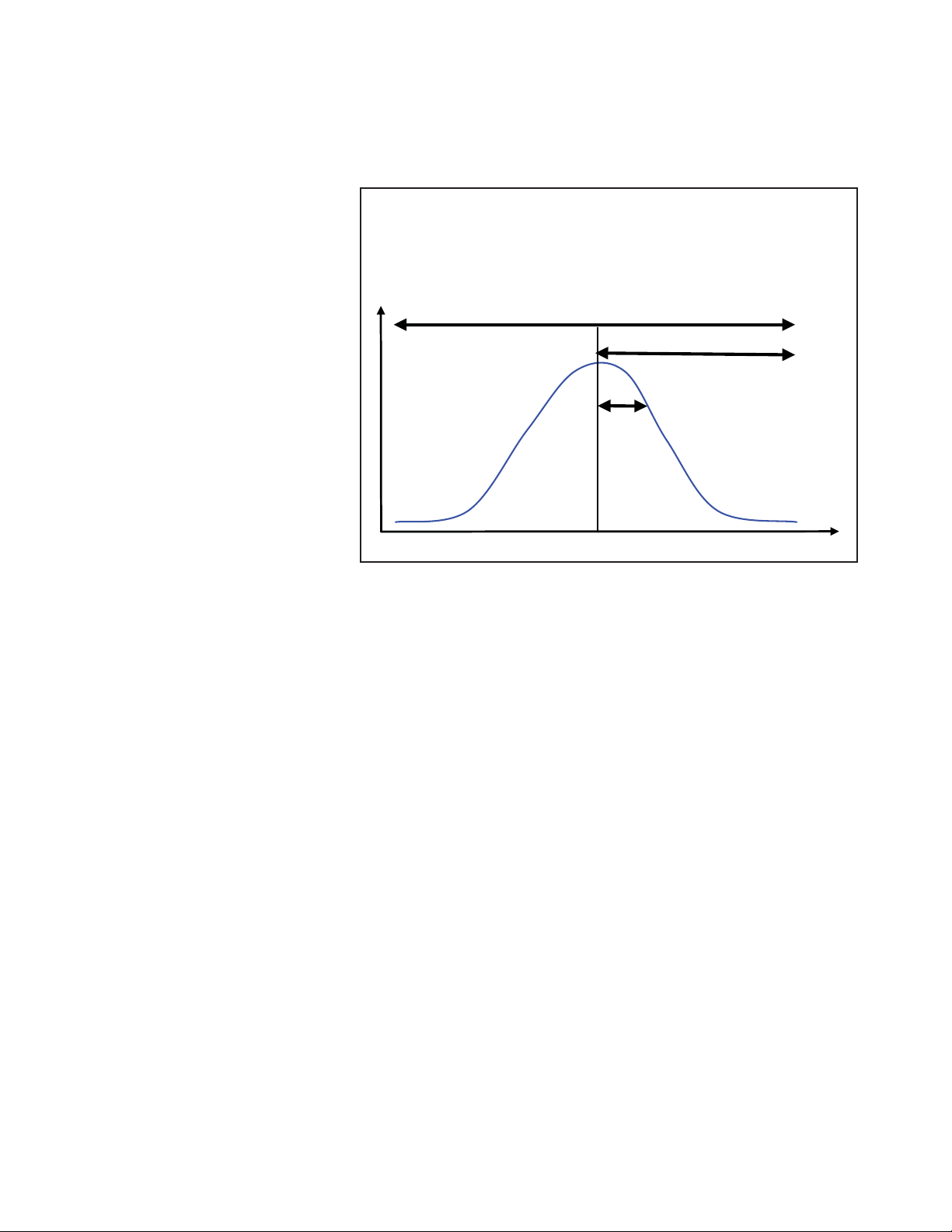
Voltage level crest factor
You can also select the crest factor out of 4 values – an indicator of signal quality –
using V
P/VRMS
or VPP/V
scales, depending on the standard to which you are testing.
RMS
The 81150A and the 81160A use the defi nition: crest factor = V
Voltage level crest factor
Voltage Level Crest Factor
V
pp
V
V
RM S
P/VRMS
P
Voltage
vo l t ag e
Pattern Generator – Test in
Addition to Analog, Digital
and Mixed Signal Devices
The result is noise that combines two extremes:
• Random and repeatable noise, for stress tests on one side
• While still being sufficiently random
Engineers working with serial buses or designers of analog, digital and mixed signal
devices require stressing their design with pattern. The optional Agilent 81150A and
81160A arbitrary bit shaped pattern generator allows sending ideal and real-world pattern.
The Agilent 81150A with arbitrary bit shaped pattern (Option PAT) allows emulating overshoot, asymmetric delay and duty cycle distortion up to 120 Mbit/s, the Agilent 81160A
up to 330 Mbit/s (Option 330) or even up to 660 Mbit/s (Option 660). Patterns can be
easily set up and distorted at your fingertips.
10
Page 11
Stress your device to its limits – defi ne your own bit shape
MOD
Emulate effects like...
• Capacitive load of the channel
• Asymmetric delay
• Crossing point deviations
• Duty cycle distortions
• Arbitrary transition times
• Level noise
• Delays from/to electrical idle
...By defi ning the transitions so that the
previous bit infl uences the current bit
PRBS
Sequencer
2-, 3- and 4-level signals
NRZ NRZ mode with minimum
transition times
NRZ mode with transition
Max voltage level
Min voltage level
time = 1/3 period
Mode
Data pattern: 01001101
Transition
Period
time
Arbitrary
Bit shape
Mode
NRZ mode with minimum
transition times
Bit shape waveforms
(user defined)
Output waveform
0→0
0→1
1→0
1→1
Max voltage level
Min voltage level
Max voltage level
Min voltage level
The 81150A and the 81160A pattern generators let you defi ne the transitions from one bit
to the other so that the previous bit infl uences the current bit. The user can set up own
defi ned arbitrary bit shapes.
In addition to user-defi ned patterns, standard patterns like PRBS up to 2
31
are available.
The sequencer allows setting up a pre-amble sequence so that the device under test
moves into test mode.
Additionally to 2-level signals, it is also possible to create 3- and even 4-level signals. With
the 3-level signals, it is no longer necessary to add different signals for electrical idle.
3-level signals are important e.g. for use in Ethernet environment and 4-level signals e.g.
for PAM4 applications.
Bit and block trigger mode
Pass through pattern for combined
physical and protocol test
up to 10 Mbit/s
Besides, standard trigger modes like continuous bit and block trigger modes allow adoptions to application needs. In the bit mode you see that on every trigger, the sequence
is advanced by one bit. An application example is a bit clock, which can be fed into an
external clock and then into the trigger input.
In the block mode the entire data block is generated once per trigger event. This is
interesting for example in applications with protocol data.
The 81150A and the 81160A pattern generators pass the data through to the device
under test and adopts it to any kind of stress test (shape and timing change).
Bridge the gap between protocol and physical layer test – in real time up to 10 Mbit/s
Increase your test efficiency by combining physical layer test with protocol test
81150A/81160A
Protocol
exerciser
Sends out protocol
data; e.g. VPT 1000
for FlexRay
IN
pass through
pattern
Real-time data pass
through with flexible
modulation and
re-stress test
Protocol handshake
DUT
Pass/fail test
The pass-through pattern functionality takes the protocol data via “mod in” and adopts it
to any kind of stress test (shape and timing changes).
11
Page 12

Modulation
Connectivity
Modulation of the pattern signal enables you to emulate real-world conditions.
AM – amplitude of the pattern signal is multiplied by the modulation signal to emulate
level distortions of the data signal e.g. sinusoidal interference.
FM – frequency of the pattern signal is modulated to emulate SSC on the data signal.
PM – the phase of the data bits is modulated to emulate jitter on the data signal.
Filling the arbitrary memory easily
There are several possibilities for fi lling the arbitrary memory. There are 6 built-in,
standard arbitrary waveforms, but you can also create any waveform you need, either on
the instrument or on a PC, using the Agilent 33503A BenchLink Waveform Builder Pro
software available for the 81150A and 81160A Pulse Function Arbitrary Noise Generators.
The 33503A software is being designed for waveform creation, waveform import from
Agilent scopes and waveform download to the 81150A and 81160A generators.
12
Page 13

Measurement –
Anywhere and Anytime
Channel 1: instrument view
The web interface allows you to use the full functionality and feature set of the Agilent
81150A and 81160A Pulse Function Arbitrary Noise Generators from a web browser.
Web interface
Channel 2
Just decide on the waveform
Web interface
Choose the crest factor / probability function you need
13
Page 14
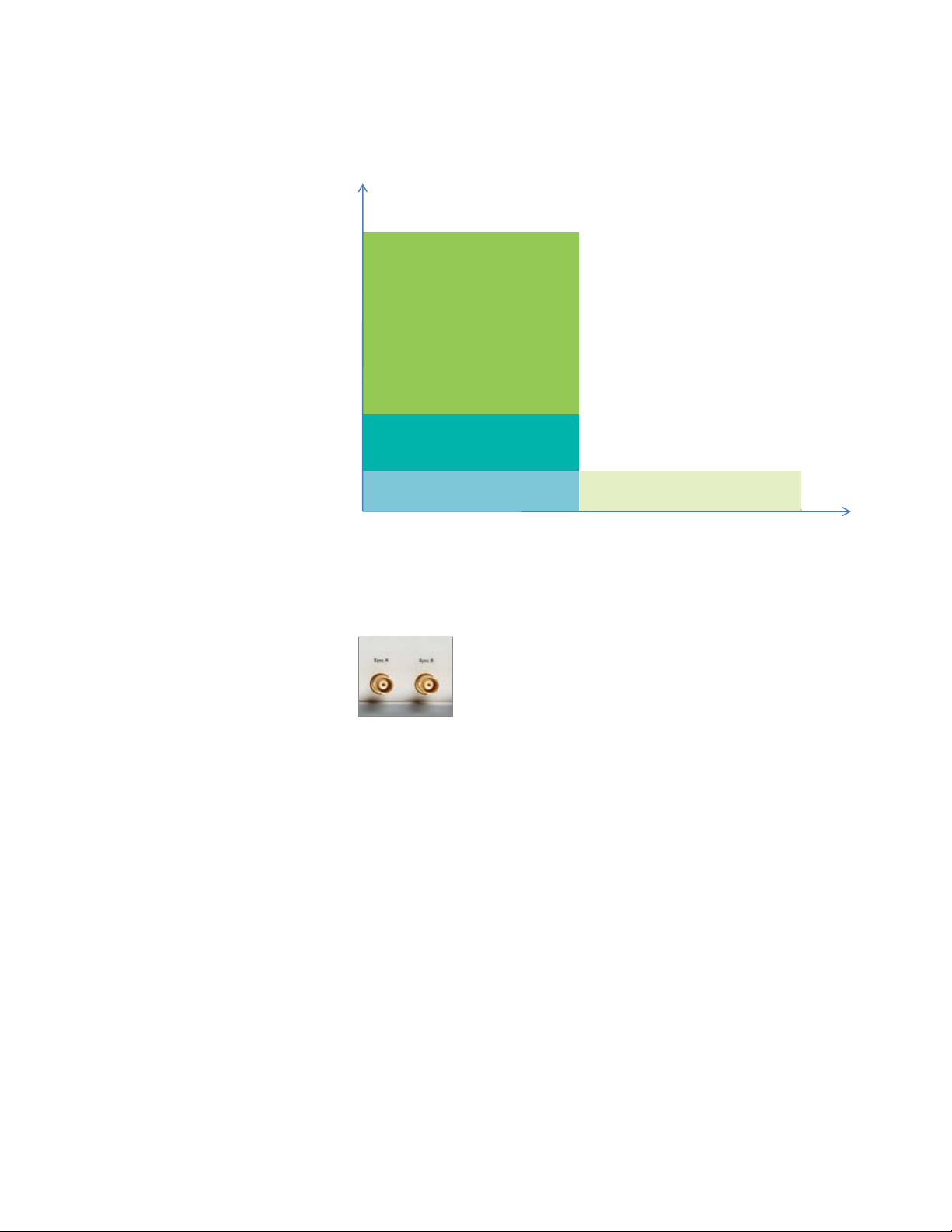
Amplifi er concept
50 MHz
330 MHz
Bandwidth
120 MHz
Different applications and devices call for different bandwidth and voltage levels. Choose
the performance you need.
81150A has a high bandwidth
amplifier and a hight voltage
amplifier, whereas the
81160A covers its whole
spectrum with only one
81160A
81150A high bandwidth amplifier
81150A high voltage amplifier
amplifier.
10 V5 V
Voltage
Flexible signal synchronization
The 81150A has one trigger output and one strobe output per channel.
The 81160A generates the trigger signal and the strobe signal per
channel internally. Using a fully configurable switch matrix, two of the
four internal signals can be routed to Sync Out A or Sync Out B.
81160A: Sync
Out A and B
14
Page 15

Modes of Operation
There are four components to the mode of operation:
• Coupling between channels
• Trigger mode
• Waveform type
• Advanced modes
Coupling between channel 1 and 2
Trigger modes
The two channel version has two distinct modes of operation:
• Coupling off: The two channels operate independently. Frequency generation for both
channels is based on the same clock reference, but can be selected independently.
• Coupling on: The frequency, trigger mode, waveform type and advanced mode are
identical for both channels. The fix delay of channel 1 and channel 2 is the same.
• Continuous: Continuous waveform, burst, sweep or modulation. The external in is not
used in continuous mode.
• Externally triggered: Each active transition at the external in (rising, falling or both)
generates a single waveform, burst or sweep.
• Externally gated: The active level (high or low) at the external in enables waveforms,
bursts or sweeps. The last waveform, burst or sweep is always completed.
• Internally triggered: The internal clock replaces the external trigger source. This can
be applied for waveform, burst, or sweep.
• Manual: This generates a single trigger. The source is either a button on the front
panel or a remote command.
Trigger rate (internally triggered)
81150A: 1 µHz to 120 MHz
81160A: 1 µHz to 330 MHz
Trigger rate (externally triggered)
81150A: DC to 120 MHz
81160A: DC to 330 MHz
15
Page 16

Waveform Types
• Standard waveforms: pulse, sine, square, ramp, noise, arbitrary
• Predefi ned arbitrary waveforms: exponential rise, exponential fall, sin(x)/x, cardiac and DC
• Pulse, sine, ramp, noise and arbitrary measured with 50 Ω source impedance into 50 Ω load impedance.
Pulse characteristics
81150A 81160A
Frequency range
High bandwidth amplifi er
High voltage amplifi er
Frequency resolution 1 μHz 1 μHz
Pulse width
Range
High bandwidth amplifi er
High voltage amplifi er
Resolution
Accuracy
Transition time
(independent rise and fall)
Range
High bandwidth amplifi er
High voltage amplifi er
Resolution
Accuracy
High bandwidth amplifi er
High voltage amplifi er
Overshoot 2% typ.
1) Overshoot disappears for transitions times > 5 ns (high bandwidth amplifi er) and > 15 ns (high voltage amplifi er).
2) Overshoot disappears for transition times > 2 ns.
1 μHz to 120 MHz
1 μHz to 50 MHz
4.1 ns to (period - 4.1 ns) typ.
10 ns to (period - 10 ns)
100 ps, 6 digits
± 500 ps ± 50 ppm
2.5 ns to 1000 s (10% to 90%)
7.5 ns to 1000 s (10% to 90%)
100 ps, 6 digits
± 500 ps ± 50 ppm
-1000 ps to +500 ps ± 50 ppm
(1)
1 μHz to 330 MHz
1.5 ns to (period - 1.5 ns) spec.
100 ps, 6 digits
± 300 ps ± 50 ppm
1.0 ns to 1000 s (10% to 90%)
100 ps, 6 digits
± 300 ps ± 50 ppm
4% typ.
(2)
Sine characteristics
81150A 81160A
Frequency range
High bandwidth amplifi er
High voltage amplifi er
Frequency resolution 1 μHz 1 μHz
Harmonic distortion
(High bandwidth amplifi er
50 Ω into 50 Ω)
Harmonic distortion
(High voltage amplifi er
50 Ω into 50 Ω)
Non-harmonic (spurious) distortion
SSB phase noise (10 kHz offset)
1 MHz
10 MHz
100 MHz
240 MHz
500 MHz
1 μHz to 240 MHz
1 μHz to 50 MHz
1 V
1 μHz to 2 MHz
2 MHz to 10 MHz
10 MHz to 35 MHz
35 MHz to 70 MHz
70 MHz to 240 MHz
1 μHz to 8 MHz
8 MHz to 50 MHz
PP
< -62 dBc spec. < -62 dBc spec.
< -57 dBc spec. < -52 dBc spec.
< -45 dBc spec. < -40 dBc spec.
< -35 dBc spec. < -30 dBc spec.
< -22 dBc spec. < -17 dBc spec.
10 V
PP
< -40 dBc
< -25 dBc
1 μHz to 20 MHz -60 dBc typ.
20 MHz to 200 MHz -55 dBc typ.
200 MHz to 240 MHz -50 dBc typ.
-119 dBc/Hz typ.
-115 dBc/Hz typ.
-93 dBc/Hz typ.
3 V
1 µHz to 500 MHz
PP
1 µHz to 2 MHz
2 MHz to 10 MHz
10 MHz to 50 MHz
50 MHz to 200 MHz
200 MHz to 500 MHz
1 μHz to 1 MHz -50 dBc typ.
1 MHz to 10 MHz -55 dBc typ.
10 MHz to 280 MHz -50 dBc typ.
280 MHz to 330 MHz -45 dBc typ.
330 MHz to 500 MHz -43 dBc typ.
-115 dBc/Hz typ.
-115 dBc/Hz typ.
-110 dBc/Hz typ.
-100 dBc/Hz typ.
1 V
PP
3 V
PP
< -65dBc spec. < -63 dBc spec.
< -62dBc spec. < -53 dBc spec.
< -50 dBc spec. < -40 dBc spec.
< -30 dBc spec. < -27 dBc spec.
< -22 dBc spec. < -20 dBc spec.
16
Page 17

Square characteristics
81150A 81160A
Frequency range
High bandwidth amplifi er
High voltage amplifi er
Frequency resolution 1 μHz 1 μHz
Duty cycle
High bandwidth amplifi er
High voltage amplifi er
Resolution 0.1% 0.1%
Transition time (10% to 90%)
High bandwidth amplifi er
High voltage amplifi er
Overshoot 2% typ. 4% typ.
1 μHz to 120 MHz
1 μHz to 50 MHz
(Freq/240 MHz) to 1 - (Freq/240 MHz)
e.g. 60 MHz; 25% to 75%
(Freq/100 MHz) to 1 - (Freq/100 MHz)
e.g. 1 MHz 1% to 99%
2.5 ns typ. fi xed
6 ns typ. fi xed
1 µHz to 330 MHz
(Freq/ 660 MHz) to 1 - (Freq/ 660 MHz)
e.g. 115 MHz; 25% to 75%
e.g. 3.3 MHz; 0.5% to 99.5%
1.1 ns typ. fi xed
Ramp characteristics
81150A 81160A
Frequency range 1 μHz to 5 MHz 1 µHz to 20 MHz
Frequency resolution 1 μHz 1 μHz
Linearity < 0.1% (f < 10 kHz) < 0.1% (f < 10 kHz)
Symmetry 0.0% to 100% 0.0% to 100%
Noise characteristics
81150A 81160A
Bandwidth
High bandwidth amplifi er
High voltage amplifi er
Amplitude distribution Selectable Gaussian,
Crest factor (peak/RMS) selectable 3.1, 4.8, 6.0, 7.0 typ.
Noise type Deterministic, triggerable Deterministic, triggerable
Repetition time ~ 26 days ~ 20 days
120 MHz typ.
40 MHz typ.
user defi ned
(Gaussian distribution)
160 MHz typ.
Selectable Gaussian,
user defi ned
3.1, 4.8, 6.0, 7.0 typ.
(Gaussian distribution)
17
Page 18

Arbitrary characteristics
81150A 81160A
DAC sample rate 2 GSa/s
Waveform length 2 to 512k points 1 channel instrument:
Wavelength vs. memory access rate 2 to 512k points at memory access rate
DAC resolution 14 bits 14 bits
Frequency range 1 μHz to 120 MHz 1 µHz to 330 MHz
Frequency resolution 1 μHz 1 μHz
Transition time (10% to 90%)
High bandwidth amplifi er
High voltage amplifi er
Filter bandwidth
High bandwidth amplifi er
High voltage amplifi er
PP jitter 1 ns typ. 400 ps typ. at memory sample rate
1) One step linear interpolation between two memory samples. DAC clock rate is 2,000 MSa/s.
2) Three steps linear interpolation between two memory samples. DAC clock rate is 2,500 MSa/s.
3) One step linear interpolation between two memory samples. DAC clock rate is 2,500 MSa/s
(1)
, fi xed 2.5 GSa/s, fi xed
1,000 MSa/s
1.7 ns typ.
5 ns typ.
240 MHz typ.
80 MHz typ.
2 to 256k points
2 channel instrument:
2 to 128k points
(1)
1 channel instrument, automatic selection:
128k to 256k points at memory access rate 625 MSa/s
64k to 128k points at memory access rate 1,250 MSa/s
2 to 64k points at memory access rate 2,500 MSa/s
2 channel instrument, automatic selection:
64k to 128k points at memory access rate 625 MSa/s
32 to 64k points at memory access rate 1,250 MSa/s
2 to 32k points at memory access rate 2,500 MSa/s
1.0 ns typ.
500 MHz typ.
2,500 MSa/s
(2)
(3)
(2)
(3)
18
Page 19

Advanced Modes
Three advanced modes exist:
• Modulation: selects the modulation type: AM, FM, PM, FSK, PWM
• Sweep: for frequency sweeps
• Bursts: repeats selected waveform n times
Modulation
A modulation input (for AM, FM, PM, FSK, PWM) for each channel is provided on the
back-panel. In the two channel instrument one channel can also modulate the other
channel.
Modulation In 1/modulation In 2
81150A 81160A
Input range (full scale) Selectable ±2.5 V or ±5 V ±2.5 V
Frequency range DC to 10 MHz DC to 10 MHz
Input impedance Selectable 10 kΩ, 50 Ω nom. Selectable 10 kΩ, 50 Ω nom.
Connector BNC, back panel BNC, back panel
AM
81150A 81160A
Carrier waveforms Sine, square, ramp, arbitrary Sine, square, ramp, arbitrary
Internal modulation Sine, square, ramp (up, 50%, down), noise,
arbitrary
Modulation frequency
Internal
External
Depth 0% to 120% 0% to 120%
Double-sideband suppressed carrier Selectable on/off Selectable on/off
Source Internal, external, channel Internal, external, channel
1 mHz to 10 MHz
DC to 10 MHz
Sine, square, ramp (up, 50%, down), noise,
arbitrary
1 mHz to 50 MHz
DC to 10 MHz
FM
81150A 81160A
Carrier waveforms Sine, square, ramp, arbitrary Sine, square, ramp, arbitrary
Internal modulation Sine, square, ramp (up, 50%, down), noise,
arbitrary
Modulation frequency
Internal
External
Deviation range 1 μHz to 240 MHz
Source Internal, external, channel Internal, external, channel
1 mHz to 10 MHz
DC to 10 MHz
(1)
Sine, square, ramp (up, 50%, down), noise,
arbitrary
1 mHz to 50 MHz
DC to 10 MHz
1 µHz to 500 MHz
(1)
PM
81150A 81160A
Carrier waveforms Sine, square, ramp, arbitrary Sine, square, ramp, arbitrary
Internal modulation Sine, square, ramp (up, 50%, down), noise,
arbitrary
Modulation frequency
Internal
External
Deviation range
Source Internal, external, channel Internal, external, channel
1) Max frequency depends on selected waveform.
1 mHz to 10 MHz
DC to 10 MHz
˚ 0 to 360˚
0 to 360
Sine, square, ramp (up, 50%, down), noise,
arbitrary
1 mHz to 50 MHz
DC to 10 MHz
19
Page 20

FSK
81150A 81160A
Carrier waveforms Sine, square, ramp, arbitrary Sine, square, ramp, arbitrary
Internal modulation 50% square 50% square
FSK rate
Internal
External
Frequency range 1 mHz to 240 MHz
Source Internal, external, channel Internal, external, channel
1) Max frequency depends on selected waveform.
2) For export control: Effective switching time is 40 ns.
1 mHz to 50 MHz
1 mHz to 10 MHz
(1) (2)
1 mHz to 50 MHz
1 mHz to 10 MHz
1 mHz to 500 MHz
(1)
PWM
81150A 81160A
Carrier waveform Pulse Pulse
Internal modulation Sine, square, ramp (up, 50%, down), noise,
arbitrary
Modulation frequency
Internal
External
1 mHz to 10 MHz
DC to 10 MHz
Deviation range 0% to 100% of pulse width 0% to 100% of pulse width
Source Internal, external, channel Internal, external, channel
Sine, square, ramp (up, 50%, down), noise,
arbitrary
1 mHz to 50 MHz
DC to 10 MHz
Sweep
An independent frequency sweep is provided for each channel.
81150A 81160A
Waveforms Pulse, sine, square, ramp, triangle, arbitrary Pulse, sine, square, ramp, triangle, arbitrary
Type Linear or logarithmic Linear or logarithmic
Direction Up or down Up or down
Sweep time 100 μs to 500 s 50 μs to 500 s
Start frequency/stop frequency 1 μs to 240 MHz
(1)
1 μHz to 500 MHz
(1)
Amplitude fl atness (relative to 1 kHz, 2 VPP) — 1 μHz to 500 MHz ±0.5 dB typ.
Trigger source External, internal, manual External, internal, manual
Marker Frequency marker Frequency marker
1) Max frequency depends on selected waveform.
Burst
An independent frequency sweep is provided for each channel.
81150A 81160A
Waveforms Pulse, sine, square, ramp, triangle, arbitrary Pulse, sine, square, ramp, triangle, arbitrary
Frequency 1 μHz to 120 MHz 1 µHz to 330 MHz
Modes Externally triggered, internally triggered, externally
gated
# of waveforms in a burst 2 to 2
31
- 1 (~ 2 billion) 2 to 231 - 1 (~ 2 billion)
Trigger period 16.7 ns to 9999 s 6.1 ns to 9999s
Start phase
(1)
-360 to +360
˚ -360 to +360˚
Gate source External External
Trigger source External, internal, manual External, internal, manual
1) Available for all waveforms except pulse, square and ramp.
Externally triggered, internally triggered, externally
gated
20
Page 21

Outputs
Main outputs
A selectable single-ended or differential output is provided for each channel on
the front-panel.
Max. frequency
81150A 81160A
High bandwidth amplifi er 120 MHz pulse/240 MHz sine 330 MHz pulse/500 MHz sine
High voltage amplifi er 50 MHz
Out 1/Out 2
81150A 81160A
Output type Single-ended or differential Single-ended or differential
Amplitude (50 Ω into 50 Ω)
High bandwidth amplifi er
1 μHz to 120 MHz
120 MHz to 240 MHz
50 mVPP to 5 V
50 mVPP to 3V
1 µHz to 330 MHz
330 MHz to 500 MHz
High voltage amplifi er
1 μHz to 50 MHz
100 mVPP to 10 V
Amplitude (50 Ω into open, 5 Ω into 50 Ω)
High bandwidth amplifi er
1 μHz to 120 MHz
120 MHz to 240 MHz
100 mV
100 mVPP to 5 V
1 µHz to 60
High voltage amplifi er
1 μHz to 50 MHz
200 mVPP to 20 V
DC amplitude accuracy ± (1.5% of setting + 5 mV) ± (1.5% of setting + 5 mV)
Voltage window (50 Ω into 50 Ω)
High bandwidth amplifi er
High voltage amplifi er
-5 V to +5 V typ.
-10 V to +10 V typ.
Voltage window (50 Ω into open,
5 Ω into 50 Ω)
High bandwidth amplifi er
High voltage amplifi er
-10 V to +10 V
-20 V to +20 V typ.
DC offset accuracy
± 5 V voltage window
± 10 V voltage window
± 20 V voltage window
± (25 mV + 1%)
± (50 mV + 1%)
± (75 mV + 1%)
Resolution 1 mV, 4 digits 1 mV, 4 digits
Output impedance Selectable 50 Ω / 5 Ω typ. 50 Ω nom.
Variable load impedance 0.3 Ω to 1 MΩ
Protection Short-circuit protected, overload disables
main output
Connector BNC, front panel BNC, front panel
1) All amplitudes are single-ended amplitudes. Differential peak-peak amplitudes are twice the single-ended value.
2) 10 VPP for 50 Ω into open; 9 VPP for 5 Ω into 50 Ω.
3) Current of normal Out plus current of complement Out is limited to 440 mA per channel.
4) Only for 50 Ω into open.
to 10 V
PP
(1)
typ.
PP
(1)
typ.
PP
(1)
typ.
PP
(1)
(to 9 V
PP
(1)
PP
(1)
PP
(1)
(-9 V to +9 V
(3)
50 mVPP to 5 V
50 mVPP to 3 V
(2)
)
PP
100 mVPP to 10 V
PP
PP
(1)
(1)
PP
spec.
spec.
(1) (4)
-5 V to +5 V spec.
(2)
) typ.
- 10 V to + 10 V spec.
(4)
±(25 mV + 1%)
± (50 mV + 1%)
0.1 Ω to 1 MΩ
Short-circuit protected, overload disables
main output
21
Page 22

Clock Reference
External reference output
81150A 81160A
Frequency
Accuracy
Stability
Aging
Output level 1 V nom. 1 V nom.
Impedance 50 Ω nom., AC coupled 50 Ω nom., AC coupled
Connector BNC, rear panel BNC, rear panel
External reference input
Lock range 10 MHz ± 500 ppm 10 MHz ± 500 ppm typ.
Input level 200 mVpp to 5 V
Impedance 1 kΩ nom., AC coupled 1 kΩ nom., AC coupled
Connector BNC, rear panel BNC, rear panel
Internal frequency characteristics
Accuracy ± 50 ppm ±10 ppm
Stabilty ± 2 ppm, 0 to 50 ºC ± 2 ppm, 0 to 55 ºC
Aging ± 1 ppm per year ± 1 ppm per year
10 MHz typ.
± 50 ppm
± 2 ppm, 0 to 50 ºC
± 1 ppm per year
10 MHz spec.
± 10 ppm
± 2 ppm, 0 to 55 °C
± 1 ppm per year
81150A 81160A
pp
200 mVPP to 5 VPP typ.
81150A 81160A
External Input
A common external input is provided for both channels on the front panel. The external
input is used for external trigger or external gate modes.
81150A 81160A
Frequency range DC to 120 MHz DC to 330 MHz
Input range -10 V to +10 V - 5 V to + 5 V
Maximum input amplitude 10 V
Input sensitivity 200 mV
Threshold
Range
Resolution
Impedance Selectable 10 kΩ /50 Ω, DC coupled Selectable, 1 kΩ/ 50 Ω, DC coupled
Slope Selectable, rising/falling/both Selectable, rising/falling/both
Pulse width > 3.3 ns > 1.3 ns
Transition time < 100 ns
Connector BNC, front panel BNC, front panel
Frequency counter
Gate time, up to 330 MHz — 1 s, fi x
Accuracy — See clock reference specifi cations
PP
PP
-10 V to 10 V
100 mV
The frequency applied to external input is measured
10 V
PP
Hysteresis low: 200 mV
Hysteresis high: 350 mV
- 5 V to + 5 V
100 mV
PP
PP
22
Page 23

81150A Trigger Outputs
For 81150A, a separate trigger output is provided for each channel on the front-panel.
In advanced mode internally/externally modulated (AM, FM, PM, PWM), the trigger
output has the frequency of the unmodulated carrier waveform, with a 50% duty cycle.
For FSK modulation, the trigger output has the same frequency as the data output.
That is, it alternates between the two frequencies.
If noise is selected, a trigger signal is generated when noise is restarted
internally, externally or manually.
For all other modes of operation the trigger signal (TRIGGER OUT) marks the start of each
waveform period.
81150A Trigger Out 1/Trigger Out 2
81150A
Output level
TTL
ECL
Pulse width
Internally triggered, continuous
Externally triggered
Transition time (20% to 80%) 2.0 ns typ.
Maximum rate 120 MHz
Impedance 50 Ω nom.
Connector BNC, front panel
1) For output frequencies > 120 MHz, the trigger rate is ¼ of the output frequency. If a frequency sweep or a FSK
frequency exceeds 120 MHz, the trigger rate is ¼ of the output frequency.
Selectable TTL/ECL
0 V / 2.5 V nom.
-0.85 V/-1.80 V nom.
50% duty cycle typ.
4 ns typ.
(1)
81150A Strobe Outputs
A strobe output is provided for each channel on the front-panel of pulse generator 81150A. The
strobe output signal has a different function, depending on the mode of operation.
If no advanced mode is selected, the strobe output is a constant low.
In advanced mode internal/external triggered or gated burst, the strobe output provides a
signal indicating the duration of a burst. The rising edge of the strobe signal is synchronized to
the start of the fi rst waveform period in a burst. The falling edge is synchronized to the start of
the last waveform period in the burst.
In advanced mode sweep with the frequency marker off, the strobe output is a pulse with
half the duration of the sweep. The strobe signal goes high at the beginning of the sweep.
In advanced mode sweep with the frequency marker on, the strobe output goes high at the
beginning of the sweep and goes low at the marker frequency.
In pattern mode (block mode = On), the strobe output goes high at the beginning of the
pattern and goes low at the last bit of the pattern. Refer to the User Guide for more details.
In advanced mode internally/externally modulated (AM, FM, FSK, PM, PWM), the strobe
output is the analog modulation waveform.
In pattern mode (block mode = On), the logical strobe signal goes high at the beginning of the
pattern and goes low at the last bit of the pattern. Refer to the User Guide for more details.
81150A Strobe Out 1/Strobe Out 2
81150A
Digital output level
TTL
ECL
Analog output level (modulator)
Impedance 50 Ω nom.
Connector BNC, front panel
Min pulse width 4 ns typ.
Transition time (20% to 80%) 2.0 ns typ.
Selectable TTL/ECL
0 V/2.5 V nom.
-0.85 V/-1.80 V nom.
-2.0 V to 2.0 V (full scale)
23
Page 24

81160A Trigger and Strobe
Outputs Sync Out A and
Sync Out B
For the one channel instrument as well as the two channel instrument two high speed
outputs Sync Out A and Sync Out B are provided at the front panel. The Sync output
signals can be confi gured very fl exible by an internal switch matrix to output the logical
Trigger Out functionality or Strobe Out functionality according to the following switch
matrix.
1 channel instrument
81160A
Sync Out A source None, logical trigger signal 1, logical strobe signal 1
Sync Out B source None, logical trigger signal 1, logical strobe signal 1
1) It is e.g. possible, that the logical trigger signal 1 functionality is routed simultaneously to Sync Out A and
Sync Out B.
2 channel instrument
81160A
Sync Out A source None, logical trigger signal 1, logical strobe signal 1,
logical trigger signal 2, logical strobe signal 2
Sync Out B source None, logical trigger signal 1, logical strobe signal 1,
logical trigger signal 2, logical strobe signal 2
1) It is e.g. possible, that the logical trigger signal 1 functionality is routed simultaneously to Sync Out A and
Sync Out B.
Sync Out A/Sync Out B
81160A
Digital output level
TTL
ECL
Analog output level (modulator)
Impedance 50 Ω nom.
Transition time 0.8 ns typ. (20%/80%)
Connector BNC, front panel
Selectable TTL, ECL
0 V/2.5 V nom.
-0.85 V/-1.80 V nom.
-2.0 V to 2.0 V (full scale),
Available, if routed to logical Strobe Out
The logical trigger output and logical strobe output functionality is described below.
Logical trigger signal
The logical trigger signal is an internally generated signal that can be routed to the BNC
connector of Sync Out A or Sync Out B. For the two channel instrument, the logical trigger
signal is generated for both, channel 1 and channel 2.
In advanced mode internally/externally modulated (AM, FM, PM, PWM), the logical
trigger signal has the frequency of the unmodulated carrier waveform with 50% duty cycle.
For FSK modulation the logical trigger signal generates the same frequency as the data
output – it alternates between the two frequencies.
If noise is selected, a trigger signal is generated when noise is restarted internally,
externally or manually.
For all other modes of operation the logical trigger signal marks the start of each
waveform period.
24
Page 25

Logical trigger signal 1/logical trigger signal 2
81160A
Pulse width
Internallly triggered, continuous
Externally triggered
Maximum rate 330 MHz
1) For output frequencies > 330 MHz, the trigger rate is ½ of the output frequency. In pattern mode with bit rate
> 330 MBit/s, the trigger rate is ½ of the output frequency. If a frequency sweep or a FSK frequency exceeds
330 MHz, the trigger rate is ½ of the output frequency.
50% duty cycle typ.
1.5 ns typ.
(1)
Logical strobe signal
The logical strobe signal is an internally generated signal that can be routed to the BNC
connector of Sync Out A or Sync Out B. For the two channel instrument, the logical strobe
signal is generated for both, channel 1 and channel 2.
The logical strobe signal has a different function, depending on the mode of operation.
If no advanced mode is selected, the logical strobe signal is constant low.
In advanced mode internal/external triggered or gated burst, the logical strobe signal
provides a signal indicating the duration of a burst. The rising edge of the logical strobe
signal is synchronized to the start of the fi rst waveform period in a burst. The falling edge
is synchronized to the start of the last waveform period in the burst.
In advanced mode sweep with the frequency marker off, the logical strobe signal is a
pulse with half of the duration of the sweep. The strobe signal goes high at the beginning
of the sweep.
In advanced mode sweep with the frequency marker on, the logical strobe signal goes
high at the beginning of the sweep and goes low at the marker frequency.
In advanced mode internally/externally modulated (AM, FM, FSK, PM, PWM), logical
strobe signal is the analog modulation waveform.
In pattern mode (block mode=On), the logical strobe signal goes high at the beginning
of the pattern and goes low at the last bit of the pattern. Refer to the User Guide for more
details.
25
Page 26

Digital Channel Addition
If the instrument is equipped with two output channels, channel 2 can be added to
channel 1 internally. The maximum output voltage of channel 1 remains unchanged. If
channel addition is selected, channel 2 outputs the unchanged waveform of channel 2.
Timing Characteristics
External In timing characteristics
81150A 81160A
Delay: External In to Main Out 1, 2
Fix delay
Advance mode: off, burst
Advanced mode: sweep
Pattern mode: on
Variable delay
Range
Resolution
Accuracy
Delay
Fix delay
Advanced mode: off, burst
Advanced mode: sweep
Pattern mode: on
Jitter
External In to Main Out 1, 2
External In to Trigger Out 1, 2
External In to Strobe Out 1, 2
External In to Sync Out A, B
1) Not available, if sweep or modulation is selected
2) Trigger period ≥ variable delay
3) External in amplitude > 500 mV. External in transition time < 10 ns. Valid for externally triggered pulse,
square, sine, ramp, arb. Externally triggered noise or externally triggered sweep has peak-peak jitter of 8 ns
for the 81150A and 3.2 ns for the 81160A, measured with 50 Ω source impedance at main output.
(1)
(3)
366 ns typ.
350 ns typ.
406 ns typ.
Independent for Out 1, Out 2
0 s to 1000 s
1 ps, 6 digits
± 25 ps ± 50 ppm
External In to Trigger Out 1, 2
366 ns typ.
350 ns typ.
406 ns typ.
15 ps RMS typ.
15 ps RMS typ.
15 ps RMS typ.
―
(2)
404 ns typ.
404 ns typ.
404 ns typ.
Independent for Out 1, Out 2
0 s to 1000 s
1 ps, 6 digits
± 35 ps ± 50 ppm
External In to Sync Out A, B
404 ns typ.
404 ns typ.
404 ns typ.
15 ps RMS typ.
―
―
15 ps RMS typ.
(2)
26
Page 27

Continuous or internally triggered timing characteristics
81150A 81160A
Delay
Fix delay
Variable delay Out 1, 2
Range in continuous mode
(1)
(2)
Range in internally triggered mode
Resolution
Accuracy
Delay
Advanced mode: burst
(4)
Jitter
1) Not available, if sweep or modulation is selected.
2) Advanced mode = off or advanced mode = burst .
3) Trigger period ≥ variable delay.
4) Measured with 50 Ω source impedance at Main Out. Valid for continuous or internally triggered pulse, square, sine, ramp, arb.
Internally triggered or continuous noise or sweep has peak-peak jitter of 8 ns typ. for the 81150A and 3.2 ns for the 81160A.
Trigger Out 1, 2 to Main Out 1, 2
0 ns typ.
Independent for Out 1, Out 2
0 to 1 waveform period
(3)
0 s to 1000 s typ.
1 ps, 6 digits
± 25 ps ± 50 ppm
Trigger Out 1, 2 to Strobe Out 1, 2
0 ns typ.
Jitter
Main Out 1, 2 to Main Out 1, 2: 7 ps RMS typ.
Trigger Out 1, 2 to Main Out 1, 2: 8 ps RMS typ.
Trigger Out 1, 2 to Strobe Out 1, 2: 9 ps RMS typ.
Trigger Out 1, 2 to Trigger Out 1, 2: 9 ps RMS typ.
Sync Out A, B to Main Out 1,2
0 ns typ.
Independent for Out 1, Out 2
0 to 1 waveform period
0 s to 1000 s spec.
1 ps, 6 digits
± 35 ps ± 50 ppm
Sync Out A to Sync Out B
0 ns typ.
Jitter
Main Out 1, 2 to Main Out 1, 2: 7 ps RMS typ.
Sync Out A, B to Main Out 1, 2: 8 ps RMS typ.
Sync Out A to Sync Out B: 9 ps RMS typ.
Coupled mode on timing characteristics
Delay: Main Out 1 to Main Out 2
Fix delay
Variable delay Out 1, 2
Range in continuous mode
Range in internally triggered mode
(1)
(2)
(3)
Resolution
Accuracy
1) Not available, if sweep or modulation is selected.
2) Advanced mode = off or advanced mode = burst .
3) Trigger period ≥ variable delay.
81150A 81160A
0 ns typ.
Independent for Out 1, Out 2
0 to 1 waveform period
0 s to 1000 s typ.
1 ps, 6 digits
± 25 ps ± 50 ppm
0 ns typ.
Independent for Out 1, Out 2
0 to 1 waveform period
0 s to 1000 s spec.
1 ps, 6 digits
± 35 ps ± 50 ppm
27
Page 28

Pattern generator (optional)
81150A
Option PAT
Data rate 1 μbit/s to 120 Mbit/s
(with internal pattern source)
Pattern memory 16 Mbit with 1 bit resolution 4 Mbit for 1 channel instrument
Pattern memory
resolution
Number of levels 2, 3, or 4 (user selectable)
Sequencing Preamble followed by one looped data block—loop count:
1 - 10,000,000 the whole sequence can loop indefi nitely or triggered
Trigger modes Continuous, gated, one bit per trigger event, one sequence per trigger event
Pattern sources Internal: PRBS -7, 9, 11, 15, 23, and 31
External: Pass through pattern mode. Pattern is applied and sampled at Modulation In. Indefi nite pattern length.
Up to 10 Mbit/s. Selectable automatic sampling for asynchronous operation or fi xes sampling for
External sampling Automatic and fi x
Pattern modulation AM, FM, PM
Arbitrary bit shapes User defi ned and predefi ned bit transitions with up to 64 arbitrary waveform points per bit transitions
81160A
Option 330
1 µbit/s to 330 Mbit/s 1 µbit/s to 660 Mbit/s
2 Mbit per channel for 2 channel instrument
1 bit 1 bit for data rate 1 μbit/s to 330 Mbit/s
User-defi ned
synchronous operation
81160A
Option 660
2 bits for data rate 330 Mbit/s to 660 Mbit/s
28
Page 29

Download Times
Block transfer is the fastest way to download waveforms to both the Agilent 81150A and
81160A Pulse Function Arbitrary Noise Generators.
Download times: block transfer (meas.)
81150A 81160A
USB 2.0 GPIB LAN USB 2.0 GPIB LAN
1 k points 31 ms typ. 35 ms typ. 35 ms typ. 23 ms typ. 44 ms typ. 27 ms typ.
8 k points 65 ms typ. 120 ms typ. 80 ms typ. 68 ms typ. 198 ms typ. 86 ms typ.
64 k points 700 ms typ. 1 s typ. 730 ms typ. 330 ms typ. 1.36 s typ. 449 ms typ.
256 k points 1.25 s typ. 5.4 s typ. 1.75 s typ.
512 k points 2.9 s typ. 5.2 s typ. 3.7 s typ.
Download times: integer comma separated values (meas.)
81150A 81160A
USB 2.0 GPIB LAN USB 2.0 GPIB LAN
1 k points 220 ms typ. 200 ms typ. 220 ms typ. 214 ms typ. 188 ms typ. 181 ms typ.
8 k points 1.8 s typ. 1.6 s typ. 1.4 s typ. 1.6 s typ. 1.45 s typ. 1.39 s typ.
64 k points 14.2 s typ. 12.6 s typ. 12 s typ. 13.0 s typ. 11.5 s typ. 11.0 s typ.
Download times: fl oat comma separated values (meas.)
81150A 81160A
USB 2.0 GPIB LAN USB 2.0 GPIB LAN
1 k points 290 ms typ. 280 ms typ. 270 ms typ. 297 ms typ. 256 ms typ. 236 ms typ.
8 k points 2.4 s typ. 2.1 s typ. 1.9 s typ 2.23 s typ. 1.98 s typ. 1.8 s typ
64 k points 20 s typ. 16 s typ. 15 s typ. 18.2 s typ. 15.7 s typ. 14.3 s typ.
29
Page 30

General Specifi cations
81150A 81160A
Power supply 100 V to 240 V ~, 50 to 60 Hz
100 V to 127 V ~, 50 to 400 Hz
Power consumption 110 W nom. 90 W nom.
Operating temperature 0 to 50 ºC 0 to 55 ºC
Operating altitude Up to 2000 m Up to 2000 m
Storage temp. -40 to 70 °C -40 to 70 °C
Stored states 4 named user confi gurations and factory default 4 named user confi gurations and factory default
Power on state Default or last state Default or last state
Interface 2 x USB 2.0 standard A,
1 x USB 2.0 standard B,
GPIB and LAN
Programming language SCPI-1997
IEEE-488.2
LXI compliant to LXI class C (rev. 1.1)
Dimensions (WxHxD)
Bench top
Rack mount
Weight 8 kg 8 kg
Safety designed to IEC61010-1
EMC tested to IEC61326 IEC61326
Warm up time 30 min. 30 min.
Calibration interval 2 years recommended 2 years recommended
Warranty 1 year standard 1 year standard
Cooling requirements When operating the instrument choose a location that
439 mm x 108 mm x 456 mm
428 mm x 89 mm x 439 mm
UL61010
CSA22.2 61010.1 certifi ed
provides at least 80 mm of clearance at rear, and at
least 30mm of clearance at each side
100 V to 240 V ~, 50 to 60 Hz
100 V to 127 V ~, 50 to 400 Hz
2 x USB 2.0 standard A,
1 x USB 2.0 standard B,
GPIB and LAN
SCPI-1997
IEEE-488.2
LXI compliant to LXI class C (rev. 1.1)
439 mm x 108 mm x 456 mm
428 mm x 89 mm x 439 mm
IEC61010-1
UL61010
CSA22.2 61010.1 certifi ed
When operating the instrument choose a location that
provides at least 80 mm of clearance at rear, and at
least 30mm of clearance at each side
Defi nitions
Specifi cation (spec.)
The warranted performance of a calibrated instrument that has been stored for a minimum of 2 hours within the operating temperature
range of 0 °C to 55 °C and after a 45-minute warm up period. Within ± 10 °C after autocal. All specifi cations include measurement
uncertainty and were created in compliance with ISO-17025 and Z540 methods. Data published in this document are specifi cations (spec)
only where specifi cally indicated.
Typical (typ.)
The characteristic performance, which 80% or more of manufactured instruments will meet. This data is not warranted, does not include
measurement uncertainty, and is valid only at room temperature (approximately 23 °C).
Nominal (nom.)
The mean or average characteristic performance, or the value of an attribute that is determined by design such as a connector type,
physical dimension, or operating speed. This data is not warranted and is measured at room temperature (approximately 23 °C).
Measured (meas.)
An attribute measured during development for purposes of communicating the expected performance. This data is not warranted and is
measured at room temperature (approximately 23 °C).
Accuracy
Represents the traceable accuracy of a specifi ed parameter. Includes measurement error and timebase error, and calibration source
uncertainty.
30
Page 31

Available Modes
of Operation
Continuous
81150A and 81160A
Pulse Square Sine Ramp Noise Arb DC
Advanced mode: off YYYYYYY
Advanced mode: burst YYYYNYN
Advanced mode:
Modulation
Advanced mode: sweep NYYYNYN
AM N Y Y Y N Y N
FM N Y Y Y N Y N
PM N Y Y Y N Y N
FSK N Y Y Y N Y N
PWM Y N N N N N N
Internally triggered or externally triggered
81150A and 81160A
Pulse Square Sine Ramp Noise Arb DC
Advanced mode: off YYYYYYN
Advanced mode: burst YYYYNYN
Advanced mode:
Modulation
AM N N N N N N N
FM N N N N N N N
PM N N N N N N N
FSK N N N N N N N
PWM N N N N N N N
Advanced mode: sweep NYYYNYN
Gated
81150A and 81160A
Pulse Square Sine Ramp Noise Arb DC
Advanced mode: off YYYYYYN
Advanced mode: burst YYYYNYN
Advanced mode:
Modulation
Advanced mode: sweep NYYYNYN
AM N N N N N N N
FM N N N N N N N
PM N N N N N N N
FSK N N N N N N N
PWM N N N N N N N
31
Page 32

Ordering Information for
811
50
A
Agilent 81150A
#001 1-channel pulse function arbitrary noise generator
#002 2-channel pulse function arbitrary noise generator
#1A7
ISO17025 calibration documents
#Z54 Z540.3 calibration documents
#PAT License for 120 Mbit/s pattern generator
Accessories included
• Certificate of calibration
• Local power cord
• USB cable
• Product CD (User Guide, Getting Started Guide, IVI-COM driver, examples for remote
access)
Optional accessories
#DOC Printed documentation. Includes printed Getting Started Guide and printed
User Guide
#1CP Rack mount kit
#R1280A Additional 2-years warranty (3-years total)
Upgrades for 81150A
81150AU
#PAT License for pattern generator
#DOC Printed documentation
#EHD Fixture for 100 Mbit Ethernet and HDMI 1.4
32
Page 33

Ordering Information for
811
60
A
Agilent 81160A
#001 1-channel pulse function arbitrary noise generator
#002 2-channel pulse function arbitrary noise generator
#1A7
ISO17025 calibration documents
#Z54 Z540.3 calibration documents
#330 License for 330 Mbit/s pattern generator
#660 License for 660 Mbit/s pattern generator
Accessories included
• Certificate of calibration
• Local power cord
• USB cable
• Product CD (User Guide, Getting Started Guide, IVI-COM driver, examples for remote
access)
Optional accessories
#DOC Printed documentation. Includes printed Getting Started Guide and printed
User Guide
#1CP Rack mount kit
#R1280A Additional 2-years warranty (3-years total)
Upgrades for 81160A
81160AU
#330 License for 330 Mbit/s pattern generator
#660 License for 660 Mbit/s pattern generator
#326 License for upgrade from 330 Mbit/s to 660 Mbit/s pattern generator
#DOC Printed documentation
33
Page 34

Literature title Publication
s
number
Pulse Pattern and Data
Generators Brochure
81150A and 81160A Pulse
5980-0489E
5989-7718EN
Function Arbitrary Noise
Generator Demo Guide
81150A Pulse Function
5989-7720EN
Arbitrary Noise Generator
Flyer
81150A and 81160A Pulse
5989-7860EN
Function Arbitrary Noise
Generator Application
Booklet
81150A Quick Fact Sheet
81160A Quick Fact Sheet
33503A BenchLink
5990-4565EN
5990-6984EN
5990-7569EN
Waveform Builder Pro
Software Data Sheet
For the latest version of this document,
please visit our website at:
www.agilent.com/find/81150
www.agilent.com/find/81160
and go to the Product Library.
www.lxistandard.org
LAN eXtensions for Instruments puts
the power of Ethernet and the Web
inside your test systems. Agilent
is a founding member of the LXI
consortium.
Agilent Advantage Services is committed
to your success throughout your equipment’s lifetime. To keep you competitive,
we continually invest in tools and
processes that speed up calibration and
repair and reduce your cost of ownership.
You can also use Infoline Web Services
to manage equipment and services more
effectively. By sharing our measurement
and service expertise, we help you create
the products that change our world.
www.agilent.com/find/advantageservices
Agilent Electronic Measurement Group
DEKRA Certified
ISO 9001:2008
Quality Management SystemQuality Management Sy
www.agilent.com/quality
Agilent Channel Partners
www. agilent.com/find/channelpartners
Get the best of both worlds: Agilent’s
measurement expertise and product
breadth, combined with channel
partner convenience.
Agilent Email Updates
www.agilent.com/find/emailupdates
Get the latest information on the
products and applications you select.
www.agilent.com
www.agilent.com/fi nd/81150
www.agilent.com/fi nd/81160
For more information on Agilent Technologies’ products, applications or services,
please contact your local Agilent office. The
complete list is available at:
www.agilent.com/fi nd/contactus
Americas
Canada (877) 894 4414
Brazil (11) 4197 3600
Mexico 01800 5064 800
United States (800) 829 4444
Asia Pacifi c
Australia 1 800 629 485
China 800 810 0189
Hong Kong 800 938 693
India 1 800 112 929
Japan 0120 (421) 345
Korea 080 769 0800
Malaysia 1 800 888 848
Singapore 1 800 375 8100
Taiwan 0800 047 866
Other AP Countries (65) 375 8100
Europe & Middle East
Belgium 32 (0) 2 404 93 40
Denmark 45 45 80 12 15
Finland 358 (0) 10 855 2100
France 0825 010 700*
*0.125 €/minute
Germany 49 (0) 7031 464 6333
Ireland 1890 924 204
Israel 972-3-9288-504/544
Italy 39 02 92 60 8484
Netherlands 31 (0) 20 547 2111
Spain 34 (91) 631 3300
Sweden 0200-88 22 55
United Kingdom 44 (0) 118 927 6201
For other unlisted countries:
www.agilent.com/fi nd/contactus
Revised: October 11, 2012
Product specifications and descriptions
in this document subject to change
without notice.
© Agilent Technologies, Inc. 2011-2013
Published in USA, January 28, 2013
5989-6433EN
 Loading...