

Page 1
Agilent 81110A
Agilent 81100 Family of
Pulse Pattern Generators
Data Sheet – Version 1.3
Signals for testing digital designs and
components
The Agilent 81101A, 81104A, 81110A and 81130A generate all
the standard pulses and digital patterns needed to test current
logic technologies (CMOS, TTL, LVDS, ECL, etc.).
With the optional second channel on all of the models from
80 MHz to 660 MHz, multi-level and multi-timing signals can
be obtained using the internal channel addition feature.
• Variable pulse parameters in pattern mode as well as in
pulse mode (not on the 81130A)
• Synchronously triggerable
• Simulation of reflections/distortions
• (81104A, 81110A)
• Three/four-level codes (81104A, 81110A)
Flexible Pulses or Patterns for Digital
Designs – Key Features
• Pattern mode on all models from 80 MHz to 660 MHz,
including pseudo-random binary sequence
• The outputs of dual-channel instruments can be added
(analog or EXOR, depending on model)
• User-retrofittable channels for most models
• Upward compatibility
• Individual solutions for frequencies up to 50, 80, 165, 330,
400 and 660 MHz
• 100% form/fit compatibility
Page 2

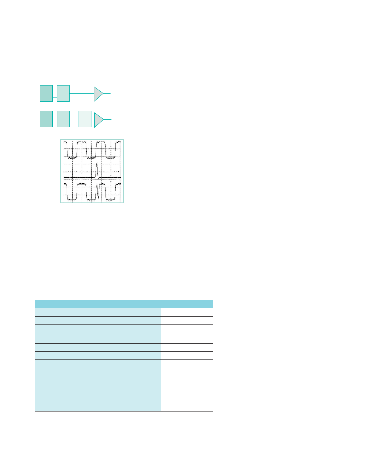
Glitch-free timing changes
Timing values can now be swept without
the danger of misleading pulses or
dropouts that could cause measurement
errors. (Applies to continuous mode,
values < 100 ms, consecutive values
between 0.5 and twice the previous value
on the 81101A, 81104A, 81110A).
Reliable measurements
All models provide clean, accurate pulses
with excellent repeatability, thus contributing to measurement integrity.
The Agilent 81110A features self-calibration
for more accuracy. It also offers a choice
of output modules. The Agilent 81111A
165 MHz 10 V module with variable transitions.
Along with the Agilent 81112A 330 MHz
3.8 V module, which has differential outputs and two selectable transition times.
The Agilent 81130A offers a choice of
output modules: the Agilent 81131A
400 MHz, 3.8 V module and the Agilent
81132A 660 MHz, 2.5 V module which has
complementary outputs.
Easy-to-use
Features such as the clear graphical
display, autoset, help, store/recall, preset
TTL/ECL levels, selectable units (such as
current/voltage, width/duty-cycle), and
load compensation ensure a high level of
convenience.
Stimulate the device’s
environment
Today’s devices can require very complex
stimuli. To meet this, the Agilent 81130A
can sequence and loop its memory for
very deep patterns. RZ (return-to-zero),
NRZ (non-return-to- zero) and R1 (returnto-one) formats are available. Digital
channel addition allows the generation
of signals with two different pulse widths
and delays or of data rates up to
1.32 Gbit/s in one single channel.
Frequency range
The Agilent 81130A is designed and
recommended for an operation in the
frequency range of 170 kHz to 400/
660 MHz. However it can be operated in
the extended range down to 1 kHz.
Agilent 81100 - Family of Pulse Pattern Generators
Mainframes 81101A 81104A 81110A 81110A 81130A 81130A
Channel model 81101A 81105A 81111A 81112A 81131A 81132A
# of channels 1 1 or 2 1 or 2 1 or 2 1 or 2 1 or 2
Frequency range 1 mHz - 50 MHz 1 mHz - 80 MHz 1 mHz - 165 MHz 1 mHz - 330 MHz 1 kHz - 400 MHz 1 kHz - 660 MHz
Variable delay range 20 ns - 999.5 s 12.5 ns - 999.5 s 6.06 ns - 999.5 s 1.515 - 999.5 2.5 ns - 1 ms 1.5 ns - 1 ms
Period RMS - jitter 0.00 s - 999.5 s 0.00 s - 999.5 s 0.00 ns - 999.5 s 0.00 ns - 999.5 s 0.00 ns to 3.00 µs 0.00 ns to 3.00 µs
Width range 10 ns to 9.995 s 6.25 ns - 9.995 s 3.03 ns - 999.5 s 1.515 ns - 999.5 s
Amplitude range 100 mV - 20.0 V
Transition time
range (10/90)
Dropout and glitch
free timing change
Source impedance 50 Ω or 1 kΩ 50 Ω or 1 kΩ 50 Ω or 1 kΩ 50 Ω 50 Ω 50 Ω
5.00 ns - 200 ms 3.00 ns - 200 ms 2.00 ns - 200 ms
Yes Yes Yes Yes No No
1
100 mV - 20.0 V
1
100 mV - 20.0 V
1
100 mV to 3.8 V 100 mV to 3.8 V 100 mV - 2.5 V
800 ps or 1.6 ns
selectable
1.25 ns -
(period-1.25 ns)
800 ps or 1.6 ns
selectable
1. Depends on selected impedance (all other values for 50 Ω source impedance into 50 Ω load).
2. 0.001% +15 ps with internal PLL as clock source.
3. Also avalable as VXI pulse pattern generators E8311A and E8312A.
750 ps (period - 750 ps)
500 ps typ.
fixed
2
Data Sheet 81100 Family of Pulse Pattern Generators
Page 3

81101A Specifications
Timing Characteristics
Measured at 50% amplitude at fastest transitions in continuous mode and 50 Ω source impedance.
Mainframe Agilent 81101A
Frequency range 1 mHz to 50 MHz
Timing resolution 3.5 digits, 5 ps best case
Period RMS jitter
• With PLL
• With VCO
Period range
• Accuracy with PLL /VCO
Width range
Accuracy
RMS jitter
• Additional variable delay range
• Accuracy
RMS jitter
• Double pulse delay range
Accuracy ±5% ± 500 ps
Transition time range (10/90) 5 ns to 200 ms variable
Accuracy ±10% ±200 ps
Linearity 3% typ. for transitions > 100 ns
2
0.001% + 15 ps
0.01% + 15 ps
20 ns to 999.5 s
± 0.01% (±5%) (similar to RMS jitter)
10.0 ns to (period - 10.0 ns)
±5% ±250 ps
0.01% + 15 ps
0 ns to (period -20 ns)
±5% ±1 ns
0.01% + 15 ps
(width + 10.0 ns) to (period- width - 10.0 ns)
1
1. Changing of amplitude may add 0.5 ns.
2. Width accuracy specification is valid up to 5.5 Vpp amplitude. Above this amplitude, the width
will typically increase up to 300 ps.
Burst Count: 2 to 65536 (single or double
pulses).
Transition times: These can be entered
as leading/trailing edge or % of width.
Leading and trailing edges are indepen-
Delay: Delay, phase or % of period.
dent within one of the following over-
lapping segments (1:20 ratio):
Double pulse delay: Double pulse and
delay are mutually exclusive.
• 5 ns - 20 ns
• 10 ns - 200 ns
Duty cycle: Set between 0.1% and 95%
(subject to width limits. 99.9% with
overprogramming).
• 100 ns - 2 µs
• 1µs - 20 µs
• 10 µs - 200 µs
• 100 µs - 2 ms
• 1 ms - 20 ms
• 10 ms - 200 ms
Repeatability: Is typically four times better
than accuracy
Output timing fidelity: Period, delay and
width are continuously variable without
any output glitches or dropouts.
Data Sheet 81100 Family of Pulse Pattern Generators
3
Page 4

Level/Pulse Performance Characteristics
Level specifications are valid after a 30 ns typical settling time.
Agilent 81101A
Amplitude 50 Ω into 50 Ω
1 kΩ into 50 Ω
Level window 50 Ω into 50 Ω
1 kΩ into 50 Ω
Accuracy 50 Ω into 50 Ω
1 kΩ into 50 Ω
Resolution 50 Ω into 50 Ω
1 kΩ into 50 Ω
Output connectors BNC single-ended
100 mVpp to 10.0 V
200 mVpp to 20.0 V
-10.0 V to +10.0 V
-20.0 V to +20.0 V
± (3% + 75 mV)
± (3% + 150 mV)
10 mV
20 mV
Load compensation: The actual load
value can be entered (for loads ≠ 50 Ω)
pp
pp
to display actual output values.
On/off: Relays connect/disconnect
output (HiZ).
1
Normal/complement: Selectable.
Limit: Programmable high and low levels
can be limited to protect the deviceunder-test.
Source impedance Selectable 50 Ω or 1 kΩ
Accuracy Typ. ± 1%
Max. external voltage ± 24 V
Short circuit current ± 400 mA max.
Base line noise 10 mV RMS typ.
Overshoot/preshoot/
ringing
± 5% of amplitude ± 20 mV
1. In ±19 V level window
Trigger modes
Continuous: Continuous pulses, double
pulses or bursts (single or double pulses).
Inputs and outputs
Clock input/PLL reference and external
input: One input (BNC connector at rear
panel) is used for clock input or alterna-
External triggered: Each active input
tively for the PLL.
transition (rising, falling or both) generates
a single or double pulse or burst.
PLL reference: The internal PLL is locked
to an external 5 MHz or 10 MHz reference
External gated: The active input level (high
frequency.
or low) enables pulses, double pulses or
bursts. The last single/double pulse or
burst is always completed.
External width: The pulse shape can be
recovered whilst the period and width of
Clock input: The output period is
determined by the signal at CLK input.
Ext. input: Used for trigger, gate or
external width.
an external input signal are maintained.
Levels and transitions can be set.
Level parameters: Can be entered as volt-
age or current, as high and low level, or as
Manual: Simulates an external input
offset and amplitude.
signal.
Input impedance: 50 Ω/10 kΩ
selectable.
Threshold: -10 V to +10 V.
Max. input voltage: ±15 Vpp.
Sensitivity: 300 mVpp typical.
Input transitions: < 100 ns.
Frequency: Dc to 50 MHz.
Minimum pulse width: 10 ns
Strobe output and trigger output trigger
format: One pulse per period with 50%
duty cycle typical.
External mode: 9 ns typ.
Level: TTL or ECL selectable.
Output impedance: 50 Ω typical.
Max. external voltage: -2 V/+7 V.
Transition times: 1.0 ns typical for TTL,
600 ps typical for ECL.
Internal triggered: Internal PLL replaces
an external trigger source.
4
Data Sheet 81100 Family of Pulse Pattern Generators
Typical delay times Agilent 81101A
Instrument mode From To Typ. value
External width Ext. input Strobe/trigger out
All other modes Ext. input/clk input
Strobe/trigger out
Output 1/output 2
Strobe/trigger out
Output 1/output 2
Output 1/output 2
8.5 ns
22.5 ns
12.0 ns
29 ns
17 ns
Page 5

81104A and 81110A Specifications
Timing characteristics
Measured at 50% amplitude at fastest transitions in continuous mode and 50 Ω source impedance.
Mainframe output module Agilent 81104A
Agilent 81105A
Frequency range
• From 1 KΩ
Timing resolution 3.5 digits, 5 ps best case 3.5 digits, 5 ps best case 3.5 digits, 5 ps best case
Period range 12.5 ns to 999.5 s 12.5 ns to 999.5 s 12.5 ns to 999.5 s
Period RMS jitter
• With PLL
• With VCO
Accuracy
• With PLL
• With VCO
Width range 6.25 ns to (period 6.25 ns) 3.03 ns to (period - 3.03 ns) 1.515 ns to (period - 1.515 ns)
Accuracy ± 5% ± 250 ps ± 0.5% ± 250 ps typ.
Jitter (RMS) 0.01% +15 ps 0.01% +15 ps 0.01% +15 ps
Add. variable delay range 0 ns to (period -12.5) 0 ns to (period -3.03 ns) 0 ns to (period -3.03 ns)
Accuracy ± 5% ± 0.5 ns ± 0.5% ± 0.5 ns typ. ± 3%
Jitter (RMS) 0.01% +15 ps
Double pulse delay range
Min period
Accuracy ± 5% ± 250 ps ± 0.5% ± 150 ps typ. ± 3%
Transition time range (10/90)
Minimum
(with overprogramming)
Accuracy ± 10% ± 200 ps typ.
Linearity 3% typ. For transitions > 100 ns 3% typ. for transitions > 100 ns N/A
1 mHz to 80 MHz
Up to 50 MHz typ.
0.001% + 15 ps
0.01% + 15 ps
0.001% +15 ps
± 0.01% (± 5%)
12.5 ns to (period - width - 6.25 ns)
25 ns (40 MHz) typ.
3 ns to 200 ms
variable
≤ 3 ns
5 ns typ. For 1 KW
± 10% ± 400 ps
Agilent 81110A
Agilent 81111A
1 mHz to 165 MHz
Up to 60 Mhz typ.
0.001% + 15 ps
0.01% + 15 ps
± 0.01%
(± 0.5% typ. after self-cal.,
± 3% without self-cal.)
After self-cal. ±3% ± 250 ps
± 0.5 ns after self-cal.
6.06 ns to (period -width - 3.03 ns)
12.2 ns (82 MHz) typ.
± 150 ps after self-cal.
2 ns to 200 ms variable
≤ 2ns/1.4 ns typ. For ELC levels
(20/80) Source impeded
± 10% ± 200 ps typ.
± 10% ± 400 ps
Agilent 81110A
Agilent 81112A
1 mHz to 330 MHz
N/A
0.001% + 15 ps
0.01% + 15 ps
± 0.01%
(± 0.5% typ. After self-cal.,
± 3% without self-cal.)
± 0.5% ± 250 ps typ.
After self-cal. ±3% ± 250 ps
± 0.5% ± 0.5 ns typ. ± 3%
± 0.5 ns after self-cal.
3.03 ns to (period - width - 1.5)
6.06 ns (165 MHz) typ.
± 0.5% ± 150 ps typ. ± 3%
± 150 ps after self-cal.
± 0.5% ± 150 ps typ. ± 3%
± 150 ps after self-cal.
0.8 ns or 1.6 ns selectable
≤ 600 ps for Vpp ≤ 1 V
450 ps typ. for ELC levels (20/80)
≤ 900 ps for Vpp > 1 V
± 10% ± 200 ps typ.
± 10% ± 400 ps
1. Source impedance is selectable from 50 Ω to 1 KΩ for the Agilent 81111A.
2. Changing of amplitude may add 0.5 ns.
Transition times: leading/ trailing edge
or % of width. Leading and trailing edges
Burst count: 2 to 65536 (single or double
pulses).
are independent Agilent 81111A/Agilent
81105A) within one of the following
overlapping segments (1:20 ratio):
Delay: Delay, phase or % of period.
• 2 ns (3 ns) - 20 ns
Double pulse and delay: Mutually exclusive.
Duty cycle: Set between 0.1% and 95%
(subject to width limits. 99.9% with overprogramming).
• 10 ns - 200 ns
• 100 ns - 2 ms
• 1µs - 20 µs
• 10 µs - 200 µs
• 100 µs - 2 ms
Repeatability: Is typ. four times better than
accuracy.
• 1 ms - 20 ms
• 10 ms - 200 ms
Data Sheet 81100 Family of Pulse Pattern Generators
Output timing fidelity: Period, delay and
width are continuously variable without
any output glitches or dropouts.
Overprogramming: All parameters of the
Agilent 81110A, except transitions, can
be set to whatever the 330 MHz timing
system will allow. This applies also when
the Agilent 81111A (165 MHz) output
module is used.
5
Page 6

Level/Pulse Performance Characteristics
Level specifications are valid after a 5 ns (Agilent 81112A) or 30 ns (Agilent 81111A/Agilent 81105A) typical settling time.
Mainframe Agilent 81101A
Agilent 81105A
Amplitude 50 Ω into 50 Ω 100 mVpp to 10.0 V
Level window 50 Ω into 50 Ω
1 kΩ into 50 Ω
Accuracy 50 Ω into 50 Ω
1 kΩ into 50 Ω
Resolution 50 Ω into 50 Ω
1 kΩ into 50 Ω
Output connectors BNC single-ended BNC single-ended BNC differential
Source impedance Selectable 50 Ω or 1 kΩ Selectable 50 Ω or 1 kΩ 50 Ω only
Accuracy Typ. ± 1% Typ. ± 1% Typ. ± 1%
Max. external voltage ± 24 V ± 24 V -2.2 V to +5.5 V
Short circuit current ±400 mA max.
Dynamic crosstalk < 0.1% typ. < 0.1% typ. < 0.1% typ.
Base line noise 10 mV RMS typ. 4 mV RMS typ. 10 mV RMS typ. 4 mV RMS typ. 10 mV RMS typ. 4 mV RMS typ.
Overshoot/preshoot/ringing ± 5% of amplitude ± 20 mV ± 5% of amplitude ± 20 mV ± 5% of amplitude ± 50 mV
-10.0 V to +10.0 V
-20.0 V to +20.0 V
± (3% + 75 mV)
± (3% + 150 mV
10 mV
20 mV
(doubles for channel addition)
pp
1
Agilent 81110A
Agilent 81111A
100 mVpp to 10.0 V
-10.0 V to +10.0 V
-20.0 V to +20.0 V
± (1% + 50 mV)
± (1% + 100 mV)
10 mV
20 mV
±400 mA max.
(doubles for channel addition)
pp
1
Agilent 81110A
Agilent 81112A
100 mVpp to 3.8 V
- 2.0 V to 3.8 V
N/A
± (2% + 50 mV)
N/A
10 mV
N/A
-84 mA to + 152 mA
pp
1. In ± 19 V level window.
Level parameters: voltage or current, high
or low level, offset or amplitude.
On/off: relays connect/ disconnect output
(HiZ).
Load compensation: the actual load value
can be entered (forloads ≠ 50 Ω) to display
actual output values. (Applies to the
Agilent 81105A and Agilent 81111A only).
Normal/complement: selectable.
Limit: programmable high and low levels
can be limited to protect the device-undertest.
Channel Addition (with Agilent 81105A or Agilent 81111A output channels)
If the instrument is equipped with 2 output modules, channel 2 can be added to channel 1 internally. In this case the second output is
disabled. The additional fixed delay on the second channel is typ. 2.5 ns. The following parameters differ from the above specifications if
two output modules (Agilent 81105A/Agilent 81111A) are added.
Mainframe Agilent 81104A with two
Agilent 81105A output modules
Amplitude 50 Ω into 50 Ω
Source impedance Selectable from 50 Ω or 1 kΩ Selectable from 50 Ω or 1 kΩ
Level window 50 Ω into 50 Ω
Max. frequency 50 Ω into 50 Ω
Min. transitions 50 Ω into 50 Ω
6
1 kΩ into 50 Ω
1 kΩ into 50 Ω
1 kΩ into 50 Ω
1 kΩ into 50 Ω
Data Sheet 81100 Family of Pulse Pattern Generators
100 mVpp tp 20.0 Vpp
200 mVpp to 20.0 Vpp
-20.0 V +20.0 V
-20.0 V to +20.0 V
60 MHz typ.
15 MHz typ.
2 ns typ. (channel one) 5 ns typ. (channel two)
20 ns typ. both channels
Agilent 81110A with two
Agilent 81111A output modules
100 mVpp tp 20.0 Vpp
200 mVpp to 20.0 Vpp
-20.0 V +20.0 V
-20.0 V to +20.0 V
60 MHz typ.
15 MHz typ.
2 ns typ. (channel one) 5 ns typ. (channel two)
20 ns typ. both channels
Page 7

Pattern mode
Pattern length: 16 kbit/channel and
strobe output.
Output format: RZ (return to zero), NRZ
(non-return to zero), DNRZ (delayed
non-return to zero).
Random pattern:
PRBS 2 ^ (n - 1) n = 7,8,...,14.
Trigger modes
Continuous: Continuous pulses, double
pulses, bursts (single or double pulses)
or patterns.
Inputs and Outputs
Clock input/PLL reference and
external input
PLL reference: (BNC connector at rear
panel). The internal PLL is locked to an
external 5 MHz or 10 MHz reference
frequency.
Clock input: (BNC connector at rear
panel). The output period is determined
by the signal at CLK input.
Ext. input: Used for trigger, gate or
external width.
Input impedance: 50 Ω/10 kΩ selectable.
Strobe output and trigger output
Strobe output: User-defined, 16 kbit
pattern (NRZ) when in pattern mode.
Trigger format: One pulse per period with
50% duty cycle typical. External mode:
1.5 ns typ. for Agilent 81110A. 5.9 ns typ.
for Agilent 81104A.
Level: TTL or ECL selectable.
Output impedance: 50 Ω typical.
Max. external voltage: - 2 V/+7 V.
Transition times: 1.0 ns typical for TTL,
600 ps typical for ECL.
External triggered: Each active input
transition (rising, falling or both)
generates a single or double pulse,
burst or pattern.
External gated: The active input level
(high or low) enables pulses, double
pulses, bursts or patterns. The last
single/double pulse, burst or pattern
is always completed.
External width: The pulse shape can be
recovered. Period and width of an external
input signal is maintained. Delay, levels
and transitions can be set.
Manual: Simulates an external input
signal.
Internal triggered: Internal PLL replaces
an external trigger source. Pulses, double
pulses, bursts or patterns can be set.
Typical delay (Agilent 81110A with Agilent 81111A output module)
Threshold: - 10 V to + 10 V.
Max. input voltage: ± 15 Vpp.
Sensitivity: ≤ 300 mVpp typical.
Transitions: < 100 ns.
Frequency: dc to max. frequency
of output module.
Min. pulse width: 1.5 ns (as width of
output module in external width mode).
1
Instrument mode From To Typ. value
External width Ext. input Strobe/trigger out
Output 1/output 2
All other modes Ext. input/clk input Strobe/trigger out
Output 1/output 2
Strobe/trigger out Output 1/output 2 14.0 ns
1. Subtract 4 ns from the typ. delay value when referring to OUTPUT 1 / 2 for the Agilent 81112A output module and add 1 ns when referring to
OUTPUT 1 / 2 for the Agilent 81104A with the Agilent 81105A output module.
8.5 ns
19.5 ns
12.0 ns
26.0 ns
Data Sheet 81100 Family of Pulse Pattern Generators
7
Page 8

81130A Specifications
Timing characteristics
Measured at 50% amplitude at fastest transitions in continuous mode and 50 Ω source impedance. The Agilent 81130A is designed and
recommended for an operation in the frequency range of 170 kHz to 400/660 MHz. However it can be operated in the extended range
down to 1 kHz. Changes in specifications below 170 kHz are marked.
Mainframe
Output module
Frequency range 170 kHz (1 kHz) to 400 MHz 170 kHz (1 kHz) to 660 MHz
Frequency resolution 4 digits, (2 ps best case)
Period range 2.5 ns to 5.9 µs 1.50 ns to 5.9 µs
Accuracy ± 100 ppm
RMS jitter (int ref, int clk) 0.001% + 15 ps
Width range 1.25 ns to period - 1.25 ns) 750 ps to period - 750 ps
Width resolution 4 digits ( 2 ps best case)
Width accuracy ± (100 ppm + 200 ps)
Width jitter 0.001% + 15 ps 0.001% + 15 ps
Add, variable delay range 0 to 3.00 µs independent of period
Delay resolution 4 digits (2 ps best case )
Delay accuracy ± (0.01% + 100 ps) relative to zero delay
Delay jitter 0.001% + 15 ps 0.001% + 15 ps
Fixed delay
• Clk in to out
• Ext. in to out
Transition time range (10/90) 800 ps or 1600 ps Fixed
Minimum transition (10/90) ≤ 600 ps for Vpp ≤ 1 V
At ELC levels (20/80) 450 ps typ. < 500 ps (400 ps typ.)
Deskew range ± 25 ns ± 25 ns
Agilent 81130A
Agilent 81131A
(f < 170 kHz: 2.5 ns to 1 ms)
(f < 170 kHz: 0.05% of period)
(f < 170 kHz: 0.06% of period)
( > 3 µs: one to 1 period)
(f < 170 kHz: ± 0.05% of period)
(f < 170 kHz: ± 0.035% of period)
53 ns
54 ns + 0 to 1 period
≤ 900 ps for Vpp ≤ 1 V
1
Agilent 81130A
Agilent 81132A
(f < 170 kHz: 1.5 ns to 1.0 ms)
4 digits ( 2 ps best case)
(f < 170 kHz: 0.05% of period)
± (100 ppm + 200 ps)
(f < 170 kHz: 0.06% of period)
0 to 3.00 µs independent of period
( > 3 µs: one to 1 period)
4 digits (2 ps best case )
(f < 170 kHz: ± 0.05% of period)
± (0.01% + 100 ps) relative to zero delay
(f < 170 kHz: ± 0.035% of period)
53 ns
54 ns + 0 to 1 period
500 ps typ.
1
1. The uncertainty of 1 period can be eliminated if an external clock and the following setup and hold times are upheld. setup time: 0.3 ns to 4.3 ns;
hold time: -2.8 ns to 4.0 ns.
Burst count: 2 to 65504.
Delay: Delay, phase or % of period.
Duty cycle: Set between 0.1% and 99,9% (subject to width limits).
Repeatability: Is typ. four times better than accuracy.
8
Data Sheet 81100 Family of Pulse Pattern Generators
Page 9

Level/Pulse Performance Characteristics
Level specifications are valid after a 30 ns typical settling time (50 Ω into 50 Ω terminated to ground).
Mainframe
Output module
Amplitude 0.10 Vpp to 3.80 Vpp 0.10 Vpp to 2.50 Vpp
Level
• Window -2.00 V to +3.80 V -2 .00 V to +3.00 V
• Accuracy ± (5% +150 mV) ± (5% +150 mV)
• Resolution 3 digits (10 mV best case) 3 digits (10 mV best case)
Output impedance 50 Ω ± 1% typ. 50 Ω ± 5% typ.
Max. external voltage -2.2 to +5.5V -2.0 to +4.0 V
Short circuit current -80 mA to +152 mA. -80 mA to +120 mA
Baseline noise 4 mV RMS typ. 8 mV RMS typ.
Overshoot/preshoot/ringing ± (5% + 50 mV) of amplitude typ. ± (5% + 100 mV) of amplitude typ.
Level parameters: Voltage or current, high
and low level, or offset and amplitude.
Pattern and sequencing
Pattern length: 65504 bit/channel. If
PRBS is used: (65503-RBLength).
Pattern formats: NRZ (non-return-to-zero),
DNRZ (delayed non-return-to-zero), RZ
(return-to-zero) and R1 (return-to-one) can
be selected (see Figure 1).
On/off: Relays connect/disconnect
81130A
81131A (400 MHz)
Sequencing: A sequence is a succession
of segments. One outer loop running once
or continuous, and one nested loop can be
applied. The nested loop can be set from
1 to 2 ^ 20 repetitions.
Segment: The memory can be divided into
maximal 4 segments.
Segment length resolution: This is the
resolution for which the segment can be
set dependent on the maximum data rate.
See Table 1.
81130A
81132 A (660 MHz)
Limit: Programmable high and low levels
can be limited to protect the device-undertest.
Segment types: Pattern, PRBS, high
and low segments ( “0” or “1” levels
segments selectable).
Note: If one channel is set to PRBS the
other channel can only be high or low
segments, or PRBS type.
Random pattern: PRBS 2 ^ n - 1,
n = 7,8,...,15 (CCITT 0.151).
output (HiZ).
Output pattern formats
Non-return-to-zero
Delayed non-return-to-zero
Return-to-zero
Return-to-one
1
NRZ
DNRZ
RZ
R1
1 bit period
121
Width is a multiple
of clock periods.
The signal can be
delayed as required.
Width and delay can
be set as required.
Width and delay can
be set as required.
Data Sheet 81100 Family of Pulse Pattern Generators
Segment length resolution trade-offs
Required segment
length resolution
1 bit 41.67
2 bits 83.88
4 bits 166.67
8 bits 333.33
16 bits 660
1. The minimum length in the first segment of a nested
loop is two times that of the segment length resolution.
Maximum data
1
rate, Mbits/s
9
Page 10
Digital channel addition
Channel 1 can be logically combined with
channel 2 (XOR) as shown in Figure 2. The
source impedance remains 50 Ω. Output 2
is still available in this case.
Channel 1
Delay,
Data
Data
width
Channel 2
Delay,
width
XOR
Channel 1
Channel 1 +
Channel 2
Trigger modes
Continuous: Continuous pulses, bursts or
patterns.
External started: Each active input transition (rising, falling edge) generates pulses,
bursts or patterns.
External gated: The active input level
(high or low) enables pulses, bursts or
patterns. On an external gate signal the
output is immediately stopped, that means
the last cycle will not be completed.
Manual: Simulates an external input
signal with push of a front panel button.
External clock: The output period is
determined by the signal at clock input.
Clock input frequency: 170 kHz to 660 MHz
(at 50% ±10% duty cycle).
Delay from input trigger output: 21 ns.
Delay from input to output: 53 ns.
Threshold: ac coupled. Only valid for external
input.
External input: Used for external started or
gated.
Input frequency: DC to 330MHz.
Channel 1
Inputs and outputs
Clock input/PLL reference and
Channel 2
Channel 1 +
Channel 2
external input
Connectors: SMA (f) 3.5 mm
Input impedance: 50 Ω
Termination voltage: -2.10 V to 3.30 V
Input sensitivity: < 400 mV typ.
Figure 2: Channel addition
Max. input voltage: -3 V to + 6 V
Input transitions: < 20 ns
Only valid for clock input/PLL reference
One input is used for clock input or for the
PLL reference alternatively.
Reference: The internal PLL is locked to
the 1,2,5 or 10 MHz. The output frequency
of the instrument must be larger than the
clock input/PLL reference frequency.
Programming times: (measured at display off)
ASCII command Typical execution time
Width, delay, transition times 40 ms to 70 ms
Period within one range 1 100 ms to 260 ms
Period between different ranges:
• In pulse/burst mode
• in pattern mode
Levels 43 ms
Trigger modes < 75 ms
Input parameters 28 ms
Save setting 200 ms
Recall setting:
a) In pulse/burst mode
b) In pattern mode with data and PRBS (depends on setting)
65504 bit pattern transfer 1.25 s
Pattern and sequencing (depends on setting) 190 ms to 5.1 s
1
140 ms to 300 ms
100 ms to 5.05 s
515 ms to 800 ms
1.15 s to 5.5 s
Delay from external input to trigger output:
22ns + 0 to 1 period.
Delay from external input to output:
54 ns + 0 to 1 period.
Threshold: -1.4 V to +3.7 V.
Trigger output
Trigger format: One pulse per period with
50% duty cycle typical. In pattern mode the
trigger pulse can be set to mark the start of
any segment.
Output impedance: 50 Ω typical.
Level: TTL/ETTL (for frequency < 180 MHz),
1 V to GND, ECL 50 Ω to GND/-2 V, PECL
50 Ω to + 3 V.
Max. external voltage: -2 V/+3 V.
Transition times: 1.0 ns typical for TTL,
600 ps typical for ECL.
Delay from external input to trigger output:
32 ns typical.
1. Range depends on segment length resolution, see previous table.
10
Data Sheet 81100 Family of Pulse Pattern Generators
Page 11

Common Specifications
General
Inputs and outputs
User interface
Overprogramming: All parameters can
be overprogrammed (exceeding specifications) to fully exploit the hardware limits.
Setting check: Warning messages
indicate potentially conflicting parameters
due to inaccuracy. Error messages indicate
conflicting parameters.
Help key: Displays a context-sensitive
message.
Autoset key: Resolves all timing conflicts.
Non-volatile memory: Current setting is
saved on power-down. Up to nine user
settings and one fixed default setting can
be stored in the instrument.
Memory card: 99 settings can be stored
on a 1 MB PCMCIA card (MS-DOS®).
Remote control: Operates according
to IEEE standard 488.2, 1987 and SCPI
1992.0.
Function code: SH1, AH1, T6, L4, SR1,
RL1, PP0, DC1, DT1, C0.
Programming times: All checks and
display off.
ASCII command Typ. exec. time
One parameter or
mode
Recall setting 250 ms typ.
16 k pattern transfer 600 ms typ.
30 ms typ.
Operating temperature: 0 °C to +55 °C.
Storage temperature: -40 °C to +70 °C.
Humidity: 95% r.h. up to 40 °C ambient
temperature.
EMC: conforms to EN50082-1, EN 55011,
Class A.
Noise emission: 5.7 bel typical.
Battery: Lithium CR2477-N.
Safety: IEC1010, CSA1010.
Power requirements:
100 - 240 Vac, ± 10%, 50 - 60 Hz
100 - 120 Vac, ± 10%, 400 Hz.
Power consumption: 300 VA max.
Max. dimensions: (H * W * D):
89 mm * 426 mm * 521 mm.
Weight: 9.2 kg net, 13.8 kg shipping.
Recalibration period:
Three years recommended.
Complementary products - pulse
pattern generator and oscilloscopes
(real time or sampling)
• DSO 80804B/80604B
• DSO 80404B
• DSO 80304B
• D/MSO 6100/8104A
• D/MSO 6050/8064A
• D/MSO6030
• D/MSO 601x
• DSO 3000
Clock input/PLL reference and external
input.
Connectors: SMA (f) 3.5 mm.
Input impedance: 50 Ω.
Termination voltage: -2.10 V to 3.30 V.
Input sensitivity: < 400 mV typ.
Max. input voltage: -3 V to + 6 V.
Input transitions: < 20 ns.
Only valid for clock input/PLL reference.
One input is used for clock input or for
the PLL reference alternatively.
Reference: The internal PLL is locked to
the 1, 2, 5 or 10 MHz.
External clock: The output period is
determined by the signal at clock input.
Clock input frequency: 170 kHz to
660 MHz (at 50% ±10% duty cycle).
Delay from input trigger output: 21 ns.
Delay from input to output: 53 ns.
Threshold: ac coupled. Only valid for
external input.
External input: Used for external started
or gated.
Input frequency: DC to 330 MHz.
Delay from external input to trigger
output: 22 ns + 0 to 1 period.
Delay from external input to output:
54 ns + 0 to 1 period.
Specifications
Specifications describe the instrument’s warranted performance. Non-warranted values are described as typical. All specifications apply
after a 30 minute warm-up phase with 50 Ω source/load resistance. All specifications are valid from 0 °C to 55 °C ambient temperature.
Data Sheet 81100 Family of Pulse Pattern Generators
11
Page 12

Ordering Information - 81100 Family
The minimum configuration for a working instrument consists of a mainframe and one output module. The second output module can
be added later. Output modules can be exchanged and retrofitted by the user. The Reference Guide (811xx-91021) is supplied with each
mainframe for all configurations. A memory card is not included.
Each Agilent 81101A mainframe includes
one output channel (in comparison to the
other models of the Agilent 81100 family).
The output module of the 81101A does not
need to be ordered separately.
Agilent 81101A
50 MHz one channel pulse generator, 10 V
Quick start guide language options
Opt OBI Engish Guide
(811xx-91021)
Opt ABF French Guide
(81101-91210)
Opt ABJ Japanese Guide
(81101-91510)
Opt AB0 Taiwan Chinese Guide
(81101-91610)
Opt AB1 Korean Guide
(81101-91710)
Opt AB2 Chinese Guide
(81101-91810)
Additional documentation options
Opt 0BW Service Manual
(81101-91021)
All options are orderable with the
mainframes.
Accessories
Opt UN2 Rear panel connectors (instead
of front panel)
Opt 1CP Rack mount and handle kit
(5063-9219)
Opt 1CN Handle kit (5063-9226)
Opt 1CM Rack mount kit (5063-9212)
Opt 1CR Rack slide kit (1494-0059)
Opt UFJ 1 MB SRAM memory card
(0950-3380)
Opt UK6 Commercial cal. certificate with
test data
Agilent 81104A
80 MHz pulse/pattern generator
mainframe
Output module:
Agilent 81105A 80 MHz, 10 V
Agilent 81110A
330/165 MHz pulse/pattern generator
mainframe
Output modules:
Agilent 81111A 165 MHz, 10 V
Agilent 81112A 330 MHz, 3.8 V
Note: Only use output modules of the
same module number. A combination of
the Agilent 81111A and Agilent 81112A in
one Agilent 81110A is not possible.
Quick start guide language options
Opt OBI Engish Guide
(811xx-91021)
Opt ABF French Guide
(81110-91210)
Opt ABJ Japanese Guide
(81110-91510)
Opt AB0 Taiwan Chinese Guide
(81110-91610)
Opt AB1 Korean Guide
(81110-91710)
Opt AB2 Chinese Guide
(81110-91810)
Additional documentation options
Opt 0BW Service Manual
(81110-91021)
Agilent 81130A
400/660 MHz pulse/data generator
mainframe
Output modules:
Agilent 81131A 400 MHz, 3.8 V
Agilent 81132A 660 MHz, 2.4 V
Note: Only use output modules of the
same module number. A combination of
the Agilent 81131A and Agilent 81132A in
one Agilent 81130A is not possible.
Quick start guide language options
Opt OBI Engish Guide
(811xx-91021)
Opt ABF French Guide
(81130-91220)
Opt ABJ Japanese Guide
(81130-91520)
Opt AB0 Taiwan Chinese Guide
(81130-91620)
Opt AB1 Korean Guide
(81130-91720)
Opt AB2 Chinese Guide
(81130-91820)
Additional documentation options
Opt 0BW Service Manual
(81130-91021)
Opt 0B1 English Quick Start
Guide (includes English
Referemce Guide)
Opt ABJ Japanese Quick Start
Guide (includes English
Referecnce Guide)
Opt 0B0 Does not include any
Quick Start Guide
(includes English
Reference Guide)
Data Sheet 81100 Family of Pulse Pattern Generators12
Page 13
Related Agilent literature Pub. no.
Agilent Family of Pulse/
Pattern Generators,
Brochure
Radar Distance test to
airborne planes
Application Note
The Dual Clock Gbit Chip
test Application Note
For more information, please visit us at
www.agilent.com/find/pulse_generator
For the latest version of this document,
please visit our website at:
www.agilent.com/find/pulse
and go to the key library information
area or insert the publication number
(5980-1215E) into the search engine.
5980-0489E
5968-5843E
5968-5844E
Agilent Email Updates
www.agilent.com/find/emailupdates
Get the latest information on the
products and applications you select.
www.lxistandard.org
LXI is the LAN-based successor to
GPIB, providing faster, more efficient
connectivity. Agilent is a founding
member of the LXI consortium.
Agilent Channel Partners
www. agilent.com/find/channelpartners
Get the best of both worlds: Agilent’s
measurement expertise and product
breadth, combined with channel
partner convenience.
Remove all doubt
Our repair and calibration services
will get your equipment back to
you, performing like new, when
promised. You will get full value out
of your Agilent equipment throughout its lifetime. Your equipment
will be serviced by Agilent-trained
technicians using the latest factory
calibration procedures, automated
repair diagnostics and genuine parts. You
will always have the utmost confidence
in your measurements. For information
regarding self maintenance of this
product, please contact your Agilent
office.
Agilent offers a wide range of additional
expert test and measurement services
for your equipment, including initial
start-up assistance, onsite education
and training, as well as design, system
integration, and project management.
For more information on repair and
calibration services, go to:
www.agilent.com/find/removealldoubt
www.agilent.com
www.agilent.com/find/pulse
For more information on Agilent
Technologies’ products, applications or
services, please contact your local Agilent
office. The complete list is available at:
www.agilent.com/find/contactus
Americas
Canada (877) 894 4414
Latin America 305 269 7500
United States (800) 829 4444
Asia Pacific
Australia 1 800 629 485
China 800 810 0189
Hong Kong 800 938 693
India 1 800 112 929
Japan 0120 (421) 345
Korea 080 769 0800
Malaysia 1 800 888 848
Singapore 1 800 375 8100
Taiwan 0800 047 866
Thailand 1 800 226 008
Europe & Middle East
Austria 43 (0) 1 360 277 1571
Belgium 32 (0) 2 404 93 40
Denmark 45 70 13 15 15
Finland 358 (0) 10 855 2100
France 0825 010 700*
*0.125 €/minute
Germany 49 (0) 7031 464 6333
Ireland 1890 924 204
Israel 972-3-9288-504/544
Italy 39 02 92 60 8484
Netherlands 31 (0) 20 547 2111
Spain 34 (91) 631 3300
Sweden 0200-88 22 55
Switzerland 0800 80 53 53
United Kingdom 44 (0) 118 9276201
Other European Countries:
www.agilent.com/find/contactus
Revised: October 1, 2009
Product specifications and descriptions in
this document subject to change without
notice.
© Agilent Technologies, Inc. 2009
Printed in USA, November 24, 2009
5980-1215E
 Loading...