

Page 1

Service Manual
DiVA A85, P85 & P85/3
Amplifi ers
A85
Issue 2.0
ARCAM
Page 2

Contents List
!
Contents list
!
Circuit description
!
Service guide
!
Circuit diagrams
!
Component overlays
!
Circuit board parts list
!
General assembly parts list
Page 3

Pre-amplifier circuit description
The A85 preampli fier is a high-performanc e, DC coupled design
with microproc essor control of in put select, two in dependent tap e
loops, electronic volume control, tone bypass and electronic tone
control.
It features a discrete power supply and low-noise linear circuitry to
obtain very good distortion and noise performance, suitable for
high quality sourc e m aterial such as CD or DVD-A.
Input switching
Each of the inputs has a pair of diodes to the ±15V rails to prevent
static spikes from causing damage t o the CMOS multip lexers. In
addition, there is a simple resistor-capacitor filter with a corner
frequency of approximately 340kHz to remove any unwanted high
frequency interference from the signal. This uses high-quality
polypropylene capacitors for best performance.
Z104 and Z105 are the main input select multipl exers, which are
configured in a ‘virtual earth’ unity gain arrangement with Z115
and Z116. This arrangement is slightly lower distortion than the
‘normal’ one, at th e cost of a slightly higher nois e floor. It is an
inverting configuration, which is restored to correct polarity by the
inverting elect r onic volume control which follows.
Z115B and Z116B are integrating servos, which take out any DC
from the input signal before the following stages. The servos are 2pole, with a passive 2
the left channel) to remove broadband noise from the output of the
servo and improve speed of response.
Z100 thru Z103 are the input selectors for t he 2 tape loops . These
are normal non-inverting selectors which are buffered before being
passed on to the phono sockets.
Z109A output is decoupled by R108 which is included in the
feedback path . Local h igh freq u ency feed ba ck occu rs aroun d C108
to allow the tape loop output to be very low impedance, whilst
being stable into a capacitive load such as may be presented by a
screened in terconnect cable. This is the same for all tape outputs.
Z106 is configured as a double pole changeover switch, used to
select the tone controls. The tone controls are bypassed when not
required so that the noise and distortion can be minimised.
Tone control circuit
The tone control circuit is a non-inverting one, using a gyrated
‘bell’ filter f o r the bass and a simple shelving filter for the t r eble.
Left channel description
The input is attenuated by 6dB and biased to a volt age of +2.5V
DC by C111, R113, R112, R110, R111 and C110 . This is so the
signals fall within the 0 - 5VDC required by the digital
potentiometer Z108.
Z111B and its associated components form an active equivalent of
a series resonan t LCR circui t. This has a n impedance m inimum of
5.4k at around 80Hz with Q=0.7 The reason the bass is done as a
band-boost filter rather than a shelving filter is so that you can
boost the ‘real’ b as s wit hout c ausi ng lot s of s u b- aud i o lou dsp eak er
cone excursion which wastes power and may damage the drive
units.
nd
pole being formed by R180 and C147 (for
The digital pots Z108D and Z108A control the bass and treble
respectively. Th is is done by moving the wiper conn ected to the
frequency-sensitive impedance between the non-inverting and
inverting terminals of Z112A, effectively changing the ratio of
feedback boost and feed-forward attenuation of the circuit at the
desired frequencies, thus providing a EQ gain control that is
symmetrical on a logarithmic scale, with the use of a linear pot.
Z112B provides the 6dB of gain necessary to bring the nominal
signal level back to unity. C116 and C117 remove the 2.5VDC
offset from th e output, to preven t clunks when th e tone controls
are activated.
Z108 is controlled by a simple 3-wire serial interface from the
microprocessor. Each of th e digit al lin es has it s own groun d return
to minimise electromagnetic interference. They are connected
together only at the GND pin of the IC.
Volume control
Z107 is a VSDVC electronic volume control IC. It works, in
conjunction with an external op-amp , by varying t he feed-for ward
and feedback resi stors in an inverting gai n configuration. In th is
way, it can allow output signal swings of up to 22Vpp whilst
operating from a sin gle +5VDC power supply. Also, it allows th e
user the choice of external ci rcuitry to fine-tune the p erformance.
The gain is controlled from th e microprocessor via a 3 -wire serial
interface. The analogue supply rail is derived from the local +5V
via R185 and C156 // C157.
Z117 is the output op-amp. Its outputs a re decoupled via R186,
R187, C158 and C159 so that it has a low output impedance but
can drive cable capacitance without oscillation. R186 and R187
are included in the audio frequency feedback loop to reduce output
impedance when driving ‘difficult’ cables.
RLY100 is a mute relay which shunts the preamp output to
ground. This is to prevent thumps and squeals when the units is
powered up or down.
Power supply
The transformer winding is connected to SK300. The voltage is
rectified and smoothed by D300, D301, D306, D307 and C300,
C310. The un regulated voltage sh ould be around ±27VDC. F300
and F301 are secondary fuses, as the low power preamp winding
would not blow the primary fuses if short circuited.
The voltage regulators a re discrete compound emi tter followers. I
will describe the +15V supply as the negative is essentially an
exact mirror image.
Q300 and R300 act as a constant current source, supplying around
7mA into D310. C302 and C314 reduce ripple and broadband
noise on the zen er diode. Q3 05 and Q306 form a complementary
Darlington NPN transistor which is configured as an emitter
follower, produ cing the + 15VDC at its output. C303 is to pr ovide
bulk charge stora ge an d t o reduce t he AC out put impedanc e of th e
power supply. D302 prevents reverse bias of the supply during
power down.
Z301 is a conventional LM317 type circuit to drop the +15V rail
down to +5V for the tone and volume control circuits.
Star point SP300 explicitly connects the differently named ground
nets together at one point, to minimise hum.
Page 4

Amplifier & PSU Circuit Description
L882PB is the printed circuit board that provides the power supply
and output stage amplifiers for the A85 integrated and power
amplifiers.
Its function is to:
1. Drive the loudspeakers(!)
2. Provide an (always on) auxiliary 5VDC supply for the micro
controller and display interface
3. Receive logic signals from the micro controller to turn on
the main amp lifier supply rela y (mains) and connect either
pair of speaker output sockets
4. Send logic signals to the micro controller pertaining to the
state of the amplifiers (short circuit protection, DC offset
protection, t hermal protection)
5. Receive and demodulate RC5 remote style control codes via
the rear pan el jack and trans mit them to the micr o controller
6. Send a 12V trigger ou tput via the rea r pan el jack for con trol
of an auxiliary power amp when the unit is on
7. Receive a 12V trigger input from the rear jack (for u s e in the
power amp only version)
8. Drive a pair of headphones via attenuating resistor networks
The power amplifier is a symmetrical, class B, bipolar junction
transistor output, current-feedback design (of which more later)
with DC-coupled signal and feedback paths, featuring an active
integrating volta ge servo to control DC offsets.
It features ‘instantaneous’ safe operating area protection in
addition to sending a signal to the micro to turn off the output
relays in the even t of user or thermal ove rload. Since it i s a DCcoupled desi gn, the unit senses DC at the output and triggers the
micro to turn of f the loudspeak er relays in the even t of excessive
levels (possibly due to a faulty source component or short circuit
output transistor).
The output s tage uses Sank en specia lised ‘audio a mplifier’ pow er
bipolar Darlington transistors which are optimised for use with this
type of topology. Consequently the unit has excellent measured
performance in terms of noise, slew rate, output impedance and
distortion (harmonic and intermodulated) and is essentially load
invariant (to a first order th e measu red p erforman ce i s ind epend ent
of the load impedance).
L882 Circuit Sheet 1
The audio input to the amplifier is connected to SK102 (which
connects to the output of the preamp PCB). This signal is passed
on via SK104A which forms the preamp out connection to the
outside world.
SK104B provides the power amp input connection, with switch
SW100 selecting between pre / power and integrated modes. The
unit is wired as a preamp / power amp combination with the switch
depressed, allowing the user to insert a processor or other function
(e.g. graph ic EQ) between th e output of th e preamp and th e input
of the power amp. With the switch in the ‘out’ position the power
amp input socket is ignored and the input to the power amp is
connected internally to the output of the preamp. PL100 and
PL101 are ‘handbag’ links fitted to the power amp only version to
connect both pairs of phono sockets in parallel for daisy chaining
(as there is no preamp output on a power amp).
Relays RLY100 and RLY101 switch the two pairs of loudspeaker
output sockets and are controlled by the micro lines describes
above. Transistors TR100 and TR101 operate in ‘constant current
sink’ mode which allow relay current to be approximately constant
although the main power supply rails will vary with mains input
and load conditions. The current is around 20mA per relay.
Star point SP100 is the ground ‘mecca’ for the entire amplifier
(comprising a ll three PCBs wit hin the unit ). All of the sepa rately
named grounds are joined explicitly at this point. Different named
grounds are used to ensure that no two ‘different’ grounds share
copper, which could compromise the noise, distortion or crosstalk
performance of the amplifier.
The loudspeaker output signals are passed to socket SK106 which
connects to SK107 and onto the headphone output via the
attenuation resistors R103 thru R106.
The hierarc hy con tai ning t he oth er sheet s i s self expla na tory. E ach
of the port names shown on the top sheet connects t o the port of
the same na me on the lower sheets.
L882 Circuit Sheet 2
This sheet contains the power supplies, the rear panel jack socket
trigger circuits, the standby relay control and the ‘interface’
circuits between the output signals of the power amplifiers and the
inputs expected by the micro processor.
The mains input enters the unit at SK203, with capacitors C205
and C206 acting as conducted RF suppression. The earth
connection is passed on to the chassis (for safety reasons the
chassis metalwork remains connected to mains power earth at all
times). Switch SW200 is the voltage selector switch, allowing the
unit to be operated in 230V or 115V mains countries by switching
the dual-primary mains transformers between series and parallel
winding. Varistors VR200 and VR201 act to prevent over-voltage
surges from da maging the unit . If the user selec ts 115V opera tion
and then connec ts the unit to a 230V sup ply, the varist ors will go
to a low impedance and blow the primary fuses. Any very high
voltage line transients will also be suppressed, helping to eliminate
transformer isola tion breakdown.
Relay RLY200 switches the primary side of the mains transformer,
allowing the micro to control th e on / off status of th e amplifier. Its
contacts are snubbed by capacitors C207 and C208 (to eliminate
switching spark transients and prolong relay lifespan). The primary
windings of the toroidal mains transformer connect to SK204.
PCB mounted transformer TX200 is powered all the time that
mains is presen t on S K203 , i rres p ective of t h e on / off st at u s of the
amplifier. This is to ensure that the micro processor is always
operational and can thus control the mains switching for the main
amplifier. Secondary fuse F202 limits the current in the event of a
failure mode, as the short circuit primary current of TX200 would
be insufficient to blow the mains fuses.
Diodes D200 thru D203, C227 and IC201 provide the 5VDC
supply which powers the micro and display PCB and the relay
coils. C224 is to reduce diode noise being transmitted back
through the leakage capacitance of TX200.
The mains transformer secondary winding is connected to SK200.
This is a centre tapped winding, and is used with full bridge
rectifier BR200 to produce the main positive and negative supplies
for the power amp. C209 and C210 are the large reservoir
capacitors, with C211 and C212 acting as high frequency
decouplers. The main power supply rails and ground are accessible
on SK205 for future module expansion.
The circuitry around SK201A and IC200 is to receive and
demodulate remote control commands sent in via the rear panel
jack socket. This is for mu lti-room applications.
L200 and C200 form a parallel resonant circuit at approximately
37kHz. The output from this bandpass filter is passed into IC200A
where it is ‘chopped’ and fed to IC200B to provide the output
signal.
Page 5

SK201B is a 13VDC signal trigger output which is active
whenever the am plifier is powered up. R218 and DZ207 / C223
provide a reference voltage which is buffered by TR200. TR201
and R217 act as a current limit and prevent damage due to a short
circuit on the output of SK201B. The maximum current is
approximately 65mA.
TR203 and TR202 are a complementary Darlington pair which
turn on mains relay RLY200 when activated by a signal from the
microprocessor.
TR204 and its associat ed componen ts are to detec t whenever AC
mains is present at the IEC socket. This is to notify the
microprocessor i f the u ser ha s unplugged th e mains cord, s o that it
can take the necessary action (muting all the outputs and switching
off the mains rela y). The reser voir ca pacit ors should last at leas t 4
mains cycles which gives t he microproces sor plenty of time for a
controlled shutdown.
TR204 forms a monostable circuit. Each cycle of AC turns on
TR204 via R211. TR204 then ‘shunts’ C229 ensuring that it is
kept at a low potential. If more than one mains cycle is missing,
then R219 charges up C229 sufficiently to trigger Schmitt inverter
IC202E thus pa ssing on a logic signal to the mi croprocessor. Th e
use of a Schmitt inverter for IC202 is to ensure that the micro
receives ‘clean’ logic levels - the hysteresis voltage (about 0.5V) is
sufficient to prevent circuit noise from producing a string of
‘ghost’ signals wh en analogue levels are near the threshold point.
TH200 is a positive tempco thermistor placed adjacent to the
heatsink on which the output transi stors are mounted. When the
temperature of the thermistor exceeds 90 degrees Celsius the
thermistor goes to a high impedance and so the input to IC202F
goes low. This triggers a HIGH output to the micro indicating
thermal overload .
The VI protection signals from the left and right channels pass into
IC202A and IC202B respectively, to be ‘cleaned up’ via the
Schmitt trigger. They are then NOR’d using TR205 which sends a
HIGH signal t o t h e mi cr o in th e event of ei t h er c h an n el su ff eri ng a
short circuit or current overload. Exactly the same approach is
used for the DC fault lines using IC202C and IC202D.
L882 Circuit Sheet 3
This is the main audio power amplifier circuit. The amplifier is a
class B design, which uses SAP ‘audio’ transistors in a
symmetrical current feedback configuration. Input and feedback
paths are DC c oupled and there is an active integrating s ervo to
remove DC offsets from the output.
The basic principle of operation i s foll ows:
The input signal is amplified by a factor of 2 in IC300A. This
drives a 44 impedance to ground causing the supply pin currents
to change with the signal level. These chan ging supply pin currents
are then ‘reflected’ by a pair of complementary Wilson mirrors
and passed on to a series of buffer transistors before being
connected to the load . The ‘f eedba ck curr ent’ f lows back from the
output terminal via R331 and R332 and attempts to provide the
current necessary to allow IC300A to swing its output without
drawing excessive current from its supply pins, thus making the
change in supp ly current very small i ndeed. This i s why the term
‘current feedback’ is used - it is the current flowing in the
feedback resis tors that sets the overall gain of the amplifier.
IC300B acts as an in vert in g int egra tor a nd its pu rp ose i s to remove
DC from the loudspeaker output. Any positive DC offset will
cause the output of IC300B to go negative, thus increasing the
current in its n egative supply pin and pullin g the output voltage
back towards zero. R330 and C317 set the time constant of this
integrator (0.47 seconds) so that audio frequency components are
ignored and only DC and subsonic frequencies are removed.
The input to the amplifier is limited to ±5.4V via back-to-back
zener diodes D Z302 and DZ303. Th is is to prevent th e user from
grossly overdriving the input to the amplifier and possibly causing
damage. The diodes appear before series resistor R324 so that their
variable capacitance does not introduce high frequency harmonic
distortion.
R324, R327 and C316 act a s an input filter - this is a first order
low pass filter with a corner frequency of around 340kHz to
prevent RF sign als from being in jected into the fron t end of the
amplifier. The corner frequency was ch osen such that the phase
shift introduced is less than 5 at 20kHz (considered by the AES
to be the minimum perceptible relative amount by the human ear).
The input impedance of the amplifier is 23kW at DC, falling to
around 14kW at 20kHz.
Operational amp lifier IC300A is actin g as a non-invertin g gain of
2, driving the input signal into a 44W impedance to ground via
R322 and R337. Its output voltage will be an accurate
amplificati on of its input voltage (i.e. the signal on pin 1 should
look identic al t o th at on pi n 3 bu t a t twice t he am pli tude). The op amp is used in a slightly unusual configuration here, in that its
power supply pins are used as a (current) output, and its output pin
is used as a (current) feedback.
Transistors TR311 and TR303 supply the ±15V rails to the opamp, and act as cascades to pass its supply pin currents through to
the current mirrors, which sit at a potentia l too high for the op-amp
to be connected directly.
TR300, TR301 and TR321 form a PNP Wilson current mirror,
which reflects the current sunk by the positive supply pin of
IC300. Likewise TR314, TR315 and TR320 form an NPN Wilson
current mirror, which reflects the current sou rced by the negative
supply pin of IC300.
R315 thru R318 provide emitter degeneration of approximately
300mV for the current mirrors (as they pass about 3mA DC in
quiescent c onditions) , to ensure ac curate oper ation ind ependent of
the small variations between t he transistors in the current mirrors.
They also ensure that the current passing down the next sta ge is
reasonably constant as the internal temperature of the amplifier
changes, swamp ing out small t hermal varia tions in the V
mirror transistors.
R319 and R320 slightly decouple the rails to the current mirrors
from the main power rails of the amp lifier, to allow the bootstra p
circuit to operat e. The bootstrap consis ts of C302 and C306 with
metal film power resistors R352 and R353. The bootstrap is
provided to allow the power supply rails of the current mirrors to
go up and down slightly with the output signal into the
loudspeaker. This enables the driver stage to fully saturate the
output transi stors and thu s give th e greatest power outp ut and b est
thermal effici ency for any given power rail voltage. The voltage on
the ‘inside’ end of R319 and R320 will vary by about 12 volts
peak to peak at full output power, rising above the main power
rails during signal peaks.
C307 and C308 with R333 and R335 provi de the compensation
necessary to ensure stability when the loop is closed. They are
Miller capacitors which dramatically reduce the transimpedance
(i.e. current to voltage gain) of the current mirrors at high
frequencies. The present value of 47pF provides for a unity gain
open loop ban dwidth of around 75MHz, whilst en suring a clos ed
loop gain margin of around 6dB (note that gain margin in a current
feedback design is not dependent on system bandwidth to a first
order approximati on). R3 33 and R335 provid e a ‘zero’ in th e open
loop frequency response which is tailored to give the best time
domain performance (i.e. to make high frequency square waves
look square with minimal ringing or overshoot).
DZ304 and C311 provide a fixed 4.7V bias voltage to allow the
following st ages to opera te correc tly. C31 1 is ther e to ensure t hat
of the
BE
Page 6

both halves of the following stage receive an equal AC signal
component at high frequency.
TR310 and TR307 are the ‘pre-driver’ transistors, which act to
buffer the outputs from the preceding stage and drive the
Darlington output power transistors. TR309 and R321 act as a
current limit, to ensure that the emitter current of TR310 does not
exceed 30mA in a fault condition. TR306 and R323 provide the
same function for TR307.
R338 and R339 are to lo osely cou ple t he out puts of t he pre-d river
stage to the inpu ts of the Da rlingt on power outpu t devices. This is
so that the inbuilt temperature sensing diodes of the output
transistors can accurately control the quiescent current of the
output stage as the junction temperature of the power devices
varies. C312 and C31 8 ensure tha t both halves of t he output sta ge
receive an equal AC signal component.
The output t ransistors are TR318 and TR 319. These are Sanken
SAP15N and SAP15P devices respectively. They are specially
designed for audio power amplifier use. In addition to high current
gain (Darlington with a typical h
inbuilt emitter resistor (thick film power resistor of 0W22) and
temperature sensing diodes which closely and rapidly track the
V
versus temperature characteristic of the power transistors,
BE
allowing for easy, fast-responding and reasonably accurate control
of quiescent current (one of the major headaches of class B
amplifier des ig n!)
RV300 is for fine trimming of the quiescent current. PL300
provides a convenient measuring point for this, which is shortcircuit protected in the event of a slip with the multimeter probe!
All of the remaining circuitry to the right of TR318 and TR319 is
essentially for output stage p r otection...
Transistors TR312 and TR304, alon g with th e network of resist ors
and capacitors to which they are connected, provide instantaneous
overload protection of the output stage. This is a conventional
single slope VI protection scheme, which allows much greater
current to be delivered into a rated load than into a short circuit.
The values allow for 18A peak delivery (at clip) into a purely
resistive load, 7A peak (at clip) into a purely capacitive load and
around 4A peak in to a short circui t. R345, C303, R34 6 and C304
allow these values to be doubled for short transient bursts
(approximately 2.7 milliseconds) so that impulsive musical
transients can be delivered cleanly with minimal risk of damaging
the output transistors.
TR313, TR302 and th eir associated components send a signal to
the micropro cessor when the inst antaneous protect ion circuits are
having to work ‘hard’ to prevent amplifier overload. This instructs
the micro th at the user is sever ely abusing th e amplifier and will
switch off the loudspeaker relays to prevent possible permanent
damage. In reality, if you short circuit the outputs at any
appreciable volume level, this circuit will trigger and the
microprocessor will turn off the loudspeaker relays and send a
signal to the user.
R308, R314 and C320 form a low pass filter from which the DC
detection circuits can sense excessive DC at the loudspeaker
outputs. If there i s any positive DC present, then TR316 will turn
on, which turns on TR305 and thus activates the DC p rotection
line to the micro, turning off the loudsp eaker relays.
If there is any negative DC present, then TR308 will turn on,
which turns on TR317 whi ch then tu rns on TR305 in turn, cau sing
the same effect.
R350 and C319 are the Zobel network which is provided to ensure
the amplifier ‘sees’ a constant and resistive load at very high
frequencies, to aid stability, although the amplifier will be stable
without the Zobel fitted.
of 20,000) they provide an
FE
C313 locally couples the ‘high frequency’ and loudspeaker ground
returns together at the output to overcome the effects of track
inductance back to the star point. C309 couples the ‘high
frequency’ and signal grounds togeth er at the input for th e same
reason.
D303 and D304 are ‘flyback’ diodes to protect the output
transistors from reverse bias when the amplifier is heavily clipped
into an inductive load (such as a loudspeaker voice coil!)
Sheet 4 is an identical copy of sheet 3 so I will not describe it
separately.
L870 Phono Circuit Description
The Phono board is a simple single stage RIAA amplifier. It
consists of two channels of high gain amplification, and switching
between moving magnet (MM) and moving coil (MC) settings.
PSU
The unit derives its ±15V regulated rails from the unit it is fitted
into with only local decoupling capacitors on board.
Interface
The unit connects to the host unit via a 8 way connector:
Amplifier
The left channel has designators beginning with 100, and the right
with 200. For the pu rposes of t his descri ption the left chann el will
be described, as the right channel the same in all respects.
The amplifier is a small signal class A voltage feedback amplifier
with switchable gain. The input consists of an actively loaded
differential pair of very low noise PNP tran sistors (TR106,107).
These transistors are very specific and should only be replaced
with identical parts with the E grade high gain. TR100 & TR101
form a current source for the pair, which sets the qui escent current
for the entire amplifier. The active load consists of TR110 &
TR111, which forms part of a differential current mirror with
TR112,113 & 114. This differential stage also has an active load
(TR102 & TR103) to keep gain to a maximum .
Both of these d i ff eren ti a l st a ges a re des i gned t o h a ve a s mu ch gain
as possible to enable the single stage design. The RIAA response
is achieved in the feedback network:
C101,110,111, 112,119,120,&R115,112. C115 is used to correct
between MM & MC gains as the amplifier is non-inverting.
SW100 switches between MM & MC. Two poles of the switch
change between the different loading required for each type of
cartridge: R108 & C109 for MM, and added in parallel for MC
R104 & C108. The oth er two poles change the feed back resistor
value to alter the gain. MM: R105 and in parallel for MC R123.
The DC offset is c ontrolled by a non-i nverting servo b uilt around
IC100. The amount of servo current is different for each gain
setting via R111 (MM ) & R124(MC) so that the low frequency
high pass point remains the same for both settings. However the
high pass point for the circuit is set by C113. This gives a warp
filter, stops DC startup thumps from upsetting DC coupled
circuitry an d an approximation of the RIAA/ IEC curve (-2dB @
20Hz).
The output is class A buffered by a dual mirror follower
(TR104,105,108,109). The quiescent current is set up by D100
and R118,119.
Closed loop stability is achieved with C116,117, giving
symmetrical slewing capability.
Page 7

SK103 connects to the micro controller and display PCB.
The 14 pin connector is numbered as follows:
No Name Type Description
1 +5V_D O/P 5 volt digital supply (for micro)
2 0V_D O/P Digital ground
3 +49V O/P Main power supply for VFD (via fusible resistor)
4 STANDBY I/P Mains relay control signal (HIGH = ON)
5 SPKR1 ON I/P Speaker 1 relay control signal (HIGH = ON)
6 SPKR2 ON I/P Speaker 2 relay control signal (HIGH = ON)
7 THERMPROT O/P Over temperature protect (HIGH = FAULT)
8 VIPROT O/P Short circuit protect (HIGH = FAULT)
9 DCPROT O/P DC offset protect (HIGH = FAULT)
10 AC PRESENT O/P Indicates AC mains is plugged in (HIGH = ON)
11 TRIGGER O/P 12V DC trigger input (HIGH = ON)
12 REMOTE O/P Demodulated RC5 remote input from rear panel
13 0V_D O/P Spare digital ground pin
14 +5V_D O/P Spare 5 volt digital supply pin
The ground naming convention is as follows:
Name Description
0V_D Digital ground (used for micro processor circuitry, display and interface)
0V_LS_R Right channel loudspeaker ground return
0V_SIG Signal ground (this is the ‘clean’ precision reference ground)
0V_PSU Power supply ground (high current pulses for the large reservoir caps)
0V_TRIG Ground return for the jack socket trigger and remote control circuit
0V_HF_R Decoupling ‘noisy’ ground for the right channel power amp
0V_LS_L Left channel loudspeaker ground return
0V_HF_L Decoupling ‘noisy’ ground for the left channel power amp
Page 8

A85, P85, P85/3 Service Guide
Build History
ECO
Number
00_1089 02/10/00 A85 – Fascia position changed to prevent display buttons sticking
00_1129 01/11/00 A85, P85, P85/3 – Improved stability under heavy clipping of amplifier R345,
00_1138 27/11/00 A85, P85, P85/3 – C303, C304, C403 changed from 10uF to 100uf capacitors –
01_1030 23/02/01 A85, P85, P85/3 – RV300, RV400 changed to 220R presets to make it easier to
01_1068 11/04/01 A85, P85, P85/3 – New output device clamp fitted to heatsink
01_1101 04/06/01 A85, P85, P85/3 – Sensitivity of DC offset detection circuit reduced – Power
01_1142 22/08/01 A85 – Preamp board upgraded from L866 to L937
01_1178 12/10/01 A85, P85, P85/3 – Speaker terminals changed from Camcon to 4mm binding
01_E014 28/11/01 A85 – Preamp board fuses F300, F301 up rated to 2A surface mount
02_E033 31/01/02 A85 – Extra pad F038 fitted under TX to stop TX coming loose in transit
02_E035 04/02/02 A85, P85, P85/3 – Main 20mm fuse rating changed to 4AT
Software History
ECO
Number
01_1072 18/04/01 1.1 Remote standby action changed from turning unit completely off
01_1095 21/05/01 1.2 Delay added to start H8 start up routine (volume control chip)
01_1167 12/09/01 1.3 Volume chip read/write protocol changed
01_1179 26/10/01 2.0 Added the processor mode option
01_E011 23/11/01 2.1 Corrected the welcome message saving fault. This fault was
02_E048 15/02/02 2.2 Corrected the processor loop volume jump when v/c adjusted
Current Fuse Ratings (20/02/02)
Fuse Position Fuse Rating
Main Supply fuses - A85, P85, P85/3 2 x 4AT 20mm (Arcam part number C12406)
PSU fuse F202 - A85, P85, P85/3 750mA surface mount (Arcam part number C3751)
Preamp fuses F300, F301 – A85 2A surface mount (Arcam part number C3202)
Quiescent Current Setting
Left channel Measure points indicated on PCB -
Right channel Measure points indicated on PCB -
Date Description of Change
R346, R445, R446 changed from 100R to 0R link
C307, C308, C407, C408 changed from 47P to 100P capacitors
this prevents protection circuit from operating when driving a 4 ohm load at
low frequenc y
adjust the bias settings
amp cct R308, R408 changed to 22K - R314, R414 changed to 10K
PSU surface mount fuse F202 up rated from 500mA to 750mA
post
Date Version Description of Change
to putting unit into standby
introduced with version 2.0 software
Adjust RV300 for 8.5mV cold or 12 mV when warm
Adjust RV400 for 8.5mV cold or 12 mV when warm
Page 9

Fault Diagnostics
Fault Action
No power Check fuses
Check power supply rails
Unit functions ok but no audio Check preamp fuses
Check RL100A (volume control mute relay)
Check +5V supply rail
Check mute signal line
Volume cont rol locks up Check softwar e version is 2 .0 or higher
DC offset Check equipment connected to amp for DC on the audio leads
Check alterations as per ECO 01_1101 have been fitted
Unit fails to respond to commands Check ribbon cable from display to main board
Check ribbon cable from display to preamp board
Unit gets very hot Check power stage IQ settings
Hints & Tips
!
To check software version press PHONO, TUNER, DVD buttons on the front panel
simultaneously.
!
On issue 2 phono boards only, fit Kapton insulation tape to the phono stage PCB (rear panel
end) to prevent track shorting to chassis.
!
Check all fuses are the correct rating.
!
Check DC offset alterations are fitted as per ECO 01_1101
!
To isolate a fault between the pre or power amp section press the PRE/PWR button on the
rear panel to separate the two sections.
!
Check R100 on amp/psu board is not shorting to the track underneath (through plated via).
Page 10
87654321
D
L882C3
L882C3_3.2.SCH
L SIG
0V SIG
0V_LS_L
0V_HF_L
+49V
-49V +5V_D
R SIG
0V_SIG
0V LS R
0V_HF_R
+49V
-49V
INPUT
0V_SIG
0V_HF
VPOS
VNEG
L882C4
L882C4 3.2.SCH
INPUT
0V_SIG
0V_HF
VPOS
VNEG
VIPROT
DCPROT
OUTPUT0V_LS
VIPROT
DCPROT
OUTPUT0V_LS
VIPROT L
DCPROT L
LS L
VIPROT_R
DCPROT_R
LS R
0V D
0V_PSU
STANDBY
VIPROT_L
VIPROT_R
0V TRIG
DCPROT L
DCPROT_R
L882C2
L882C2 3.2.SCH
0V_D +5V(D)
0V_PSU
PWRON
THPROT_uCVIPROT_L
VIPROT_R VIPROT_uC
DCPROT_L
DCPROT_R
DCPROT_uC
AC_PRES0V_TRIG
TRG IN
VPOS
VNEG
RC5 IN
+49V
-49V
THERMPROT
VIPROT
AC PRESENT
DCPROT
REMOTE
TRIGGER
0V TRIG
0V_D
34
5 6
1 2
SP100
STAR_8
TP121
78
0V SIG
0V HF R
D
0V_LS_R
0V LS L0V HF L
0V_PSU
C
FROM PREAMP
SK102
1
2
3
4
AMPCT4
0V_SIG
1
PHONO4G
F
EMC
N
SK104A
0V_SIG
SW100A
2PCO
1
2
PL100
2
C100
1N0 SM
0V_SIG
PL101
2
3
1
TP100
1
SK104B
F
N
PHONO4G
TP101
TP102
L SIG
R SIG
LS L
0V_LS_L
LS R
SK105
HPSKT
LHC
RHC
R
+49V
RLY100C
D100
SK106
1
2
3
4
AMPCT4
4
TP118
L
5
2
3
1
6
7
TP119
TP120
R105
100R 1W CF
R103
330R 1W CF
R104
330R 1W CF
R106
100R 1W CF
SK107
1
2
3
4
AMPCT4
1N4003F
TR100
BD179
RLY G5Z-2A-E
TR101
BD179
R107
220R SM
RLY101C
RLY G5Z-2A-E
R101
100R SM
R102
100R SM
R108
220R SM
D101
1N4003F
C
SPKR1 ON
SPKR2 ON
B
SK103
1
2
3
4
5
6
7
8
9
10
11
12
13
14
SW100B
2PCO
R100
10R MF
4
5
6
INTEGRATED / PRE-POWER
MODE SELECT SWITCH
+5V D
+49V
STANDBY
SPKR1 ON
SPKR2 ON
THERMPROT
VIPROT
DCPROT
AC PRESENT
TRIGGER
REMOTE
0V_D
TP103
TP104
TP105
TP106
TP107
TP108
TP109
TP110
TP117
LS L
TP111 TP113 TP115
0V_LS_L
LS R
TP112 TP114 TP116
0V_LS_R
RLY100A
RLY G5Z-2A-E
RLY100B
RLY G5Z-2A-E
SK100A
Top+
Top-
CAMCON_G
SK101A
Top+
Top-
CAMCON_G
RLY101A
RLY G5Z-2A-E
RLY101B
RLY G5Z-2A-E
SK100B
Bot+
Bot-
CAMCON_G
SK101B
Bot+
Bot-
CAMCON_G
PCB
PCB
L882PB_3
EL
EARTH LEAD
8M101
EARTH LEAD
0V D
B
A
FFC 14W 2.54MM VER
8K7014
DRAWING TITLE
A85 amplifier and PSU - top sheet
23425
A & R Cambridge Ltd.
Pembroke Avenue
Denny Industrial Centre
Waterbeach
Cambridge CB5 9PB
Notes:
Filename
L882C1_3.2.PRJ
Circuit Diagram
01_1101 JR 6/4/01 POWER SUPPLY FUSES AND DC OFFSET 3.2
00_1134 MGM 17/11/00 NO CHANGE TO THIS SHEET
00_1138 JR 27/11/00 NO CHANGE TO THIS SHEET
00_1129 JR 1/11/00 NO CHANGE TO THIS SHEET
00_1115 JR 16/10/00 NO CHANGE TO THIS SHEET
00_1086 JR 19/9/00 NO CHANGE TO THIS SHEET
ECO No. DESCRIPTION OF CHANGE
Date Printed
INITIALS
6-Jun-2001
DATE
Drawn by:
J Reckless
1 4Sheet of
DRAWING NO.
L882C1
2.4
A
2.3
2.2
2.1
2.0
ISSUE
1 2 3 4 5 6 7 8
Page 11
NEUTRAL
87654321
SK204
4
3
D
EMC Shield
BC200
TOOLING4.1
SH200
EMCMAINS
Green
SK202
CAGECLAMP1
1
C205
3N3 MAINS
TP206
N E L
N
E
TP200
TP207
EARTH
C234
SK203
IEC3 NO RIVETS
L
C206
3N3 MAINS
LIVENEUTRAL
LIVE
NEUTRAL
LIVE
SW200B
VOL SEL SLIDE
F200
AS2A
SW200A
VOL SEL SLIDE
F201
AS2A
2
1 5
MOLEXPWR8
RLY200A
DPDT5V
C207
3N3 MAINS
RLY200B
DPDT5V
C208
3N3 MAINS
8
7
6
TP202
TP201
TP210
TP203
1 0V
NF
VR200
VDR 115V
2
3
NF
VR201
VDR 115V
4
TX200
9V
115V
0V
9V
0V
115V
TX 3VA 9301
HS200
TO220HS08REG
9VRMS
IC201
F202
5
T750mA SM
C224
6
7
8
100N CD
D200
1N4003F
D201
1N4003F
TP204
D202
1N4003F
+
C227
3300u 25V
D203
1N4003F
7805
I
Vin
C225
100N CD
GND
G
Vout
O
HS
TP205
C226
100N CD
0V_D
+5V_D
+5V(D)
+
C228
1000u 10V
0V_D
D
220N X2 CLASS
R231
1M5 VR25
C
+49V
TP208
VPOS
SK205
1
2
3
4
5
6
AMPCT6
VNEG
SK200
3
2
1
MOLEXPWR6
1
BR200
BRGBU8D
+
6
5
4
3
~
-
4
2
~
+
C209
10,000u 63V
+
C210
10,000u 63V
C211
100N PC
0V_PSU
C212
100N PC
0V_PSU
TP209
MAINS WIRING AND AUXILIARY SUPPLY
9VRMS
R211
10K SM
TR204
BC849B
D206
BAS16W SM
0V_D
+5V_D
R219
1K8 SM
+
C229
22U EL
+5V_D
IC202E
74HC14D
MICROPROCESSOR SIGNALS INTERFACE
1011
R220
AC_PRES
10R SM
C
POWER AMP SUPPLY
-49V
CARRIER FILTER AND DEMODULATOR
R223
10K SM
1
R229
100K SM
C231
1N0 SM
5
6
R209
10K SM
R224
1K8 SM
R230
1K5 SM
R225
1K8 SM
IC200A
2
3
LM393A SM
C230
10N SM
R222
10K SM
TRG IN
SK201A
B
TP211
Near to PCB
JACK3.5X2
MODULATED RC5
REMOTE CONTROL INPUT
R226
470R SM
R227
1K0 SM
R228
100K SM
DZ204
4V7 350MW SM
RC5 IN
R208
10K SM
L200
27mH
IC200B
7
LM393A SM
C200
680P PP
+5V_D
84
IC200C
LM393A SM
C232
100N SM
+
C233
10U EL
VIPROT_L
R201
1K0 SM
R202
VIPROT_R
1K0 SM
14
IC202G
74HC14D
7
C214
10N SM
0V_D
C201
100N SM
IC202A
1 2
74HC14D
IC202B
3 4
C215
10N SM
74HC14D
C202
100N SM
0V_D
TH200
PTH90DEG
R205
1K0 SM
R213
4K7 SM
R214
4K7 SM
IC202F
74HC14D
C219
10N SM
+5V_D
R206
1K0 SM
0V_D
R221
1213
10R SM
TR205
BC856B
THPROT_uC
B
C203
100N SM
VIPROT_uC
C218
10N SM
+5V_D
0V_TRIG
+49V
R218
+5V_D
TR200
RLY200C
DPDT5V
R200
A
STANDBY RELAY CONTROL
R212
PWRON
4K7 SM
1K0 SM
TR203
FMMT497
D205
BAS16W SM C213
10N SM
TR202
FMMT597
0V_D
TRIGGER OUTPUT
APPROX 13.5VDC
60mA MAX CURRENT
SK201B
Far from PCB
JACK3.5X2
0V_TRIG
C235
1N0 SM
BD179
TP212
R210
10K SM
CAMCON_G
SK101C
R217
10R SM
+
C222
10U EL
CHASS
TR201
FMMT497
10K SM
DZ207
15V 350MW SM
+
C223
10U EL
0V_TRIG
DRAWING TITLE
A85 amplifier - power supply and microcontroller interface
23425
A & R Cambridge Ltd.
Pembroke Avenue
Denny Industrial Centre
Waterbeach
Cambridge CB5 9PB
DCPROT_L
DCPROT_R
Notes:
Filename
L882C2 3.2.SCH
R203
1K0 SM
R204
1K0 SM
C216
10N SM
C217
10N SM
0V_D
Circuit Diagram
IC202C
5 6
74HC14D
IC202D
74HC14D
R207
1K0 SM
0V_D
TR206
BC856B
DATE
C204
100N SM
DCPROT_uC
C220
100N SM
NO CHANGE TO THIS SHEET 2.1
Drawn by:
J Reckless
2 4Sheet of
DRAWING NO.
L882C2
A
2 4
2.2
ISSUE
R215
4K7 SM
89
R216
4K7 SM
01_1101 JR 6/4/01 POWER SUPPLY FUSES AND DC OFFSET 3.2
00_1134 MGM 17/11/00 NO CHANGE TO THIS SHEET
00_1138 JR 27/11/00 NO CHANGE TO THIS SHEET 2.3
00_1129 JR 1/11/00 NO CHANGE TO THIS SHEET
00_1115 JR 16/10/00
00_1086 JR 19-9-00 R231, C234, C235 ADDED FOR EMC 2.0
ECO No. DESCRIPTION OF CHANGE
Date Printed
C221
10N SM
INITIALS
6-Jun-2001
1 2 3 4 5 6 7 8
Page 12
87654321
D
R319
100R SM
R300
10K SM
R315
100R SM
R316
100R SM
PRE DRIVER
VPOS
D
PNP CURRENT MIRROR
TR310
TR300
FMMT597
+
C300
100U EL
0V_HF
C
INPUT
DZ302
4V7 350MW SM
DZ303
4V7 350MW SM
0V SIG
0V_SIG
+
0V_HF
C301
100U EL
DZ300
15V 350MW SM
C310
100N SM
0V_SIG
INPUT FILTER V TO I AMP
R324
1K0 SM
C309
100N SM
0V_HF
DZ301
15V 350MW SM
R327
22K SM
0V_SIG
3
2
C316
470P PPW
C314
100N SM
TR311
FMMT497
R328
4K7 SM
TP302
84
IC300A
TL072CD
TP303
TR303
FMMT597
7
0V_SIG
1
C317
470N PE
IC300B
TL072CD
TP304
R322
22R SM
R337
22R SM
0V_SIG
R333
3K3 SM
100P SM
DC SERVO
R330
6
1M0 SM
5
0V_SIG
R331
1K5 SM
R332
1K8 SM
C311
100N PC
R335
3K3 SM
100P SM
C307
TR322
FMMT497
C308
TR301
FMMT597
TR321
FMMT597
R355
6K8 SM
R354
1K0 SM
TR320
FMMT497
TR309
FMMT497
R338
150R SM
BOOTSTRAP
+
C302
100U EL 100V
R352
470R 2W MF 5%
470R 2W MF 5%
R353
+
C318
10U EL
+
C306
100U EL 100V
BOOTSTRAP
R339
150R SM
TR306
FMMT597
FMMT497
R321
22R SM
C312
10N SM
R323
22R SM
ADJ BIAS
RV300
100R PSET
D300
BAS16W SM
OUTPUT STAGE
TR318
SAP15N
TP305
R325
1K0 SM
R340
100K SM
R326
1K0 SM
TP306
TR319
SAP15P
OUTPUT STAGE
PL300
1
2
MEASURE
BIAS
(SET TO 16mV)
R341
330R SM
R342
330R SM
R343
100R SM
R344
100R SM
V-I PROTECTION
R334
22K SM
R347
100R SM
R345
0R0 SM
+
C303
100U EL
+
C304
100U EL
R346
0R0 SM
R348
100R SM
R336
22K SM
V-I PROTECTION
D301
BAS16W SM
TR312
FMMT497
TR304
FMMT597
D302
BAS16W SM
D303
1N4003F
DC OFFSET SIGNAL
TO MICRO
D304
1N4003F
0V_HF
R349
100R SM
DCPROT
TR305
FMMT597
TP308
DZ306
4V7 350MW SM
R302
10K SM
R310
4K7 SM
C315
100N SM
R301
10K SM
R329
4K7 SM
TR313
FMMT497
R303
10K SM
R304
10K SM
0V_HF
TR316
FMMT497
TR302
FMMT597
R305
10K SM
R306
10K SM
+
DC OFFSET
DETECTION
R307
10K SM
R313
10K SM
VI PROTECT
SIGNAL TO MICRO
TP307
C305
10U EL
R308
22K SM
VIPROT
DZ305
4V7 350MW SM
0V_HF 0V_LS
C320
100U NP
2U2H LAC SMALL
R350
5R6 2W CF
C319
100N PE
R314
10K SM
R351
10R MF
L300
ZOBEL NETWORK
C313
100N SM
C
OUTPUT
0V LS
0V HF
TR314
R309
10K SM
FMMT497
NPN CURRENT MIRROR
R317
B
100R SM
R320
100R SM
TR315
FMMT497
R318
100R SM
TR307
FMMT597
PRE DRIVER
TR308
FMMT597
R311
10K SM
R312
10K SM
B
TR317
FMMT497
VNEG
A
01_1101 JR 6/4/01 POWER SUPPLY FUSES AND DC OFFSET 3.2
DRAWING TITLE
A85 amplifier - power output stage left
Circuit Diagram
23425
A & R Cambridge Ltd.
Pembroke Avenue
Denny Industrial Centre
Waterbeach
Cambridge CB5 9PB
1 2 3 4 5 6 7 8
Notes:
Filename
L882C3 3.2.SCH
00_1134 MGM 17/11/00 NO CHANGE TO THIS SHEET
00_1138 JR 27/11/00 C303 C304 FROM 10U TO 100U 2 3
00_1129 JR 1/11/00 R345 R346 C307 C308 VALUE CHANGES
00_1115 JR 16/10/00 R338 R339 CHANGED TO 150R
00_1086 JR 19/9/00 NO CHANGE TO THIS SHEET 2 0
ECO No. DESCRIPTION OF CHANGE
Date Printed
INITIALS
6-Jun-2001
DATE
Drawn by:
J Reckless
3 4Sheet of
DRAWING NO.
L882C3
2 4
2 2
2.1
ISSUE
A
Page 13
87654321
D
R419
100R SM
R400
10K SM
R415
100R SM
R416
100R SM
PRE DRIVER
VPOS
D
PNP CURRENT MIRROR
TR410
TR400
FMMT597
+
C400
100U EL
0V_HF
C
INPUT
DZ402
4V7 350MW SM
DZ403
4V7 350MW SM
0V SIG
0V_SIG
+
0V_HF
C401
100U EL
DZ400
15V 350MW SM
C410
100N SM
0V_SIG
INPUT FILTER V TO I AMP
R424
1K0 SM
C409
100N SM
0V_HF
DZ401
15V 350MW SM
R427
22K SM
0V_SIG
3
2
C416
470P PPW C411
C414
100N SM
TR411
FMMT497
R428
4K7 SM
TP402
84
IC400A
TL072CD
TP403
TR403
FMMT597
7
0V_SIG
1
C417
470N PE
IC400B
TL072CD
TP404
R422
22R SM
R437
22R SM
0V_SIG
R433
3K3 SM
100P SM
DC SERVO
R430
6
1M0 SM
5
0V_SIG
R431
1K5 SM
R432
1K8 SM
TR422
FMMT497
100N PC
R435
3K3 SM
100P SM
C407
C408
TR401
FMMT597
TR421
FMMT597
R455
6K8 SM
R454
1K0 SM
TR420
FMMT497
TR409
FMMT497
R438
150R SM
BOOTSTRAP
+
C402
100U EL 100V
R452
470R 2W MF 5%
470R 2W MF 5%
R453
+
C418
10U EL
+
C406
100U EL 100V
BOOTSTRAP
R439
150R SM
TR406
FMMT597
FMMT497
R421
22R SM
C412
10N SM
R423
22R SM
ADJ BIAS
RV400
100R PSET
D400
BAS16W SM
OUTPUT STAGE
TR418
SAP15N
TP405
R425
1K0 SM
R440
100K SM
R426
1K0 SM
TP406
TR419
SAP15P
OUTPUT STAGE
PL400
1
2
MEASURE
BIAS
(SET TO 16 mV)
R441
330R SM
R442
330R SM
R443
100R SM
R444
100R SM
V-I PROTECTION
R434
22K SM
R447
100R SM
R445
0R0 SM
+
C403
100U EL
+
C404
100U EL
R446
0R0 SM
R448
100R SM
R436
22K SM
V-I PROTECTION
D401
BAS16W SM
TR412
FMMT497
TR404
FMMT597
D402
BAS16W SM
D403
1N4003F
DC OFFSET SIGNAL
TO MICRO
D404
1N4003F
0V_HF
R449
100R SM
DCPROT
TR405
FMMT597
TP408
DZ406
4V7 350MW SM
R402
10K SM
R410
4K7 SM
C415
100N SM
R401
10K SM
R429
4K7 SM
TR413
FMMT497
R403
10K SM
R404
10K SM
0V_HF
TR416
FMMT497
TR402
FMMT597
R405
10K SM
R406
10K SM
+
DC OFFSET
DETECTION
R407
10K SM
R413
10K SM
VI PROTECT
SIGNAL TO MICRO
TP407
C405
10U EL
R408
22K SM
VIPROT
DZ405
4V7 350MW SM
0V_HF 0V_LS
C420
100U NP
R450
5R6 2W CF
C419
100N PE
R414
10K SM
R451
10R MF
L400
2U2H LAC SMALL
ZOBEL NETWORK
C413
100N SM
C
OUTPUT
0V LS
0V HF
TR414
R409
10K SM
FMMT497
NPN CURRENT MIRROR
R417
B
100R SM
R420
100R SM
TR415
FMMT497
R418
100R SM
TR407
FMMT597
PRE DRIVER
TR408
FMMT597
R411
10K SM
R412
10K SM
B
TR417
FMMT497
VNEG
A
01_1101 JR 6/4/01 POWER SUPPLY FUSES AND DC OFFSET 3.2
DRAWING TITLE
A85 amplifier - power output stage right
Circuit Diagram
23425
A & R Cambridge Ltd.
Pembroke Avenue
Denny Industrial Centre
Waterbeach
Cambridge CB5 9PB
1 2 3 4 5 6 7 8
Notes:
Filename
L882C4 3.2.SCH
00_1134 MGM 17/11/00 L300 L400 CHANGED TO 7D002C
00_1138 JR 27/11/00 C403 C404 FROM 10U TO 100U 2 3
00_1129 JR 1/11/00 R435 R436 C407 C408 VALUE CHANGES
00_1115 JR 16/10/00 R438 R439 CHANGED TO 150R
00_1086 JR 19/9/00 NO CHANGE TO THIS SHEET 2 0
ECO No. DESCRIPTION OF CHANGE
Date Printed
INITIALS
6-Jun-2001
DATE
Drawn by:
J Reckless
4 4Sheet of
DRAWING NO.
L882C4
2 4
2 2
2.1
ISSUE
A
Page 14

DISP1
DISP SSV-07MS09
87654321
R1
R3
R2
10K SM
D
C
B
C1
100N SM
Test pad change for issue 3:
Q_23= SO (was STBLED)
Q_9=SI (was GND)
DATA /O
SK1
A
FFC8H SM
R14
4K7 SM
+5V
SW3
PAUSE
R15
1K0 SM
R11
10K SM
Q3
BC847B
Q_26
Q5
BC856B
Q6
BC846B
R12
10K SM
D5
BZX284-C5V6
R7
33K SM
F1
SW4
PLAY
Q4
BC847B
VKK
CATHODE BIAS CCT
IRIRQ
+
SW5
STOP
C5
10U EL SM
SW6
OPEN
Q_18
R5
470R SM
LED2
LED GREEN3 1MM
HDCD
+
C6
10U EL SM
(was POWER)
SW7
FWD>>
SO
SI
SCK
CS
F2
Q_29
Q_1
Q_2
Q_3
Q_4
BAS16W SM
D1
BAS16W SM
D2
BAS16W SM
D3
BAS16W SM
D4
R16
1K0 SM
R6
1K0 SM
HDCDLED
STBLED
C4
1N0 SM
1
2
3
4
5
6
7
8
9
10
11
+5V
+5V
VKK_D
VKK_CK
VSS
Q1
BC856B
+5V
38L439L340L241L142
VDD
Q2
BC847B
Q_24
Q_25
43
44
OSC
SW1
SW2
SW3
SW4
SO
SI
VSS
SCK
CS
K1
K2
K312K413VDD14S115S216S317S418S519S620S721S8
C2
100N SM
DRAWING TITLE
DVD DISPLAY PCB
A & R Cambridge Ltd.
Pembroke Avenue
Denny Industrial Centre
Waterbeach
Cambridge CB5 9PB
F11F12G15G26G37G48G59G610G7
11
C3
100N SM
G1
G2
G3
37
G434G335G236G1
G5
G6
S16/G7
S15/G8
S14/G9
S13/G10
VEE
S12/G11
S11
S10
S9
22
LED1
R
On=Green
Standby=red
G
LED RED/GRN 3MM
Notes
Filename
J:\ECO wip\L886 DV88 Display board correct R4 cock-up\L8863\L8863.0a.ddb - L886 3.0a.sch
G4
Z1
33
G5
32
G6
31
G7
30
29
28
27
VKK
26
25
24
23
BU2872AK
SEG8
SEG7
SEG6
SEG5
SEG4
SEG3
SEG2
SEG1
R4
220R SM
FIX1
FIX NG HOLE
Circuit Diagram
SEG15
SEG14
SEG13
SEG12
SEG11
SEG10
SEG9
74HC74 SM
7
FIX2
FIXING HOLE
GND
14
+5V
VCC
Z2C
C8
100N SM
FIX3
FIX NG HOLE
FIX4
FIXING HOLE
ECO No. DESCRIPTION OF CHANGE
Date Printed
S125S226S327S428S529S630S731S832S933S1034S1135S1236S1337S1438S1539F242F2
F2F1
43
PCB
L886PB_3
SP1
IR RX SUPPORT PAD
PS
PHOTO_STRIP
EL1
UPDATE_BOX
DD2
10
12
D
11
CLK
Display clips: PCB footprint is called E882PM
This footprint will accept either E874PM (current clip)
or E882PM (new clip not designed yet)
This part type currently calls for p/n E874PM, change to E882PM when new clip is available
INITIALS
Z2B
9
Q
SD
8
Q
CD
74HC74 SM
13
LC1
VFD CLIP
E882PM
E874PM
DVD DISPLAY CLIP
PG 17/11/00 Correct error R4 is 1206 not 0805 3.0a
PG00_1082 14/09/00 Change RX1 to l/p part, test pad changes, display clip, R4 VALUE 3.0
CL 23/08/00 MINOR MODIFICATIONS 2.0
CL 31/07/00 PRODUCTION RELEASE 1.0
DATE
LC2
VFD CL P
E882PM
E874PM
DVD DISPLAY CL P
Drawn by:
PG17-Nov-2000
DD6
CLOGO
Layout by
Cliff
1 1Sheet of
DRILL_DWG
DRAWING NO.
10K SM
10K SM
SBX1610-52/PIC-26043TM2
Q_7
1
_6
2
_5
3
Q_30
4
_8
5
6
7
8
1 2 3 4 5 6 7 8
Q_27
K3
Q_28
K2
+5V
R13
1M0 SM
3
RX1
O/P
+5V
O/P
GND1Case
Case
GND +5V
DUAL FOOTPRINT
+5V
R8
4K7 SM
Q_23
SO
IR RQ
CS
SCK
SI
Q_9
2
3
C7
100N SM
2
Pwr in
+5V
SW1
SKIP>
SW8
<<RWD
(was MENU)
+5V
4
D
SD
CLK
CD
1
R9
10K SM
SK2
Q_10
1
Q_11
2
Q_12
3
Q_13
4
5
Q_14
6
AMPCT6H
K4
SW2
<SKIP
VKK switching CCT
Z2A
5
Q
6
Q
74HC74 SM
VKKIN VKK
R10
10K SM
VKKIN
VKK = -19.5V
F1= -13.9V
F2 = -9 6V
PCB
R RX
SUPPORT PAD
DD1
PCB MATERIAL
FR4, 1 OZ Cu
FR4_1OZ
Photo Strip
Update Box
Drilling
Detail
DD3
A2 Horizontal
Paper Marker
DD_A3H
DD4
A2 Vertical
Paper Marker
DD_A3V
FD_1
F DUCIAL
D
C
B
FD_2
FIDUCIAL
A
ISSUE
L886_3
Page 15
4321
D
C
D
C
Main signal path
L937C2 1.1.SCH
B
Power supply
L937C3 1.1.SCH
B
USE EXCLUDE NF WHEN USING RUNOUT SHEET PROGRAM
DRAWING TITLE
Integrated amplifier preamp
PCB1
A
PCB
L937PB_1
23425
A & R Cambridge Ltd.
Pembroke Avenue
Notes:
Denny Industrial Centre
Waterbeach
Cambridge CB5 9PB
1 2 3 4
Filename
J:\Change_Control\ECO_AGENDA\01_E014 Fuse changes on A32 preamp\L937_1.1.ddb - Documents\Schematic\L937C1_1.0.PRJ
Circuit Diagram
01_E014 JBR 28/11/01 Fuses uprated to 2A 1.1
01_1142 JBR 14/8/01 First production release 1.0
ECO No. DESCRIPTION OF CHANGE
Date Printed
INITIALS
28-Nov-2001
DATE
Drawn by:
JBR
1 3Sheet of
DRAWING NO.
L937C1
ISSUE
A
Page 16

87654321
D100
+15V -15V
BAV99W DUAL SM
SK2A
CDL1 CDL
0V_SIG
D101
BAV99W DUAL SM
D102
BAV99W DUAL SM
0V_SIG
TUNR1
D106
BAV99W DUAL SM
D107
BAV99W DUAL SM
0V_SIG
D108
BAV99W DUAL SM
D112
BAV99W DUAL SM
0V_SIG
D113
BAV99W DUAL SM
D114
BAV99W DUAL SM
0V_SIG
D115
BAV99W DUAL SM
D116
BAV99W DUAL SM
0V_SIG
D117
BAV99W DUAL SM
R100
1K0 SM
R101
1K0 SM
R102
1K0 SM
R125
1K0 SM
R126
1K0 SM
R127
1K0 SM
R156
1K0 SM
R157
1K0 SM
R158
1K0 SM
R189
1K0 SM
R190
1K0 SM
R191
1K0 SM
0V_SIG
0V_SIG
0V_SIG
0V_SIG
0V_SIG
0V_SIG
0V_SIG
0V_SIG
0V_SIG
0V_SIG
0V_SIG
0V_SIG
R103
100K SM
CDR
R104
100K SM
TUNL
R105
100K SM
TUNR
R128
100K SM
AVL
R129
100K SM
AVR
R130
100K SM
DVDL
R159
100K SM
DVDR
R160
100K SM
TAPEIL
R161
100K SM
TAPEIR
R192
100K SM
VCRIL
R193
100K SM
VCRIR
R194
100K SM
CD L
470P FKP2
CD R
0V_SIG
TUNER L
TUNER R
0V_SIG
AV L
AV R
0V_SIG
DVD L
DVD R
TAPE IN L
TAPE IN R
VCR IN L
VCR IN R
C101
C102
470P FKP2
C103
470P FKP2
C122
470P FKP2
C123
470P FKP2
C124
470P FKP2
C140
470P FKP2
C141
470P FKP2
C142
470P FKP2
C161
470P FKP2
C162
470P FKP2
C163
470P FKP2
CD INPUT
1
F
EMC
N
C100
1N0 SM
0V_SIG
D
TUNER INPUT
CDR1
PHONO4G
+15V -15V
+15V -15V
SK2B
TUNL1
F
N
PHONO4G
+15V -15V
+15V -15V
C
AV INPUT
SK3A
AVL1
1
F
EMC
N
C121
1N0 SM
0V_SIG
DVD INPUT
B
TAPE INPUT
AVR1
PHONO4G
+15V -15V
+15V -15V
SK3B
DVDL1
F
N
DVDR1
PHONO4G
+15V -15V
+15V -15V
SK4A
TAPEIL1
1
F
EMC
N
C139
1N0 SM
0V_SIG
VCR INPUT
A
C160
1N0 SM
0V_SIG
TAPEIR1
PHONO4G
+15V -15V
+15V -15V
SK5A
VCRIL1
1
F
EMC
N
VCRIR1
PHONO4G
+15V -15V
1 2 3 4 5 6 7 8
+15V
-15V
+15V
-15V
+15V
-15V
0V_SIG
C106
100N SM
C107
100N SM
C125
100N SM
C126
100N SM
C127
100N SM
C128
100N SM
0V_SIG
0V_SIG
+15V
C104
100N SM
C105
100N SM
-15V
0V_SIG
0V_SIG
0V_SIG
+15V
-15V
+15V
C145
100N SM
C146
100N SM
-15V
AUX INPUT
C164
1N0 SM
VCR2
C143
100N SM
C144
100N SM
PHONO2G
AUX L
CD L
TUNER L
AV L
DVD L
VCR IN L
MODULE L
0V_SIG
AUX R
CD R
TUNER R
AV R
DVD R
VCR IN R
MODULE R
TAPE 2
AUX L
CD L
TUNER L
AV L
DVD L
TAPE IN L
MODULE L
VCR01
AUX R
CD R
TUNER R
AV R
DVD R
TAPE IN R
MODULE R
AUX L
CD L
TUNER L
AV L
DVD L
TAPE IN L
VCR IN L
MODULE L
LIST2
AUX R
CD R
TUNER R
AV R
DVD R
TAPE IN R
VCR IN R
MODULE R
LISTEN0
LISTEN1
LISTEN2
D118
BAV99W DUAL SM
AUXIL1
1
TAPE 1
TAPE 2
TAPE 0
TAPE 1
LIST1
TAPE 0
0V_SIG
0V_SIG
VCR 2
0V_SIG
VCR 2
0V_SIG
LIST0
VCR 1
VCR 1
R162
22K SM
R163
22K SM
R164
22K SM
R165
22K SM
R166
22K SM
R167
22K SM
R168
22K SM
R169
22K SM
TAP0
TAP1
TAP2
TAPE0
TAPE1
TAPE2
VCR11
VCR21
VCR0
VCR1
+15V -15V
SK6
F
EMC
N
0V_SIG
AUXIR1
+15V -15V
D119
BAV99W DUAL SM
VCR 0
VCR 0
R195
1K0 SM
R196
1K0 SM
+5V
+5V
+5V
+5V
-15V
-15V
LISTEN 0
LISTEN 1
LISTEN 2
0V_SIG
LISTEN 0
LISTEN 1
LISTEN 2
0V_SIG
Z100
4
5
6
7
12
11
10
9
2
1
16
15
14
3
DG408DY
Z101
4
5
6
7
12
11
10
9
2
1
16
15
14
3
DG408DY
Z102
4
5
6
7
12
11
10
9
2
1
16
15
14
3
DG408DY
Z103
4
5
6
7
12
11
10
9
2
1
16
15
14
3
DG408DY
R170
22K SM
R171
22K SM
R172
22K SM
R173
22K SM
R174
22K SM
R175
22K SM
R176
22K SM
R177
22K SM
AUXL
0V_SIG
0V_SIG
X0
X1
X2
X3
X4
X5
X6
X7
EN
A0
A1
A2
GND
V-
X0
X1
X2
X3
X4
X5
X6
X7
EN
A0
A1
A2
GND
V-
X0
X1
X2
X3
X4
X5
X6
X7
EN
A0
A1
A2
GND
V-
X0
X1
X2
X3
X4
X5
X6
X7
EN
A0
A1
A2
GND
V-
+5V
+5V
R197
100K SM
AUXR
R198
100K SM
-15V
-15V
AUX R
AUX L
V+
D
V+
D
V+
D
V+
D
4
5
6
7
12
11
10
9
2
1
16
15
14
3
4
5
6
7
12
11
10
9
2
1
16
15
14
3
+15V
13
8
R106
1M0 SM
0V_SIG
+15V-15V
13
8
R107
1M0 SM
0V_SIG
+15V
13
8
R131
1M0 SM
0V_SIG
+15V-15V
13
8
R132
1M0 SM
0V_SIG
Z104
X0
V+
X1
X2
X3
X4
X5
X6
X7
EN
A0
A1
A2
GND
V-
DG408DY
Z105
X0
V+
X1
X2
X3
X4
X5
X6
X7
EN
A0
A1
A2
GND
V-
DG408DY
SK103
1
2
3
4
5
6
7
TO PHONO PCB
8
AMPCT8
C165
0V_SIG
470P FKP2
C166
470P FKP2
D
D
AUX R
AUX L
13
8
13
8
+15V
+15V
+15V1
0V_HF
0V_SIG
0V_SIG
-15V1
-15V
3
2
5
6
3
2
5
6
C147
100N PE
C167
100N PE
+15V
AUXR1
AUXL1
+15V -15V
D103
Z109A
TL072 SM
Z109B
TL072 SM
Z110A
TL072 SM
Z110B
TL072 SM
C148
22P SM
R178
22K SM
2
Z115A
3
OPA2134PA SM
C149
22P SM
R179
22K SM
2
Z116A
3
OPA2134PA SM
Z109C
TL072 SM
Z113C
TL072 SM
BAV99W DUAL SM
R108
1
47R SM
C108
100P SM
+15V -15V
D104
BAV99W DUAL SM
R109
7
47R SM
C109
100P SM
+15V -15V
D109
BAV99W DUAL SM
R133
1
47R SM
C129
100P SM
+15V -15V
D110
BAV99W DUAL SM
R134
7
47R SM
C130
100P SM
Z115_1A
1
R180
100K SM
R199
100K SM
84
-15V
84
-15V
7
OPA2134PA SM
+15V
1
7
OPA2134PA SM
C168
100N SM
0V_SIG 0V_SIG 0V_SIG 0V_SIG
C169
100N SM
-15V2
C170
100N SM
0V_SIG 0V_SIG 0V_SIG 0V_SIG 0V_SIG
C171
100N SM
C150
470N PE
+
+
-15V
C151
470N PE
TAPE02
Z115B
C188
10U EL
C189
10U EL
Z116_1A
Z116B
TL072 SM
TL072 SM
TAPEO1
0V_SIG
VCRO1
0V_SIG
VCR02
Z110C
Z114C
VCR OUTPUT
6
5
0V_SIG
0V_SIG
6
5
0V_SIG
84
84
SK4B
F
N
PHONO4G
SK5B
F
N
PHONO4G
R183
1M0 SM
R184
1M0 SM
C172
100N SM
C173
100N SM
C174
100N SM
C175
100N SM
TAPE OUTPUT
TONE*
C152
100N SM
TONE*
Z111C
TL072 SM
Z115C
OPA2134PA SM
84
84
0V_SIG
C176
100N SM
C177
100N SM
C178
100N SM
C179
100N SM
1
2
3
4
6
7
8
+
C110
100U EL
0V_SIG
+
C131
100U EL
0V_SIG
Z106
SEL1
D1
S1
VGND5VL
S4
D4
SEL4
DG413DY
+15V2
Z112C
TL072 SM
OPA2134PA SM
SEL2
SEL3
+15V
84
84
Z116C
+5V
R110
2K2 SM
R112
22K SM
R111
2K2 SM
Z115_1B
+5V
R135
2K2 SM
R137
22K SM
R136
2K2 SM
Z116_1B
TONE
+5V
C180
100N SM
C181
100N SM
C182
100N SM
C183
100N SM
/TONE
TONE*
OPA2134PA SM
16
15
D2
14
S2
13
V+
12
11
S3
10
D3
9
Z111_3
Z113_3
+15V-15V
0V_SIG
+15V
84
Z117C
R113
22K SM
+
R138
22K SM
+
Z111A
TL072 SM
3
2
C111
10U CERAFINE
Z113A
TL072 SM
3
2
C132
10U CERAFINE
+
Z107_4
C153
100N SM
Z107_13
0V_SIG
0V_SDATA
0V_SLOAD
0V_SCLK
C184
100N SM
C185
100N SM
C154
10U EL
Z111_7
Z113_7
1
1
0V_SIG
R182
100R SM
R200
2R2 SM
R201
2R2 SM
R202
2R2 SM
Z111_1
Z113_1
C155
100N SM
D105
BAV99W DUAL SM
0V_SIG
1618
Z108D
17
DS1844
5
6
R115
2K7 SM
R116
2K7 SM
D111
BAV99W DUAL SM
62
Z108B
7
DS1844
5
6
R140
2K7 SM
R141
2K7 SM
0V_SIG
C156
100N SM
1
0V_SIG
AVCC
SCLK
SDATA
+5V
C186
100N SM
0V_SIG
Z112_3
Z108_19
C113
470N PE
Z114_3
Z108_3
C134
470N PE
LFO
LMO
RFO
RMO
16
R181
10K SM
DS1844
0V_SIG
DS1844
0V_SIG
1519
53
+
C157
100U EL
3
2
14
15
Z107
VSDVC
Z108A
14
0V_SIG
Z108C
4
0V_SIG
0V_SIG
+
R117
5K6 SM
R142
5K6 SM
C187
10U EL
C114
CFKP2 63V 2N2
3
2
C135
CFKP2 63V 2N2
+15V
2
Z117A
3
OPA2134PA SM
6
Z117B
5
OPA2134PA SM
R114
22K SM
7
Z111B
TL072 SM
C112
470N PE
C192
470N PE
+5V
R139
22K SM
7
Z113B
TL072 SM
C133
470N PE
C193
470N PE
+5V
R185
22R SM
Z107_1
7
DVCC
4
LIN
5
LGND
13
RIN
12
RGND
DGND11XCS6DATA9CCLK10XMUTE8AGND
SLOAD
DRAWING TITLE
Integrated amplifier preamp - main signal path
23425
A & R Cambridge Ltd.
Pembroke Avenue
Denny Industrial Centre
Waterbeach
Cambridge CB5 9PB
Notes:
Filename
J:\Change Control\ECO AGENDA\01 E014 Fuse changes on A32 preamp\L937 1.1.ddb Documents\Schematic\L937C2 1.0 SCH
Circuit Diagram
Z112A
TL072 SM
3
2
R118
22K SM
Z114A
TL072 SM
C136
22P SM
R143
22K SM
+
C190
10U EL
+
C191
10U EL
-15V
C158
22P SM
C159
22P SM
D120
BAS16W SM
C115
22P SM
1
7
Z112B
TL072 SM
Z112_1
5
1
6
Z114B
Z114_1
TL072 SM
5
1
6
+15V -15V
0V_SIG
SK102_1
R186
47R SM
SK102_3
R187
47R SM
+5V
+-RLY100C
RLY DPDT 5V SM
Q100
BC849B
0V_D
Z112_7
7
0V_SIG
7
R144
22K SM
R145
22K SM
+
C137
10U CERAFINE
0V_SIG
D121
BAV99W DUAL SM
RLY DPDT 5V SM
0V_SIG
R203
4K7 SM
01_E014 JBR 28/11/01 Fuses uprated to 2A 1.1
01_1142 JBR 14/8/01 First production release 1.0
ECO No. DESCRIPTION OF CHANGE
Date Printed
C117
+
10U CERAFINE
R119
22K SM
R120
22K SM
+
C116
10U CERAFINE
C138
+
10U CERAFINE
D122
BAV99W DUAL SM
RLY100A
MUTE*
INITIALS
Z106_14
R121
22K SM
Z106_11Z114_7
R146
22K SM
RLY100B
RLY DPDT 5V SM
DATE
SCLK
SDATA
TONEID
0V_D
0V_TONEID
SK102
1
2
3
4
AMPCT4
TO POWER AMP I/P
Drawn by:
JBR28-Nov-2001
SCLK
SDATA
TONEID
IC DS1844
0V_TONEID
0V_SDATA
0V_SCLK
LISTEN 0
LISTEN 1
LISTEN 2
VCR 0
VCR 1
VCR 2
TAPE 0
TAPE 1
TAPE 2
TONE*
TONEID
0V_SDATA
13
12
9
R122
2R2 SM
R124
2R2 SM
R123
2R2 SM
MUTE*
SDATA
0V_SLOAD
0V_SIG
2 3Sheet of
+5V
CLK
DIN
RST
R147
22K SM
R148
22K SM
R149
22K SM
R150
22K SM
SLOAD
0V_SCLK
R188
10K SM
20
Z108E
VCC
1
PS
8
R/W
11
DOUT
GND
10
0V_SIG
SCLK
AUX L
AUX R
CD L
CD R
TUNER L
TUNER R
AV L
AV R
DVD L
DVD R
TAPE IN L
TAPE IN R
VCR IN L
VCR IN R
MODULE L
MODULE R
0V_MODULE
DRAWING NO.
C118
100N SM
R204
10K SM
C119
10N SM
R151
22K SM
R152
22K SM
R153
22K SM
R154
22K SM
R155
22K SM
FFC22V1MM
L937C2
+
C120
10U EL
SK100
1
2
3
4
5
6
7
8
9
10
11
12
13
14
15
16
17
TO MICRO / DISPLAY PCB
18
19
20
21
22
SK101
1
2
3
4
5
6
7
8
9
10
11
12
13
14
15
16
17
18
19
20
TO PLUG IN MODULE PCB
21
22
23
24
25
26
27
28
29
30
FFC30V SM
ISSUE
D
C
B
A
Page 17
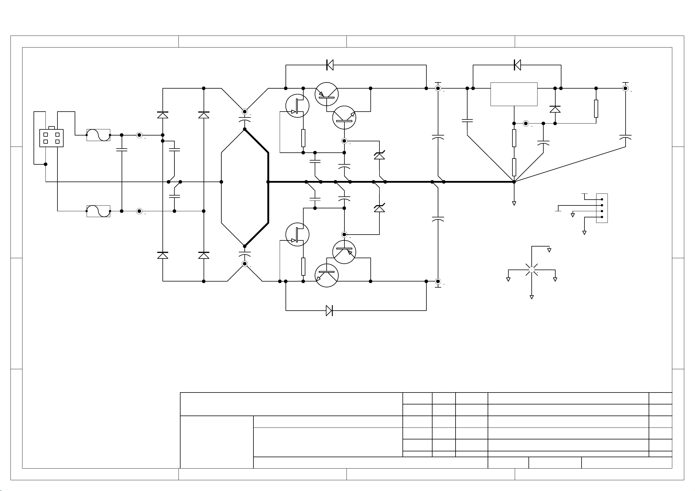
4321
D302
BAS16W SM
Q305
2SA1964
D
C
SK300
MOLEXPWR4
3
4
1
2
F300
T2A SM
F301
T2A SM
AC1
C307
470N PE
AC2
D300
S1D
C308
100N SM
C309
100N SM
D301
S1D
UR+
+
C300
1000u 35V
Q300
J112
R300
330R SM
C314
1N0 PP
C315
1N0 PP
Q303
J112
Q306
BC846B
D310+
+
C302
220U EL
+
C312
220U EL
D311-
D310
15V 350MW SM
D311
15V 350MW SM
+15V
+
+
I
+15V3
C304
100N SM
C303
3300u 25V
C313
3300u 25V
Z301
LM317T
Vin
0V_PSU
D304
BAS16W SM
Vout
ADJ
A
+3.75V
R302
1K2 SM
R307
220R SM
O
+
C305
10U EL
-15V
D305
BAS16W SM
+15V
0V_PSU
0V_MODULE
R303
470R SM
SK301
1
2
3
4
IDC4S
+5V
+5V
+
C306
470U EL 25V
D
C
D306
S1D
B
D307
S1D
+
UR-
C310
1000u 35V
R304
330R SM
Q301
2SC5248
D308
BAS16W SM
Q307
BC856B
-15V
-15V3
SP300
STAR POINT 4
0V_HF 0V_MODULE
0V_PSU
0V SIG
0V_SIG
B
DRAWING TITLE
Integrated amplifier preamp - power supply
A
23425
Notes:
Circuit Diagram
01_E014 JBR 28/11/01 Fuses uprated to 2A 1.1
A
A & R Cambridge Ltd.
Pembroke Avenue
Denny Industrial Centre
Waterbeach
Cambridge CB5 9PB
1 2 3 4
Filename
J:\Change_Control\ECO_AGENDA\01_E014 Fuse changes on A32 preamp\L937_1.1.ddb - Documents\Schematic\L937C3_1.0.SCH
01_1142 JBR 14/8/01 First production release 1.0
ECO No. DESCRIPTION OF CHANGE
Date Printed
INITIALS
28-Nov-2001
DATE
Drawn by:
JBR
3 3Sheet of
DRAWING NO.
L937C3
ISSUE
Page 18
87654321
A85 DISPLAY PCB
D
L865C2_2 0
L865C2_2 0SCH
UDB
Update Box
MICRO
(Small)
UPDATE_SML
D
FD_1
FIDUCIAL
C
B
CHASSIS 1
(BY SK3)
CHASSIS 2
(BY SK1)
0V_D
0V_D
C39
1N0 SM
C45
1N0 SM
FD_2
F DUCIAL
FIX7
FIXING HOLE
FIX1
FIXING HOLE
PCB1
PCB
L865PB_2
FIX2
FIXING HOLE
0V_D 0V_D 0V_D 0V_D 0V_D
FIX8
FIXING HOLE
C40
1N0 SM
C46
1N0 SM
FIX10
FIX NG HOLE
C41
1N0 SM
FIX9
FIXING HOLE
C47
1N0 SM
0V_D0V_D
FIX4
FIXING HOLE
C42
1N0 SM
FIX3
FIXING HOLE
CHASSIS 3
(BY SK2)
FIX5
FIXING HOLE
C43
1N0 SM
FIX11
FIXING HOLE
C48
1N0 SM
0V_D0V_D
FIX6
FIXING HOLE
C49
1N0 SM
C44
1N0 SM
C
B
A
1 2 3 4 5 6 7 8
DRAWING TITLE
MARY AMP DISPLAY PCB
23425
A & R Cambridge Ltd.
Pembroke Avenue
Denny Industrial Centre
Waterbeach
Cambridge CB5 9PB
Notes
Filename
J:\Completed Projects\A85 (Mary)\mary display\L865 2\l865 2.0 dbase.ddb - Documents\L865 2.0.PRJ
Circuit Diagram
ISSUE 1.1
EDD IR DUAL FOOTPRINT ADDED19/07/2001 2 0
00_1103 JBR SW1 TO SW10 CHANGED29 SEP 2000 1.1
ECO No. DESCRIPTION OF CHANGE
Date Printed
INITIALS
8-Jan-2002
DATE
Drawn by:
JBR
1 2Sheet of
DRAWING NO.
L865C1
ISSUE
A
Page 19

8765432
1
+5V
R34
150R SM
LED11
LED RED/GRN 3MM
G
LEFTAUDIO
+5V
R55
10K SM
R51
100R SM
R32
10K SM
5
6WP7
SCL
SDA
VDD
A01A12A2
3
Q2
BC847B
+5V
8
10K SM
IND11
C8
100N SM
R1
10K SM
BUT1
C17
100N SM
PB0
SEL7
SEL6
SEL5
SEL4
SEL3
SEL2
SEL1
VPROG
TRANSMIT
RECEIVE
TONEID
SDATA
SLOAD
SCLK
SW6
A1509
0V_D
0V_D
R2
10K SM
SW12 SW11
BUT2
10U EL SM
C11
+
100K SM
100K SM
+5V
1
2
3
4
5
6
7
8
9
10
11
12
13
14
15
16
17
18
19
20
21
22
23
24
25
0V_D
+5V
C5
100N SM
0V_D
R3
10K SMR410K SM
TACTSW SM
BUT3
5
SW8
A1509
BUT4
Z7B
6
R5
10K SMR610K SM
SW7
A1509
BUT5
7
LM393A SM
0V_D
+5V
R43
R41
R42
100K SM
R44
100K SM
Z7A
LM393A SM
3
2
+5V
R49
1
10K SM
0V_D
PHASEA
PHASEB
SEL8
SEL9
MUTE
100
Vcc
PB0
PB1
PB2
PB3
PB4
PB5
PB6
PB7
Vpp/RESO
Vss
TxD0/P9.0
TxD1/P9.1
RxD0/P9.2
RxD1/P9.3
IRQ4/SCK0/P9.4
IRQ5/SCK1/P9.5
D0/P4.0
D1/P4.1
D2/P4.2
D3/P4.3
Vss
D4/P4.4
D5/P4.5
D6/P4.6
F1CLOCK
F2CLOCK
TONE
88
89
90
91
92
Vss
PA093PA194PA295PA396PA497PA598PA699PA7
P8.4/CS0
P8.2/IRQ2
P8.3/IRQ3
H8/3048F
IRIN
86
87
AVss
P8.0/IRQ0
P8.1/IRQ1
DCPROT
VIPROT
ACPRESENT
82
83
84
85
P7.5/AN5
P7.6/AN6/DA0
P7.7/AN7/DA1
D7/P4.726D8/P3.027D9/P3.128D10/P3.229D11/P3.330D12/P3.431D13/P3.532D14/P3.633D15/P3.734Vcc35A0/P1.036A1/P1.137A2/P1.238A3/P1.339A4/P1.440A5/P1.541A6/P1.642A7/P1.743Vss44A8/P2.045A9/P2.146A10/P2.247A11/P2.348A12/P2.449A13/P2.5
IND12
IND11
BUT16
IND6
BUT15
IND5
BUT10
IND7
BUT12
IND9
BUT14
IND4
BUT11
IND8
BUT13
IND10
0V_D
80
81
P7.2/AN2
P7.3/AN3
P7.4/AN4
IND2
BUT4
TRANSMIT
RECEIVE
78
79
P7.0/AN0
P7.1/AN1
IND1
BUT5
TACTSW SM
SW13
BUT6
R480R0 SM
RECEIVE
VPROG
PB0
+5V
76
77
Vref
AVcc
P6.6/LWR
P6.5/HWR
P6.4/RD
P6.3/AS
EXTAL
CLKOUT
P6.2/BACK
P6.1/BREQ
P6.0/WAIT
P5.3/A19
P5.2/A18
P5.1/A17
P5.0/A16
P2.7/A15
P2.6/A14
H8/3048F
50
BUT3
BUT1
R7
10K SMR810K SM
TACTSW SM
SW14
BUT7
R50
10K SM
C3
100N SM
Z1
75
MD2
74
MD1
73
MD0
72
71
70
69
68
Vcc
67
XTAL
66
65
Vss
64
NM1
63
RES
62
STBY
61
60
59
58
57
Vss
56
55
54
53
52
51
0V_D
CHASSIS 1
+
C14
10U EL SM
0V_D
+5V
C4
100N SM
0V_D
C50B 100PX4 SM
C50D 100PX4 SM
C51B 100PX4 SM
C51D 100PX4 SM
C52B 100PX4 SM
C52D 100PX4 SM
C53B 100PX4 SM
C53D 100PX4 SM
C54B 100PX4 SM
C54D 100PX4 SM
C55B 100PX4 SM
C55D 100PX4 SM
TACTSW SM
SW15
BUT8
SAMHOLD
+5V
+5V
Programming adaptor
R26
10K SM
STANDBY
SP1ON
SP2ON
THERMPROT
RESPIN
SAMTX2
SAMRX2
BUT17
BUT9
BUT8
BUT7
BUT6
BUT2
IND3
0V_D
R68
10K SM
A1506
SW17
5
2V7
6
R37
Z6A
10K SM
1
LM393A SM
C9
100N SM
SK4
12
34
56
78
910
1112
1314
HEADER 7X2HORIZ
D2
BAS16W SM
C50A 100PX4 SM
C50C 100PX4 SM
C51A 100PX4 SM
C51C 100PX4 SM
C52A 100PX4 SM
C52C 100PX4 SM
C53A 100PX4 SM
C53C 100PX4 SM
C54A 100PX4 SM
C54C 100PX4 SM
C55A 100PX4 SM
C55C 100PX4 SM
BUT17
Z6B
LM393A SM
2
3
+5V
R9
10K SM
TACTSW SM
SW16
7
0V5
0V_D
+5V
C7
100N SM
0V_D
FFC 22W 1MM HOR
0V_D
BUT9
+5V
0V_D
TRANSMIT
RESPIN
SAMHOLD
Z2
3
Vcc
2
Res
4
Gnd
1
Gnd
DS1233 SM
To preamp board
SK3
22
21
20
19
18
17
16
15
14
13
12
11
10
9
8
7
6
5
4
3
2
1
R10
10K SM
SW1
A1509
BUT10
R40
4K7 SM
R38
1K2 SM
X1
16MHZ SM
SEL1
SEL2
SEL3
SEL4
SEL5
SEL6
SEL7
SEL8
SEL9
LEFTAUDIO
MUTE
TONE
Q_117
TONEID
Q_118
SDATA
Q_119
SLOAD
Q_120
SCLK
+5V
SAMRX2
C1
18P SM
C2
18P SM
R35
10K SM
0V_D
DS1233
R72
R11
10K SM
BUT11
SAMTX2
R71
2R2 SM
SW4
A1509
+5V
R45
10K SM
R70
2R2 SM
R36
10K SM
2V7
Z8B
7
LM393A SM
C12
100N SM
R69
2R2 SM
0V_D
R12
10K SM
SW2
A1509
BUT12
2R2 SM
0V52V7
Z8A
3
2
LM393A SM
R13
10K SM
SW5
A1509
BUT13
R39
2K2 SM
0V_D
1
0V5
6
5
+5V
+
C33
220U EL
0V_D
(FIT CLOSE TO SK1)
R14
10K SM
SW3
A1509
BUT14
R15
10K SM
SW10
A1509
BUT15
+5V
R47
4K7 SM
SAMBUSYSAMDATA
R46
1K2 SM
0V_D
SBX1610-52/PIC-26043TM2
Q_54
RX1
+5V
2
O/P
O/P
Case
Case
0V_D
+5V
SK2
1
Q_19
Q_20
2
3
4
5
AMPCT5
0V_D
D5
BAS16W SM
Z12
7815
I
Vin
O
Vout
GND
G
C27
100N SM
D4
SAMDATA
SAMBUSY
+
C34
220U EL
+SUP VFD_VDD2
+
C26
10U EL SM
22V 350MW SM
0V_D
DRAWING TITLE
MARY AMP DISPLAY PCB
23425
A & R Cambridge Ltd.
Pembroke Avenue
Denny Industrial Centre
Waterbeach
Cambridge CB5 9PB
R16
10K SM
SW9
A1509
BUT16
R17
1K5 SM
LED7
IND1
LED GREEN3.1MM
R18
1K5 SM
LED8
IND2
LED GREEN3.1MM
LED GREEN3.1MM
R19
1K5 SM
LED6
IND3
LED GREEN3.1MM
R20
1K5 SM
IND4
LED3
IND5
LED GREEN3.1MM
+5V
R74
10K SM
IROUT
R76
10K SM
R75
10K SM
R73
10K SM
Q3
BC847B
IRIN
Q4
BC847B
IRIN
3
R27
10K SM
0V_D
PHASEA
PHASEB
+5V
0V_D
R56
10K SM
R57
10K SM
F1CLOCK
F2CLOCK
+5V
GND
GND +5V
1
SW18
ALPS_ENCODER
4
C6
100N SM
5
+5V
R2810K SM
1
A
2
B
3
C
0V_D
+5V
C60B 100PX4 SM
C60D 100PX4 SM
C61B 100PX4 SM
C61D 100PX4 SM
C62B 100PX4 SM
C62D 100PX4 SM
C63B 100PX4 SM
C63C 100PX4 SM
C63D 100PX4 SM
C60A 100PX4 SM
C60C 100PX4 SM
C61A 100PX4 SM
C61C 100PX4 SM
C62A 100PX4 SM
C62C 100PX4 SM
C63A 100PX4 SM
To power amp / PSU
SK1
14
13
12
11
10
9
8
7
6
5
4
3
2
1
FFC 14W 2.54MM HOR
0V_D
+SUP
Q_121
STANDBY
SP1ON
SP2ON
THERMPRO
VIPROT
DCPROT
ACPRESEN
IRIN
CHASSIS 2
+5V
+
C28
10U EL SM
84
Z6C
LM393A SM
C10
100N SM
84
Z7C
LM393A SM
C15
100N SM
LM393A SM
0V_D
Notes:
Filename
J:\Completed_Projects\A85 (Mary)\mary display\L865_2\l865_2.0 dbase.ddb Documents\L865C2_2.0 SCH
Circuit Diagram
ISSUE 1.1
EDD IR DUAL FOOTPRINT ADDED19/07/2001 2.0
00_1103 JBR 29 SEP 2000 SW1 TO SW10 CHANGED
ECO No. DESCRIPTION OF CHANGE
INITIALS
Date Printed
8-Jan-2002
R21
1K5 SM
LED10
R22
1K5 SM
LED9
IND6
LED GREEN3.1MM
LED GREEN3.1MM
SP1
DOUBLE SIDED
STICKY PAD
10 X 15MM
STICKY PAD DS 10X15MM
SP2
DOUBLE SIDED
STICKY PAD
10 X 15MM
STICKY PAD DS 10X15MM
DC1
DISPLAY CRADLE
E916PM
DISPLAY CRADLE E916PM
DC2
DISPLAY CRADLE
E916PM
DISPLAY CRADLE E916PM
R52
100R SM
R53
100R SM
Q_122
Q_123
Q_124
Q_125
Q_126
Q_127
Q_128
Q_129
84
DATE
C16
100N SM
Drawn by:
JBR
Z8C
R25
1K5 SM
IND7
LED1
IND8
LED GREEN3.1MM
DISP1
R24
1K5 SM
LED4
LED GREEN3.1MM
F1 to F2 = 4Vac 150mA
VDD2 = 40Vdc 20mA
Graphics Display
F11F12F13SIN4VDD15SOUT6LAT7BLK8CLK9VSS10VSS11VDD212F215F216F2
+5V
B1013
DISPDAT
DISPCLK
DISPLAT
DISPBLK
Z11A
AD8532 SM
3
2
5
6
Z11B
AD8532 SM
R58
0R0 SM
R59
7
0R0 SM
84
Z11C
AD8532 SM
2 2Sheet of
R23
1K5 SM
LED2
IND9
LED GREEN3.1MM
0V_D
C25
100N SM
DRAWING NO.
R31
1K5 SM
LED5
IND10
17
VFD_VDD2
+
C29
100U EL SM
L865C2
D
C
B
A
ISSUE
Q1
BC847B
R29
10K SM R30
D
R33
330R SM
IND12
R
0V_D
C
D3
BAS16W SM
DISPDAT
B
DISPCLK
DISPBLK
DISPLAT
C31
10P SM
R64
100R SM
R65
100R SM
R67
100R SM
C32
10P SM
R66
100R SM
0V_D
Z5
24C02 SM
4
VSS
A
0V_D
1 2 3 4 5 6 7 8
Page 20

87654321
D
C
LEFT CHANNEL
C1
100N CD
SK1
PHONO2HG
EMC
1
0V_SIG
0V_SIG
Q_1
Q_2
L870C2_2.0.SCH
LEFT IN LEFT OUT
RIGHT CHANNEL
L870C3 2.0.SCH
RIGHT N RIGHT OUT
Q_3
Q_4
+15V
Q_5
1
2
3
4
5
6
7
Q_6
8
Q_7 Q_8
-15V
0V_HF0V_SIG
SK2
AMPCT8
D
C
B
A
PCB1
PCB
L870PB_2
1 2 3 4 5 6 7 8
EL1
Update Box
UPDATE_BOX
DRAWING TITLE
A85 PHONO STAGE - TOP LEVEL
23425
A & R Cambridge Ltd.
Pembroke Avenue
Denny Industrial Centre
Waterbeach
Cambridge CB5 9PB
Notes
Filename
G:\DATA\ECO\ECO AGENDA\01 1070 l870 A85 PHONO ISSUE2\L870 2.0.ddb - L870c1 2.0.PRJ
Circuit Diagram
01_1070 JAG 17/4/01 updated pcb and scm 2
00_1051 JAG 22/3/01 PRODUCTION ISSUE 1
ECO No. DESCRIPTION OF CHANGE
INITIALS
Date Printed
DATE
Drawn by:
JBR23-Apr-2001
1 3Sheet of
DRAWING NO.
L870C1
B
A
ISSUE
Page 21

87654321
+
C102
100U SILMIC
R111
56K MF
R124
5K6 MF
R123
10R MF
C119
100P PP
C101
1N0 PP
C110
4N7 PP
C120
1N0 PP
C112
10N PP AX
C111
10N PP AX
R112
100K MF
C105
100N PE
Q 101
R113
100K MF
R114
100K MF
R115
15K MF
TL071CD
R101
100R MF
TR102
BC556B
TR108
BC546B
R116
2M2 MF
74
IC100
3
6
C118
2
10U NP
R117
2M2 MF
TR104
BC556B
D
TR100
BC556B
+
C100
22U EL
R109
12K MF
R110
12K MF
LEFT IN
C
R104
100R MF
SW100B
4PCO
5
6
C108
470P PPW
4
R108
47K MF
C109
100P PPW
TR106
2SA1085
R100
330R MF
TR101
BC556B
TR107
2SA1085
C115
N3 PP
SW100D
4PCO
R105
100R MF
101112
Q_102
R102
100R MF
TR103
BC556B
D100
1N4148
C104
100N PE
0V_SIG0V_HF
C106
100N PE
+15V
TR109
BC546B
R118
22R MF
R119
22R MF
TR105
BC556B
C113
1U0 PE
0V_SIG
R122
39K MF
D
C
LEFT OUT
0V_SIG0V_SIG
B
TR110
BC546B
D101
1N4148
R120
22R MF
A
1 2 3 4 5 6 7 8
TR111
BC546B
D102
1N4148
R121
22R MF
DRAWING TITLE
A85 PHONO STAGE - LEFT CHANNEL
A & R Cambridge Ltd.
Pembroke Avenue
Denny Industrial Centre
Waterbeach
Cambridge CB5 9PB
C116
470P PPW
23425
TR112
BC546B
+
C103
100U SILMIC
Notes
Filename
G:\DATA\ECO\ECO AGENDA\01 1070 l870 A85 PHONO ISSUE2\L870 2.0.ddb - L870C2 2.0.SCH
TR113
BC546B
TR114
BC546B
R106
100R MF
0V_SIG0V_HF
Circuit Diagram
C117
470P PPW
C107
100N PE
Q_103
-15V
01_1070 JAG 17/4/01 updated pcb and scm 2
00_1051 JAG 22/3/01 PRODUCTION ISSUE 1
ECO No. DESCRIPTION OF CHANGE
INITIALS
Date Printed
DATE
Drawn by:
JBR23-Apr-2001
2 3Sheet of
DRAWING NO.
L870C2
B
A
ISSUE
Page 22

87654321
+
C202
100U SILMIC
R211
56K MF
R224
5K6 MF
9
R223
10R MF
C219
100P PP
C201
1N0 PP
C210
4N7 PP
C220
1N0 PP
C212
10N PP AX
C211
10N PP AX
R212
100K MF
C205
100N PE
Q 201
R213
100K MF
R214
100K MF
R215
15K MF
TL071CD
R201
100R MF
TR202
BC556B
TR208
BC546B
R216
2M2 MF
74
IC200
6
3
2
C218
10U NP
R217
2M2 MF
TR204
BC556B
D
TR200
BC556B
+
C200
22U EL
R209
12K MF
R210
12K MF
RIGHT IN
C
R204
100R MF
SW100A
4PCO
2
3
C208
470P PPW
1
R208
47K MF
C209
100P PPW
TR206
2SA1085
R200
330R MF
TR201
BC556B
TR207
2SA1085
R205
100R MF
C215
1N3 PP
7
SW100C
4PCO
8
Q_202
R202
100R MF
TR203
BC556B
D200
1N4148
C204
100N PE
0V_SIG0V_HF
C206
100N PE
+15V
TR209
BC546B
R218
22R MF
R219
22R MF
TR205
BC556B
C213
1U0 PE
0V_SIG
R222
39K MF
D
C
RIGHT OUT
C217
0V_SIG0V_SIG
B
TR210
BC546B
D201
1N4148
R220
22R MF
A
TR211
BC546B
D202
1N4148
R221
22R MF
DRAWING TITLE
A85 PHONO STAGE - RIGHT CHANNEL
23425
A & R Cambridge Ltd.
Pembroke Avenue
Denny Industrial Centre
Waterbeach
1 2 3 4 5 6 7 8
Cambridge CB5 9PB
470P PPW
TR212
BC546B
+
C203
100U SILMIC
Notes
Filename
G:\DATA\ECO\ECO AGENDA\01 1070 l870 A85 PHONO ISSUE2\L870 2.0.ddb - L870C3 2.0.SCH
TR213
BC546B
TR214
BC546B
R206
100R MF
0V_SIG0V_HF
Circuit Diagram
470P PPWC216
C207
100N PE
Q_203
-15V
01_1070 JAG 17/4/01 updated pcb and scm 2
00_1051 JAG 22/3/01 PRODUCTION ISSUE 1
ECO No. DESCRIPTION OF CHANGE
INITIALS
Date Printed
DATE
Drawn by:
JBR23-Apr-2001
3 3Sheet of
DRAWING NO.
L870C3
B
A
ISSUE
Page 23

87654321
+5V_D
1
2
3
4
5
SPKR1 ON
6
SPKR2 ON
7
THERMPROT
8
VIPROT1
9
DCPROT1
10
11
12
13
14
TP102
TP103
+5V_D
TP104
TP105
TP106
TP107
TP108
0V_D
0V_D
0V_SIG
TP116
0V_LS 0V_HF
SP100
STAR POINT 8
0V_PSU
R107
2R2 SM
D
0V_D
SK100
D
+5V_D
14
IC100G
74HC14D
7
C100
100N SM
+
C102
100U EL
C101
100N SM
R100
1K0 SM
TH100
PTH90DEG
IC100E
74HC14D
IC100F
1011
1213
FFC 14W 2.54MM VER
PIN 1 TO THE LEFT AS YOU LOOK FROM THE FRONT
THERMPROT
0V_D
C
+49V
D100
1N4003F
TR100
BD179
B
RLY101B
RLY SPST SPKR
R103
220R SM
0V_D
TR101
BD179
RLY100B
RLY SPST SPKR
R105
100R SM
R106
100R SM
R104
220R SM
74HC14D
D101
1N4003F
SPKR1 ON
SPKR2 ON
0V_SIG
EMC
C105
1N0 SM
TP110
SK101
F
N
PHONO2G
1
TP109
+49V
-49V
0V_HF
0V_LS
L911C2_1
L911C2_1.1.SCH
INPUT
0V_SIG
0V_HF
VPOS
VNEG
VIPROT
DCPROT
OUTPUT0V_LS
R101
1K0 SM
R102
1K0 SM
TP111
1 2
C103
10N SM
5 6
C104
10N SM
0V_D
RLY101A
RLY SPST SPKR
TP112 TP113
IC100A
74HC14D
IC100C
74HC14D
3 4
SK102A
Top+
Top-
0V_LS
IC100B
74HC14D
IC100D
74HC14D
RLY100A
RLY SPST SPKR
C
VIPROT1
89
DCPROT1
SK102B
Bot+
Bot-
B
+49V
TP100
1
BR100
TP114
1
2
SK103
3
A
MOLEXPWR4
4
TP115
1 2 3 4 5 6 7 8
3
BRGBU8D
+
2
~
~
-
4
-49V
+
C106
10,000u 63V
+
C107
10,000u 63V
C108
100N PC
0V_PSU
C109
100N PC
POWER AMP SUPPLY
TP101
PB
PCB
L911PB_1
DRAWING TITLE
AP85 third channel - top level
23425
A & R Cambridge Ltd.
Pembroke Avenue
Denny Industrial Centre
Waterbeach
Cambridge CB5 9PB
Notes:
Filename
J:\ECO wip\01 1101 A85 RANGE PCB FUSES AND DC OFFSET\L911 1.1.DDB - Documents\ 911C1 1.1.PRJ
Circuit Diagram
01_1101 JR 4/6/01 DC OFFSET CHANGES 1.1
01_1018
ECO No. DESCRIPTION OF CHANGE
Date Printed
JR 30/1/01 PRODUCTION ISSUE 1.0
INITIALS
4-Jun-2001
DATE
Drawn by:
J Reckless
1 2Sheet of
DRAWING NO.
L911C1
ISSUE
A
Page 24

87654321
D
R315
TR300
FMMT597
C310
100N SM
3
2
C314
100N SM
TR314
FMMT497
100R SM
PNP CURRENT MIRROR
TR311
FMMT497
R328
4K7 SM
TP302
84
0V_SIG
IC300A
TL072CD
TP303
TR303
FMMT597
NPN CURRENT MIRROR
R317
100R SM
R300
10K SM
+
C300
DZ300
100U EL
15V 350MW SM
0V_HF
0V_SIG
C
INPUT
0V SIG
0V_HF
B
NPUT FILTER V TO I AMP
R324
1K0 SM
DZ302
4V7 350MW SM
DZ303
4V7 350MW SM
0V_SIG
+
C301
100U EL
0V_HF
C309
100N SM
DZ301
15V 350MW SM
R309
10K SM
R327
22K SM
C316
470P PPW
0V_SIG
7
1
C317
470N PE
IC300B
TL072CD
R322
22R SM
R337
22R SM
0V_SIG
R319
100R SM
R333
3K3 SM
DC SERVO
0V_SIG
TP304
R335
3K3 SM
R320
100R SM
R330
6
1M0 SM
5
R331
1K5 SM
R332
1K8 SM
C307
100P SM
TR322
FMMT497
C311
100N PC
C308
100P SM
R316
100R SM
TR301
FMMT597
TR321
FMMT597
R355
6K8 SM
R354
1K0 SM
TR320
FMMT497
TR315
FMMT497
R318
100R SM
TR309
FMMT497
R338
150R SM
BOOTSTRAP
+
C302
100U EL 100V
R352
470R 2W
470R 2W
R353
+
C318
10U EL
+
C306
100U EL 100V
BOOTSTRAP
R339
150R SM
TR306
FMMT597
PRE DRIVER
TR310
FMMT497
R321
22R SM
C312
10N SM
R323
22R SM
TR307
FMMT597
PRE DRIVER
ADJ BIAS
RV300
100R PSET
D300
BAS16W SM
OUTPUT STAGE
TR318
SAP15N
TP305
R325
1K0 SM
R340
100K SM
R326
1K0 SM
TP306
TR319
SAP15P
OUTPUT STAGE
PL300
1
2
MEASURE
BIAS
R341
330R SM
R342
330R SM
R343
100R SM
R344
100R SM
V-I PROTECTION
R334
22K SM
R347
100R SM
R345
0R0 SM
+
C303
100U EL
+
C304
100U EL
R346
0R0 SM
R348
100R SM
R336
22K SM
V-I PROTECTION
D301
BAS16W SM
TR312
FMMT497
TR304
FMMT597
D302
BAS16W SM
D303
1N4003F
DC OFFSET SIGNAL
TO MICRO
D304
1N4003F
0V_HF
R349
100R SM
DCPROT
TR305
FMMT597
TP308
DZ306
4V7 350MW SM
R302
10K SM
R310
4K7 SM
C315
100N SM
R301
10K SM
R329
4K7 SM
TR313
FMMT497
R303
10K SM
R304
10K SM
R311
10K SM
R312
10K SM
0V_HF
TR316
FMMT497
TR308
FMMT597
TR302
FMMT597
R305
10K SM
R306
10K SM
DC OFFSET
DETECTION
R307
10K SM
R313
10K SM
TR317
FMMT497
VI PROTECT
SIGNAL TO MICRO
TP307
R308
22K SM
C320
100U NP
DZ305
4V7 350MW SM
+
C305
10U EL
VIPROT
R351
5R6 2W CF
L300
2U2H LAC SMALL
R350
5R6 2W CF
ZOBEL NETWORK
C319
100N PE
0V_HF 0V_LS
R314
10K SM
C313
100N SM
VPOS
OUTPUT
0V LS
0V HF
VNEG
D
C
B
A
A
DRAWING TITLE
AP85 third channel - output stage
23425
A & R Cambridge Ltd.
Pembroke Avenue
Denny Industrial Centre
Waterbeach
Cambridge CB5 9PB
1 2 3 4 5 6 7 8
Notes:
Filename
L911C2 1.1.SCH
Circuit Diagram
01_1101 JR 4/6/01 DC OFFSET CHANGES 1.1
JR 30/1/01 PRODUCTION ISSUE 1.001_1018
INITIALS
DATE
Drawn by:
J Reckless4-Jun-2001
2 2Sheet of
DRAWING NO.
L911C2
ECO No. DESCRIPTION OF CHANGE
Date Printed
ISSUE
Page 25

+5V_D
87654321
R1
SK1
+5V_D
14
13
SK2
12
11
10
9
8
7
6
5
4
3
2
1
0V_D
+5V_D
14
13
12
11
10
9
8
7
6
5
4
3
2
1
R9
10K MF
R10
10K MF
STANDBY
SPKR1 ON
SPKR2 ON
THERMPROT 1
VIPROT 1
DCPROT 1
AC PRESENT
TRIGGER
REMOTE
SPKR1 ON
SPKR2 ON
THERMPROT 2
VIPROT 2
DCPROT 2
R11
10K MF
SP2 SW
SP1 SW
SP1 LED
SPKR2 ON
SPKR1 ON
STANDBY
PWR SW
REMOTE
TRIGGER
AC PRESENT
THERMPROT
Z1
1
PB5
2
PB4
3
PA3
4
PA2
5
PA1
6
PA0
7
PB3
8
PB2
9
PB1
10
PB0
11
VSS
12
(TMR)/ NT
13
PC0
14
PC1
HT48R30 28-DIP-B-0
PB6
PB7
PA4
PA5
PA6
PA7
OSC2
OSC1
VDD
RES
PC5
PC4
PC3
PC2
28
27
26
25
24
23
22
21
20
19
18
17
16
15
DCPROT
VIPROT
SP2 LED
PWR GRN
PWR RED
C1
100N CD
D1
1N4148
+5V_D
0V_D
R16
100K MF
+
C5
10U EL
X1
CST4 00
D
C
10K MF
R2
10K MF
SP2 LED
Q1
BC556BR310K MF
R4
10K MF
R12
560R MF
LED1 LED2
SP1 LED
SW1
A1503
10K MF
Q2
BC556B
10K MF
R13
560R MF
R5
R6
SW2
A1503
330R MF
PWR RED
Q4
BC556B
R14
R
0V_D
SW3
A1506
Q3
BC556B
R15
180R MF
G
LED3
R7
10K MF
R8
10K MF
PWR GRN
D
C
0V_D
0V_D
Z2A
1
2
4
5
74HC32
Z2B
3
6
THERMPROT
VIPROT
+5V_D
C14
100U EL
+5V_D
THERMPROT 1
THERMPROT 2
SPKR1 ON
+
R19
470R MF
Q5
BC546B
VIPROT 1
VIPROT 2
74HC32
D2
1N4148
R17
10K MF
B
R20
0V_D
Q6
BC546B
SPKR2 ON
DCPROT 1
DCPROT 2
10
9
Z2C
74HC32
8
DCPROT
C2
100N CD
C3
100N CD
0V_D
SP2 SW
+
C4
100N CD
C6
100U EL
BY SK1 BY SK2 BY Z1
+
C7
100U EL
SP1 SW
+
C8
100U EL
PWR SW
GND
7
14
VDD
Z2E
74HC32
12
13
Z2D
74HC32
11
B
470R MF
R18
10K MF
R21
0V_D
Q7
BC546B
STANDBY
FIX1
FIX NG HOLE
470R MF
TL1
0V_D
A
EL1
CLOGO
Layout by
Cliff
DD1
PCB MATERIAL
FR4, 1 OZ Cu
FR4_1OZ
0V_D
PS
Photo Strip
PHOTO_STR P
PCB
L910PB_1
PCB
DD2
Drilling
Detail
DRILL_DWG
EL2
Update Box
UPDATE_BOX
TOOL NG
DD3
A3 Vertical
Paper Marker
DD_A3V
TL2
TOOLING
DRAWING TITLE
P85 microcontroller and switch
A & R Cambridge Ltd.
Pembroke Avenue
Denny Industrial Centre
Waterbeach
Cambridge CB5 9PB
C9
100N CD
FIX2
FIXING HOLE
C10
100N CD
FIX3
FIX NG HOLE
C11
100N CD
FIX4
FIXING HOLE
C12
100N CD
FIX5
FIXING HOLE
0V_D
Notes
Filename
J:\ECO wip\00 1099 L910PB 1.0\L910AY 1\L910AY 1.ddb - L910CT 1 sch
Circuit Diagram
C13
100N CD
00_1099
ECO No. DESCRIPTION OF CHANGE
Date Printed
CL 28/09/00 PRODUCTION RELEASE 1 0
INITIALS
29-Sep-2000
DATE
Drawn by:
CG
1 1Sheet of
DRAWING NO.
A
ISSUE
L910CT
1 2 3 4 5 6 7 8
Page 26

Page 27

Page 28

Page 29

Page 30

Page 31

Page 32

Page 33

ARCAM PCB Bill of Materials
Document title: A85 POWER AMPLIFIER AND PSU
Document number: L882RS Issue: 3 Revision: 2 ECO number: 01_1101A
Date: 06/06/01 Created by: JR Page 1 of 3
(Excluding parts for NF.)
Part Qty Iss Description Designators
******** PCB Finish items:
******** (For drawing office use only. Will be
******** kitted from mechanical run-out sheet.)
C12207 2 FUSE 20mm 2A AS F200 F201
F022 2 INS COVER PCB FUSEHOLDER F200 F201
******** PCB Build items:
1A000 4 RES SM W4 1% 0R0 1206 R345 R346 R445 R446
1A010 3 RES SM W4 1% 10R 1206 R217 R220 R221
1A022 8 RES SM W4 1% 22R 1206 R321 R322 R323 R337
R421 R422 R423 R437
1A110 24 RES SM W4 1% 100R 1206 R101 R102 R315 R316
R317 R318 R319 R320
R343 R344 R347 R348
R349 R415 R416 R417
R418 R419 R420 R443
R444 R447 R448 R449
1A115 4 RES SM W4 1% 150R 1206 R338 R339 R438 R439
1A122 2 RES SM W4 1% 220R 1206 R107 R108
1A133 4 RES SM W4 1% 330R 1206 R341 R342 R441 R442
1A147 1 RES SM W4 1% 470R 1206 R226
1A210 17 RES SM W4 1% 1K0 1206 R200 R201 R202 R203
R204 R205 R206 R207
R227 R324 R325 R326
R354 R424 R425 R426
R454
1A215 3 RES SM W4 1% 1K5 1206 R230 R331 R431
1A218 5 RES SM W4 1% 1K8 1206 R219 R224 R225 R332
R432
1A233 4 RES SM W4 1% 3K3 1206 R333 R335 R433 R435
1A247 11 RES SM W4 1% 4K7 1206 R212 R213 R214 R215
R216 R310 R328 R329
R410 R428 R429
1A268 2 RES SM W4 1% 6K8 1206 R355 R455
1A310 33 RES SM W4 1% 10K 1206 R208 R209 R210 R211
R218 R222 R223 R300
R301 R302 R303 R304
R305 R306 R307 R309
R311 R312 R313 R314
R400 R401 R402 R403
R404 R405 R406 R407
R409 R411 R412 R413
R414
1A322 8 RES SM W4 1% 22K 1206 R308 R327 R334 R336
R408 R427 R434 R436
1A410 4 RES SM W4 1% 100K 1206 R228 R229 R340 R440
1A510 2 RES SM W4 1% 1M0 1206 R330 R430
1C856 2 RES CF 2W 5R6 5% R350 R450
1E110 2 RES CF 1W 100R 5% R105 R106
1E133 2 RES CF 1W 330R 5% R103 R104
1H010 3 RES MF W4 1% 10R R100 R351 R451
1J147 4 RES 2W MF 5% 470R R352 R353 R452 R453
1K515 1 RES W25 5% VR25 1M5 R231
1T002 1 THERMISTOR SIEMENS B59008 TH200
Page 34

ARCAM PCB Bill of Materials
Document title: A85 POWER AMPLIFIER AND PSU
Document number: L882RS Issue: 3 Revision: 2 ECO number: 01_1101A
Date: 06/06/01 Created by: JR Page 2 of 3
2A410 3 CERD 100N 63V 20% RA C224 C225 C226
2C110 4 MLC 100P 50V NPO 5% SM C307 C308 C407 C408
2C210 3 MLC 1N0 50V X7R 10% SM C100 C231 C235
2C310 11 MLC 10N 50V X7R 10% SM C213 C214 C215 C216
C217 C218 C219 C221
C230 C312 C412
2C410 16 MLC 100N 50V X7R 10% SM C201 C202 C203 C204
C220 C232 C309 C310
C313 C314 C315 C409
C410 C413 C414 C415
2D147W 2 PPRO W 470P 63V 5% RA C316 C416
2D168 1 PPRO 680P 5% 63V RA C200
2D422 1 220NF CLASS X2 CAP 275VRMS C234
2H410 4 PCRB 100N 100V 10% RA 5mm C211 C212 C311 C411
2K233 4 SUPPR CAP 3N3 250V C205 C206 C207 C208
2K410 2 PEST 100N 63V 10% C319 C419
2K447 2 PEST 470N 63V 10% C317 C417
2N610 7 ELST 10U 50V C222 C223 C233 C305
C318 C405 C418
2N622 1 ELST 22U 63V C229
2N710 8 ELST 100U 25V C300 C301 C303 C304
C400 C401 C403 C404
2N710B 4 ELST 100U 100V C302 C306 C402 C406
2N810A 1 ELST 1M0 10V C228
2N833 1 ELST 3M3 25V C227
2N910A 2 ELST 10m 63V RA 35mm C209 C210
2V710 2 ELST NON POLAR 100UF 16V C320 C420
3AS16W 8 DIODE SS SM BAS16W D205 D206 D300 D301
D302 D400 D401 D402
3B4003 10 RECTIFIER 1N4003F 1A 200V D100 D101 D200 D201
D202 D203 D303 D304
D403 D404
3BGBU8D 1 BRIDGE RECTIFIER 8A 200V BR200
3CW315V 5 ZENER 15V OW35 SM SOT23 DZ207 DZ300 DZ301
DZ400 DZ401
3CW34V7 9 ZENER 4V7 OW 35 SM SOT23 DZ204 DZ302 DZ303
DZ305 DZ306 DZ402
DZ403 DZ405 DZ406
4A849B 1 TRANS LF SS N SM BC849B TR204
4A856B 2 TRANS LF SS P SM BC856B TR205 TR206
4AFMMT497 24 TRANS LF SS N SM FMMT497 TR201 TR203 TR309
TR310 TR311 TR312
TR313 TR314 TR315
TR316 TR317 TR320
TR322 TR409 TR410
TR411 TR412 TR413
TR414 TR415 TR416
TR417 TR420 TR422
4AFMMT597 21 TRANS LF SS P SM FMMT597 TR202 TR300 TR301
TR302 TR303 TR304
TR305 TR306 TR307
TR308 TR321 TR400
TR401 TR402 TR403
TR404 TR405 TR406
TR407 TR408 TR421
4B179 3 NPN TRANS MP BD179 TR100 TR101 TR200
4CSAP15N 2 TRANS POWER NPN SAP15N TR318 TR418
4CSAP15P 2 TRANS POWER PNP SAP15P TR319 TR419
5B072D 2 IC AUDIO SM DUAL TL072 IC300 IC400
Page 35

ARCAM PCB Bill of Materials
Document title: A85 POWER AMPLIFIER AND PSU
Document number: L882RS Issue: 3 Revision: 2 ECO number: 01_1101A
Date: 06/06/01 Created by: JR Page 3 of 3
5D7805 1 IC VREG POS 7805 IC201
5J7414D 1 SURFACE MOUNT HEX SCHMITT TRIGGER IC202
5M393AD 1 IC COMPARATOR SM DUAL LM393A IC200
6F110 2 PRES 100R LIN HORIZ RV300 RV400
7A9301 1 TRANSFORMER 3VA 9V+9V TYPE 9301 TX200
7D002C 2 INDUCT 2U2 12x20mm L300 L400
7D327 1 27mH INDUCTOR L200
8A001 1 IEC MAINS CONN PCB INS PX SK203
8D225 1 PHONO SKT 4-WAY EMC GOLD SK104
8D301 1 STEREO JACK PCB SK105
8D302 1 MIN JACK DUAL 3.5mm HSJ1002-01-1020 SK201
8D418G 2 CAMCON BINDING POST 4WAY GOLD SK100 SK101
8K2306 1 MOLEX MINI FIT HCS 6 WAY SK200
8K2308 1 MOLEX MINI FIT HCS 8 WAY SK204
8K2404 3 4-WAY AMP CT CONN SK102 SK106 SK107
8K2406 1 6-WAY AMP CT CONN SK205
8K6201 4 2WAY MOLEX VERT MALE CONNECTOR PL100 PL101 PL300
PL400
8K7014 1 FFC 14W 2.54MM VER PTH SK103
8M101 1 EARTH LEAD EL
8Q003 1 CAGE CLAMP 16A 1 WAY ARC003-236 SK202
8S004 2 FUSEHOLDER 20mm PCB F200 F201
A1008 1 SW PUSH 2PCO SW100
A1404 1 VOLTAGE SELECTOR SLIDE SWITCH SW200
A207 2 RELAY G5Z-2A-E 24V RLY100 RLY101
A219 1 RELAY MAINS DPDT 5V 5A RLY200
C3751 1 FUSE R452 T750mA F202
E5402 1 MAINS EMC SHIELD SH200
F006 1 HEATSINK CLIP TO220 13/8.6 DC/W HS200
F008 1 HEATSINK TO220 8.6 DEGC/W HS200
L882PB_3 1 X PRINTED CIRCUIT BOARD PCB
******** Obsolete, absent, redundant, or incorrect issue in PDM:
L882PB_3 1 X PRINTED CIRCUIT BOARD PCB
***************************************************************************
*********************** Additions Since Last Issue ************************
***************************************************************************
Part Qty Iss Description Designators
1A310 2 RES SM W4 1% 10K 1206 R314 R414
1A322 2 RES SM W4 1% 22K 1206 R308 R408
C3751 1 FUSE R452 T750mA F202
***************************************************************************
*********************** Deletions Since Last Issue ************************
***************************************************************************
Part Qty Iss Description Designators
1A247 2 RES SM W4 1% 4K7 1206 R314 R414
1A310 2 RES SM W4 1% 10K 1206 R308 R408
C3501 1 FUSE R452 T500mA F202
Page 36

ARCAM PCB Bill of Materials
Document title: A85 PREAMPLIFIER
Document number: L866RS Issue: 3 Revision: 1 ECO number: 01_1101
Date: 06/06/01 Created by: JR Page 1 of 3
(Excluding parts for NF.)
Part Qty Iss Description Designators
1A022 1 RES SM W4 1% 22R 1206 R185
1A047 6 RES SM W4 1% 47R 1206 R108 R109 R133 R134
R186 R187
1A122 1 RES SM W4 1% 220R 1206 R307
1A133 2 RES SM W4 1% 330R 1206 R300 R304
1A147 1 RES SM W4 1% 470R 1206 R303
1A210 14 RES SM W4 1% 1K0 1206 R100 R101 R102 R125
R126 R127 R156 R157
R158 R189 R190 R191
R195 R196
1A212 1 RES SM W4 1% 1K2 1206 R302
1A222 4 RES SM W4 1% 2K2 1206 R110 R111 R135 R136
1A227 4 RES SM W4 1% 2K7 1206 R115 R116 R140 R141
1A247 1 RES SM W4 1% 4K7 1206 R203
1A256 2 RES SM W4 1% 5K6 1206 R117 R142
1A310 4 RES SM W4 1% 10K 1206 R181 R182 R188 R204
1A322 41 RES SM W4 1% 22K 1206 R112 R113 R114 R118
R119 R120 R121 R137
R138 R139 R143 R144
R145 R146 R147 R148
R149 R150 R151 R152
R153 R154 R155 R162
R163 R164 R165 R166
R167 R168 R169 R170
R171 R172 R173 R174
R175 R176 R177 R178
R179
1A410 16 RES SM W4 1% 100K 1206 R103 R104 R105 R128
R129 R130 R159 R160
R161 R180 R192 R193
R194 R197 R198 R199
1A510 6 RES SM W4 1% 1M0 1206 R106 R107 R131 R132
R183 R184
1A822 6 RES SM W4 1% 2R2 1206 R122 R123 R124 R200
R201 R202
2C022 6 MLC 22P 50V NPO 5% SM C115 C136 C148 C149
C158 C159
2C110 4 MLC 100P 50V NPO 5% SM C108 C109 C129 C130
2C210 6 MLC 1N0 50V X7R 10% SM C100 C121 C139 C160
C164 C186
2C310 1 MLC 10N 50V X7R 10% SM C119
2C410 36 MLC 100N 50V X7R 10% SM C104 C105 C106 C107
C118 C125 C126 C127
C128 C143 C144 C145
C146 C152 C153 C155
C156 C168 C169 C170
C171 C172 C173 C174
C175 C176 C177 C178
C179 C180 C181 C182
C183 C184 C185 C304
2D147W 14 WIMA FKP2 470P 63V CAP C101 C102 C103 C122
C123 C124 C140 C141
C142 C161 C162 C163
C165 C166
Page 37

ARCAM PCB Bill of Materials
Document title: A85 PREAMPLIFIER
Document number: L866RS Issue: 3 Revision: 1 ECO number: 01_1101
Date: 06/06/01 Created by: JR Page 2 of 3
2D210 2 PPRO 1N0 5% 63V RA C314 C315
2D222W 2 WIMA FKP2 2N2 63V CAP C114 C135
2H410 2 PCRB 100N 100V 10% RA 5mm C147 C167
2K447 8 PEST 470N 63V 10% C112 C113 C133 C134
C150 C151 C192 C193
2N610 8 ELST 10U 50V C120 C154 C187 C188
C189 C190 C191 C305
2N710 3 ELST 100U 25V C110 C131 C157
2N722 2 ELST 220U 16V C302 C312
2N747 1 ELST 470U 25V RA C306
2N810C 2 ELST 1M0 35V C300 C310
2N833 2 ELST 3M3 25V C303 C313
2P610CC 6 ELEC 10U 50V CERAFINE C111 C116 C117 C132
C137 C138
3AS16W 5 DIODE SS SM BAS16W D120 D302 D304 D305
D308
3AV99W 22 DIODE SS SM BAV99W D100 D101 D102 D103
D104 D105 D106 D107
D108 D109 D110 D111
D112 D113 D114 D115
D116 D117 D118 D119
D121 D122
3BS1D 4 RECT S1D 1A 200V SM D300 D301 D306 D307
3CW315V 2 ZENER 15V OW35 SM SOT23 D310 D311
4A846B 1 TRANS LF SS N SM BC846B Q306
4A849B 1 TRANS LF SS N SM BC849B Q100
4A856B 1 TRANS LF SS P SM BC856B Q307
4B1964 1 TRANS AUDIO DRIVER P 2SA1964 Q305
4B5248 1 TRANS AUDIO DRIVER N 2SC5248 Q301
4J112 2 TRANS JFET N J112 Q300 Q303
5A1844 1 IC DS1844S-010 Z108
5AVSDVC 1 IC AUDIO DIGITAL VOL SM Z107
5B072D 6 IC AUDIO SM DUAL TL072 Z109 Z110 Z111 Z112
Z113 Z114
5B2134 3 IC OPAMP DUAL SM OPA2134PA Z115 Z116 Z117
5D317T 1 IC VREG POS LM317T Z301
5S408DY 6 IC 8 TO 1 MUX DG408DY SO16 Z100 Z101 Z102 Z103
Z104 Z105
5S413DY 1 IC QUAD SPST CMOS SW SO16 Z106
8D225 4 PHONO SKT 4-WAY EMC GOLD SK2 SK3 SK4 SK5
8D226 1 PHONO SKT 2-WAY EMC GOLD SK6
8K2304 1 MOLEX MINI FIT HCS 4 WAY SK300
8K2404 1 4-WAY AMP CT CONN SK102
8K2408 1 8-WAY AMP CT CONN SK103
8K6604 1 4-WAY FR LOCK CONN SK301
8K8322 1 22-WAY FFC CONN SM 1mm SK100
8K8330 1 30-WAY FFC VERT CONN SM 1MM SK101
A216 1 RELAY DPDT 5V SM NEC EB2-5NU RLY100
C3751 2 FUSE R452 T750mA F300 F301
L866PB_3 1 X PRINTED CIRCUIT BOARD PCB1
Page 38

ARCAM PCB Bill of Materials
Document title: A85 PREAMPLIFIER
Document number: L866RS Issue: 3 Revision: 1 ECO number: 01_1101
Date: 06/06/01 Created by: JR Page 3 of 3
******** Obsolete, absent, redundant, or incorrect issue in PDM:
L866PB_3 1 X PRINTED CIRCUIT BOARD PCB1
***************************************************************************
*********************** Additions Since Last Issue ************************
***************************************************************************
Part Qty Iss Description Designators
C3751 2 FUSE R452 T750mA F300 F301
***************************************************************************
*********************** Deletions Since Last Issue ************************
***************************************************************************
Part Qty Iss Description Designators
C3501 2 FUSE R452 T500mA F300 F301
Page 39

ARCAM PCB Bill of Materials
Document title: A85 / A32 Integrated amplifier preamp PCB
Document number: L937RS Issue: 1 Revision: 1 ECO number: 01_E014
Date: 28/11/01 Created by: J Reckless Page 1 of 2
Part Qty Iss Description Designators
1A022 1 RES SM W4 1% 22R 1206 R185
1A047 6 RES SM W4 1% 47R 1206 R108 R109 R133 R134
R186 R187
1A110 1 RES SM W4 1% 100R 1206 R182
1A122 1 RES SM W4 1% 220R 1206 R307
1A133 2 RES SM W4 1% 330R 1206 R300 R304
1A147 1 RES SM W4 1% 470R 1206 R303
1A210 14 RES SM W4 1% 1K0 1206 R100 R101 R102 R125
R126 R127 R156 R157
R158 R189 R190 R191
R195 R196
1A212 1 RES SM W4 1% 1K2 1206 R302
1A222 4 RES SM W4 1% 2K2 1206 R110 R111 R135 R136
1A227 4 RES SM W4 1% 2K7 1206 R115 R116 R140 R141
1A247 1 RES SM W4 1% 4K7 1206 R203
1A256 2 RES SM W4 1% 5K6 1206 R117 R142
1A310 3 RES SM W4 1% 10K 1206 R181 R188 R204
1A322 41 RES SM W4 1% 22K 1206 R112 R113 R114 R118
R119 R120 R121 R137
R138 R139 R143 R144
R145 R146 R147 R148
R149 R150 R151 R152
R153 R154 R155 R162
R163 R164 R165 R166
R167 R168 R169 R170
R171 R172 R173 R174
R175 R176 R177 R178
R179
1A410 16 RES SM W4 1% 100K 1206 R103 R104 R105 R128
R129 R130 R159 R160
R161 R180 R192 R193
R194 R197 R198 R199
1A510 6 RES SM W4 1% 1M0 1206 R106 R107 R131 R132
R183 R184
1A822 6 RES SM W4 1% 2R2 1206 R122 R123 R124 R200
R201 R202
2C022 6 MLC 22P 50V NPO 5% SM C115 C136 C148 C149
C158 C159
2C110 4 MLC 100P 50V NPO 5% SM C108 C109 C129 C130
2C210 5 MLC 1N0 50V X7R 10% SM C100 C121 C139 C160
C164
2C310 1 MLC 10N 50V X7R 10% SM C119
2C410 39 MLC 100N 50V X7R 10% SM C104 C105 C106 C107
C118 C125 C126 C127
C128 C143 C144 C145
C146 C152 C153 C155
C156 C168 C169 C170
C171 C172 C173 C174
C175 C176 C177 C178
C179 C180 C181 C182
C183 C184 C185 C186
C304 C308 C309
2D147W 14 WIMA FKP2 470P 63V CAP C101 C102 C103 C122
C123 C124 C140 C141
C142 C161 C162 C163
C165 C166
Page 40

ARCAM PCB Bill of Materials
2210 SK100
Document title: A85 / A32 Integrated amplifier preamp PCB
Document number: L937RS Issue: 1 Revision: 1 ECO number: 01_E014
Date: 28/11/01 Created by: J Reckless Page 2 of 2
2D210 2 PPRO 1N0 5% 63V RA C314 C315
2D222W 2 WIMA FKP2 2N2 63V CAP C114 C135
2K410 2 PEST 100N 63V 10% C147 C167
2K447 9 PEST 470N 63V 10% C112 C113 C133 C134
C150 C151 C192 C193
C307
2N610 8 ELST 10U 50V C120 C154 C187 C188
C189 C190 C191 C305
2N710 3 ELST 100U 25V C110 C131 C157
2N722 2 ELST 220U 16V C302 C312
2N747 1 ELST 470U 25V RA C306
2N810C 2 ELST 1M0 35V C300 C310
2N833 2 ELST 3M3 25V C303 C313
2P610CC 6 ELEC 10U 50V CERAFINE C111 C116 C117 C132
C137 C138
3AS16W 5 DIODE SS SM BAS16W D120 D302 D304 D305
D308
3AV99W 22 DIODE SS SM BAV99W D100 D101 D102 D103
D104 D105 D106 D107
D108 D109 D110 D111
D112 D113 D114 D115
D116 D117 D118 D119
D121 D122
3BS1D 4 RECT S1D 1A 200V SM D300 D301 D306 D307
3CW315V 2 ZENER 15V OW35 SM SOT23 D310 D311
4A846B 1 TRANS LF SS N SM BC846B Q306
4A849B 1 TRANS LF SS N SM BC849B Q100
4A856B 1 TRANS LF SS P SM BC856B Q307
4B1964 1 TRANS AUDIO DRIVER P 2SA1964 Q305
4B5248 1 TRANS AUDIO DRIVER N 2SC5248 Q301
4J112 2 TRANS JFET N J112 Q300 Q303
5A1844 1 IC DS1844S-010 Z108
5AVSDVC 1 IC AUDIO DIGITAL VOL SM Z107
5B072D 6 IC AUDIO SM DUAL TL072 Z109 Z110 Z111 Z112
Z113 Z114
5B2134 3 IC OPAMP DUAL SM OPA2134PA Z115 Z116 Z117
5D317T 1 IC VREG POS LM317T Z301
5S408DY 6 IC 8 TO 1 MUX DG408DY SO16 Z100 Z101 Z102 Z103
Z104 Z105
5S413DY 1 IC QUAD SPST CMOS SW SO16 Z106
8D225 4 PHONO SKT 4-WAY EMC GOLD SK2 SK3 SK4 SK5
8D226 1 PHONO SKT 2-WAY EMC GOLD SK6
8K2304 1 MOLEX MINI FIT HCS 4 WAY SK300
8K2404 1 4-WAY AMP CT CONN SK102
8K2408 1 8-WAY AMP CT CONN SK103
8K6604 1 4-WAY FR LOCK CONN SK301
8K8022B 1 Connector 22way Molex 528068K8330 1 30-WAY FFC VERT CONN SM 1MM SK101
A216 1 RELAY DPDT 5V SM NEC EB2-5NU RLY100
C3202 2 FUSE R452 T2A F300 F301
L937PB_1 1 PRINTED CIRCUIT BOARD PCB1
SUMMARY OF CHANGES FROM 1.0 TO 1.1
DELETED:
C3751 2 FUSE R452 T750mA F300 F301
ADDED:
C3202 2 FUSE R452 T2A F300 F301
Page 41

ARCAM
Document title: A85 DISPLAY PCB
Document number: L865RS Issue:2 Revision: 0 ECO number: 01_E028
Date: 13/02/02 Created by: WAF Page 1 of 2
Part Qty Iss Description Designators
1A000 3 RES SM W4 2% 0R0 R58 R59 R48
1A110 7 RES SM W4 1% 100R 1206 R51 R52 R53 R64 R65
1A115 1 RES SM W4 2% 150R R34
1A133 1 RES SM W4 2% 330R R33
1A212 2 RES SM W4 2% 1K2 R38 R46
1A215 10 RES SM W4 2% 1K5 R20 R23 R24 R31 R17
1A222 1 RES SM W4 2% 2K2 R39
1A247 2 RES SM W4 2% 4K7 R40 R47
1A310 36 RES SM W4 2% 10K R49 R50 R56 R57 R73
1A410 4 RES SM W4 2% 100K R41 R42 R43 R44
1A822 4 RES SM W4 1% 2R2 1206 R69 R70 R71 R72
2C010A 2 MLC 10P 50V NPO 10% SM C31 C32
2C018 2 MLC 18P 50V X7R 10% SM C1 C2
2C210 11 MLC 1N0 50V X7R 10% SM C39 C40 C41 C42 C43
2C410 14 MLC 100N 50V X7R 10% SM C3 C4 C5 C6 C7 C8
2M610 4 ELST 10U 50V SM C11 C14 C26 C28
2M710 1 ELST 100U 25V SM C29
2N722 2 ELST 220U 16V C33 C34
2W110X4 10 CAP PACK NPO 0612 4X100P 50V 5% C50 C51 C52 C53 C54
3AS16W 3 DIODE SS SM BAS16W D2 D3 D5
3C5251B 1 ZENER 22V OW 35 SM SOT23 D4
3D006 1 LED RED/GREEN 3MM L-93WEGW LED11
3D007 10 LED GREEN 3.1MM SLR-37MG3F LED1 LED2 LED3 LED4
4A847 4 TRANS LF SS N SM BC847B Q1 Q2 Q3 Q4
5D7815 1 IC VREG POS 7815 Z12
5G2402 1 IC CMOS EPROM 24C02 SM Z5
5H1233A 1 IC MICRO RESET DS1233 SM Z2
5H3048 1 H8/3048 128K FLASH MICROCONTROLLER Z1
5M393AD 3 IC COMPARATOR SM DUAL LM393A Z6 Z7 Z8
5M8532 1 DUAL OUTPUT SINGLE SUPPLY AMP AD8532
7X040 1 XTAL 16MHZ SM GSX49-4 X1
8K2005 1 5-WAY AMP CT CONN SK2
8K6315 1 14 WAY DIL HEADER HORIZ SK4
8K7014A 1 FFC 14W 2.54MM HOR PTH SK1
8K8022A 1 22-WAY FFC CONN HORIZ 1MM PTH SK3
A1211 1 EC16B2414 SW18
A1505 6 TACT SWITCH SM SDTM-610-NTR SW11 SW12 SW13 SW14
A1506 1 TACT SWITCH BOURNS SDTX-644 SW17
A1509 10 TACT SWITCH SM SDTM-620-NTR SW1 SW2 SW3 SW4 SW5
PCB Bill of Materials
R66 R67
R18 R19 R21 R22 R25
R74 R75 R76 R1 R2
R3 R4 R5 R6 R7 R8
R9 R10 R11 R12 R13
R14 R15 R16 R26 R27
R28 R29 R30 R32 R35
R36 R37 R45 R55 R68
C44 C45 C46 C47 C48
C49
C9 C10 C12 C15 C16
C17 C25 C27
C55 C60 C61 C62 C63
LED5 LED6 LED7 LED8
LED9 LED10
Z11
SW15 SW16
SW6 SW7 SW8 SW9 SW10
Page 42

ARCAM
Document title: A85 DISPLAY PCB
Document number: L865RS Issue:2 Revision: 0 ECO number: 01_E028
Date: 13/02/02 Created by: WAF Page 2 of 2
B1013 1 MN12818A VFD ITRON DISP1
B2107 1 REMOTE RX PIC-26043TM2 38KHZ RX1
E916PM 2 DISPLAY CRADLE E916PM DC1 DC2
F163 2 STICKY PAD S/A 10 X 15mm SP1 SP2
L865PB_2 1 X PRINTED CIRCUIT BOARD PCB1
******** Obsolete, absent, redundant, or incorrect issue in PDM:
L865PB_2 1 X PRINTED CIRCUIT BOARD PCB1
***************************************************************************
*********************** Additions Since Last Issue ************************
***************************************************************************
Part Qty Iss Description Designators
B2107 1 REMOTE RX PIC-26043TM2 38KHZ RX1
E916PM 2 DISPLAY CRADLE E916PM DC1 DC2
L865PB_2 1 X PRINTED CIRCUIT BOARD PCB1
***************************************************************************
*********************** Deletions Since Last Issue ************************
***************************************************************************
PCB Bill of Materials
Part Qty Iss Description Designators
B2103 1 REMOTE RX SBX1610-52 38KHZ RX1
L865PB_1 1 X PRINTED CIRCUIT BOARD PCB1
Page 43

TITLE A85 PHONO PCB
DWG. No. L870RS ISSUE 2.0 ECO No 01_1070 DATE 17-4-01
DRAWN BY JAG RUN-OUT SHEET SHEET 1 of 1
Part Qty Iss Description Designators
1H010 2 RES MF W4 1% 10R R123 R223
1H022 8 RES MF W4 1% 22R R118 R119 R120 R121
R218 R219 R220 R221
1H110 10 RES MF W4 1% 100R R101 R102 R104 R105
R106 R201 R202 R204
R205 R206
1H133 2 RES MF W4 1% 330R R100 R200
1H256 2 RES MF W4 1% 5K6 R124 R224
1H312 4 RES MF W4 1% 12K R109 R110 R209 R210
1H315 2 RES MF W4 1% 15K R115 R215
1H339 2 RES MF W4 1% 39K R122 R222
1H347 2 RES MF W4 1% 47K R108 R208
1H356 2 RES MF W4 1% 56K R111 R211
1H410 6 RES MF W4 1% 100K R112 R113 R114 R212
R213 R214
1H522 4 RES MF W4 1% 2M2 R116 R117 R216 R217
2A410 1 CERD 100N 63V -20% +80% RA C1
2D110N 2 PPRO 100P 63V 5% RA C119 C219
2D110W 2 PPRO W 100P 63V 5% RA C109 C209
2D147W 6 PPRO W 470P 63V 5% RA C108 C116 C117 C208
C216 C217
2D210 4 PPRO 1N0 5% 63V RA C101 C120 C201 C220
2D213N 2 PPRO 1N3 63V 5% RA C115 C215
2D247N 2 PPRO 4N7 63V 5% RA C110 C210
2D310 4 PPRO 10N 63V 1% AXIAL C111 C112 C211 C212
2K410 8 PEST 100N 63V 10% C104 C105 C106 C107
C204 C205 C206 C207
2K510 2 CAP MKS2 1U0 16V 10% C113 C213
2N622 2 ELST 22U 63V C100 C200
2P710AS 4 ELEC 100U 25V SILMIC C102 C103 C202 C203
2U610 2 ELST NON POLAR 10UF 35V C118 C218
3A4148 6 SSDIODE 1N4148 75V D100 D101 D102 D200
D201 D202
4A1085 4 TRANS LF SS P 2SA1085 TR106 TR107 TR206
TR207
4A546 14 TRANS LF SS N BC546B TR108 TR109 TR110
TR111 TR112 TR113
TR114 TR208 TR209
TR210 TR211 TR212
TR213 TR214
4A556 12 TRANS LF SS P BC556B TR100 TR101 TR102
TR103 TR104 TR105
TR200 TR201 TR202
TR203 TR204 TR205
5B071 2 IC FET OPAMP TL071 IC100 IC200
8D230 1 PHONO SKT 2-WAY HOR EMC GOLD SK1
8K2408 1 8-WAY AMP CT CONN SK2
A1013 1 SW PUSH 4PCO SW100
L870PB_2 1 X PRINTED CIRCUIT BOARD PCB1
******** Obsolete, absent, redundant, or incorrect issue in PDM:
Page 44

TITLE A85 PHONO PCB
DWG. No. L870RS ISSUE 2.0 ECO No 01_1070 DATE 17-4-01
DRAWN BY JAG RUN-OUT SHEET SHEET 2 of 1
L870PB_2 1 X PRINTED CIRCUIT BOARD PCB1
***************************************************************************
*********************** Additions Since Last Issue ************************
***************************************************************************
Part Qty Iss Description Designators
2D210 2 PPRO 1N0 5% 63V RA C120 C220
L870PB_2 1 X PRINTED CIRCUIT BOARD PCB1
***************************************************************************
*********************** Deletions Since Last Issue ************************
***************************************************************************
Part Qty Iss Description Designators
2D147W 2 PPRO W 470P 63V 5% RA C114 C214
L870PB_1 1 X PRINTED CIRCUIT BOARD PCB1
Page 45

ARCAM PCB Bill of Materials
Document title: P85 THIRD CHANNEL
Document number: L911RS Issue: 1 Revision: 1 ECO number: 01_1101
Date: 06/06/01 Created by: JR Page 1 of 2
Part Qty Iss Description Designators
1A000 2 RES SM W4 1% 0R0 1206 R345 R346
1A022 4 RES SM W4 1% 22R 1206 R321 R322 R323 R337
1A110 13 RES SM W4 1% 100R 1206 R105 R106 R315 R316
R317 R318 R319 R320
R343 R344 R347 R348
R349
1A115 2 RES SM W4 1% 150R 1206 R338 R339
1A122 2 RES SM W4 1% 220R 1206 R103 R104
1A133 2 RES SM W4 1% 330R 1206 R341 R342
1A210 7 RES SM W4 1% 1K0 1206 R100 R101 R102 R324
R325 R326 R354
1A215 1 RES SM W4 1% 1K5 1206 R331
1A218 1 RES SM W4 1% 1K8 1206 R332
1A233 2 RES SM W4 1% 3K3 1206 R333 R335
1A247 3 RES SM W4 1% 4K7 1206 R310 R328 R329
1A268 1 RES SM W4 1% 6K8 1206 R355
1A310 13 RES SM W4 1% 10K 1206 R300 R301 R302 R303
R304 R305 R306 R307
R309 R311 R312 R313
R314
1A322 4 RES SM W4 1% 22K 1206 R308 R327 R334 R336
1A410 1 RES SM W4 1% 100K 1206 R340
1A510 1 RES SM W4 1% 1M0 1206 R330
1A822 1 RES SM W4 1% 2R2 1206 R107
1C856 2 RES CF 2W 5R6 5% R350 R351
1J147 2 RES 2W MF 5% 470R R352 R353
1T002 1 THERMISTOR SIEMENS B59008 TH100
2C110 2 MLC 100P 50V NPO 5% SM C307 C308
2C210 1 MLC 1N0 50V X7R 10% SM C105
2C310 3 MLC 10N 50V X7R 10% SM C103 C104 C312
2C410 7 MLC 100N 50V X7R 10% SM C100 C101 C309 C310
C313 C314 C315
2D147W 1 PPRO W 470P 63V 5% RA C316
2H410 3 PCRB 100N 100V 10% RA 5mm C108 C109 C311
2K410 1 PEST 100N 63V 10% C319
2K447 1 PEST 470N 63V 10% C317
2N610 2 ELST 10U 50V C305 C318
2N710 5 ELST 100U 25V C102 C300 C301 C303
C304
2N710B 2 ELST 100U 100V C302 C306
2N910A 2 ELST 10m 63V RA 35mm C106 C107
2V710 1 ELST NON POLAR 100UF 16V C320
3AS16W 3 DIODE SS SM BAS16W D300 D301 D302
3B4003 4 RECTIFIER 1N4003F 1A 200V D100 D101 D303 D304
3BGBU8D 1 BRIDGE RECTIFIER 8A 200V BR100
3CW315V 2 ZENER 15V OW35 SM SOT23 DZ300 DZ301
3CW34V7 4 ZENER 4V7 OW 35 SM SOT23 DZ302 DZ303 DZ305
DZ306
4AFMMT497 11 TRANS LF SS N SM FMMT497 TR309 TR310 TR311
TR312 TR313 TR314
TR315 TR316 TR317
TR320 TR322
4AFMMT597 10 TRANS LF SS P SM FMMT597 TR300 TR301 TR302
TR303 TR304 TR305
TR306 TR307 TR308
TR321
Page 46

ARCAM PCB Bill of Materials
Document title: P85 THIRD CHANNEL
Document number: L911RS Issue: 1 Revision: 1 ECO number: 01_1101
Date: 06/06/01 Created by: JR Page 2 of 2
4B179 2 NPN TRANS MP BD179 TR100 TR101
4CSAP15N 1 TRANS POWER NPN SAP15N TR318
4CSAP15P 1 TRANS POWER PNP SAP15P TR319
5B072D 1 IC AUDIO SM DUAL TL072 IC300
5J7414D 1 SURFACE MOUNT HEX SCHMITT TRIGGER IC100
6F110 1 PRES 100R LIN HORIZ RV300
7D002C 1 INDUCT 2U2 12x20mm L300
8D226 1 PHONO SKT 2-WAY EMC GOLD SK101
8D418G 1 CAMCON BINDING POST 4WAY GOLD SK102
8K2304 1 MOLEX MINI FIT 4 WAY SK103
8K6201 1 2WAY MOLEX VERT MALE CONNECTOR PL300
8K7014 1 FFC 14W 2.54MM VER PTH SK100
A213 2 RLY SPST 24V SPKR RLY100 RLY101
L911PB_1 1 X PCB PB
******** Obsolete, absent, redundant, or incorrect issue in PDM:
L911PB_1 1 X PCB PB
***************************************************************************
*********************** Additions Since Last Issue ************************
***************************************************************************
Part Qty Iss Description Designators
1A310 1 RES SM W4 1% 10K 1206 R314
1A322 1 RES SM W4 1% 22K 1206 R308
***************************************************************************
*********************** Deletions Since Last Issue ************************
***************************************************************************
Part Qty Iss Description Designators
1A247 1 RES SM W4 1% 4K7 1206 R314
1A310 1 RES SM W4 1% 10K 1206 R308
Page 47

TITLE P85 SWITCH BOARD
DWG. No. L910PB ISSUE 1.0 ECO No 00_1099 DATE 29/09/00
DRAWN BY CL RUN-OUT SHEET SHEET 1 of 2
part Qty Iss Description Designators
******** PCB Finish items:
******** (For drawing office use only. Will be
******** kitted from mechanical run-out sheet.)
5B483028 1 IC CMOS MICRO HT48R30 28-DIP-B-0 Z1
******** PCB Build items:
1H118 1 RES MF W4 1% 180R R15
1H133 1 RES MF W4 1% 330R R14
1H147 3 RES MF W4 1% 470R R19 R20 R21
1H156 2 RES MF W4 1% 560R R12 R13
1H310 13 RES MF W4 1% 10K R1 R2 R3 R4 R5 R6
R7 R8 R9 R10 R11
R17 R18
1H410 1 RES MF W4 1% 100K R16
2A410 9 CERD 100N 63V -20% +80% RA C1 C2 C3 C4 C9 C10
C11 C12 C13
2N610 1 ELST 10U 50V C5
2N710 4 ELST 100U 25V C6 C7 C8 C14
3A4148 2 SSDIODE 1N4148 75V D1 D2
3D006 1 LED RED/GREEN 3MM L-93WEGW LED3
3D007 2 LED GREEN 3.1MM SLR-37MG3F LED1 LED2
4A546 3 TRANS LF SS N BC546B Q5 Q6 Q7
4A556 4 TRANS LF SS P BC556B Q1 Q2 Q3 Q4
5J7432 1 HCMOS 74HC32 Z2
7W005 1 CER RESON 4.00MHz X1
8K7014A 2 FFC 14W 2.54MM HOR PTH SK1 SK2
8S028N 1 IC SOCKET 28 NARROW Z1
A1503 2 A TACT SWITCH SKHVPE SW1 SW2
A1506 1 TACT SWITCH BOURNS SDTX-644 SW3
L910PB_1 1 X PRINTED CIRCUIT BOARD PCB
******** Prototype or pre-production parts used:
A1503 2 A TACT SWITCH SKHVPE SW1 SW2
******** Obsolete, absent, redundant, or incorrect issue in PDM:
L910PB_1 1 X PRINTED CIRCUIT BOARD PCB
***************************************************************************
********************* Additions Since L910RS Issue C **********************
***************************************************************************
Part Qty Iss Description Designators
A1503 2 A TACT SWITCH SKHVPE SW1 SW2
L910PB_1 1 X PRINTED CIRCUIT BOARD PCB
***************************************************************************
********************* Deletions Since L910RS Issue C **********************
Page 48

TITLE P85 SWITCH BOARD
DWG. No. L910PB ISSUE 1.0 ECO No 00_1099 DATE 29/09/00
DRAWN BY CL RUN-OUT SHEET SHEET 2 of 2
***************************************************************************
Part Qty Iss Description Designators
A1504 2 TACT SWITCH 2-PIN LOW PROF SW1 SW2
L910PB_C 1 PRINTED CIRCUIT BOARD PCB
Page 49

A85 General Assembly Parts List
ITEM 230V 115V 100V SILVER BLACK DESCRIPTION WHERE USED QTY
A L813RC
B
ITEM 240V 115V 100V SILVER BLACK DESCRIPTION WHERE USED QTY
C12406 C12406 TBA
E804HK
E804MI
E821CH
E83001
E032AY
E912MC
E850MC
E853MC
E858PM
E859MC
E860MC
E866MC
E869PM
E879PM
E879SL
E907MC
E920MC
F022
F037
F038
F062
F065
F082
F162
F164
HA3A16A
HA3V10A
HA3V06A
HA4A12B
HA5L20B
HA5K70B
HA6K45A
L907TX
REMOTE CONTROL
TRANSF A85 100V REPLACE 7A9301 AT TX200
T4AL F USE FUSE & SPARE FUSE HOLDER 2
HEAT-SINK
MAINS INSULATOR ON TOP OF CHASSIS UNDER TX
CHASSIS
TX GASKET UNDER TX 1
REAR PANEL
85 AMP TRANSISTOR CLAMP ON HEAT-SINK E804HK 4
HEAT SHUNT
2000 A85 PRE-AMP REG CLAMP
LARGE VOLUME KNOB
PHONO BLANKING PLATE
MODULE BLANK
A85 TOROIDAL SHIELD BETWEEN TOROID TX & CHS 1
TACT BUTTON POWER
FOOT
CONFIGURATION LABEL CHASSIS 1
KOOL PAD HEAT-SINK 1
HEAT SINK CLAMP HEAT SINK 1
FUSE HOLDER COVER FOR FUSE HOLDERS 2
TOROID CLAMP 90MM DIA. FOR TX 1
RUBBER WASHER ON TOP OF TX 1
FUSE CLIP FOR SPARE FUSE 1
ADHESIVE CABLE CLIP FOR TX SCREEN WIRE 1
TO220 SIL PAD UNDER VOLTAGE REG 3
TAPE 50m ROLL ON TOP OF HEAT SINK 0.003
DAMPING PAD COVER TO FP 400M
M3 x 16mm SCREW HEATSHUNT 2
MC TORX M3X10 STZP 14
M3 x 6mm SCREW MOTHER PCB & SUB-FRONT 11
M4 x 12mm SCREW RR PAN ‘E’ EARTH 2
M5 x 20mm HEX HEAD BOLT BLACK CLAMP E912MC TO E804HK 4
M5 x 70mm BOLT HEAT SIN K SCREWS 3
M6 x 45mm BOLT TX FXG 1
TRANSFORMER FITTED ON
PCB L865AY
SPACER
1
1
1
1
1
1
1
1
1
1
1
1
6
M
Page 50

A85 General Assembly Parts List
ITEM 230V 115V 100V SILVER BLACK DESCRIPTION W H ERE US ED QTY
HA6K60A
HF4V09B
HJ4A00A
HJ4C00D
HL4SA
HL4SB
HL5EB
HP008
K5408
L865AY
L937AY
L882AY
L882TX L882TX L879TX
L914CA
L915CA
L916CA
L917CA
L894AY
E802SL
E834CP E833CP COVER PLATE
E973AY E980AY FASCIA ASS EM BL Y
HA4V06S HA4V06B M4 X 6mm SCREW COVER TO CHS 4
TRANSBOLT
No. 4 x 9mm SCREW REAR & MODULES 17
M4 NUT RR PAN ‘E’ EARTH 1
M4 WAISTED NUT RR PAN ‘E’ EARTH 1
WASHER
M4 SHAKE PROOF RR PAN ‘E’ EARTH 1
M5 WASHER BLACK HEATSINK WASHER CTRE 3
SNAP RIVET BLACK PLASTIC (3000) BLANKING PLATES 4
SLEEVE FOR LIGHT PIPES (6mm)
A85 DISPLAY PCB ASSEMBL Y
A85 PRE AMP PCB ASSEMBLY
PREVIOUS BOARD FITTED L866AY
A85 PCB ASSEMBLY
A85 TRANSFORMER TX 1
DISP - PRE CABLE ASSEMBLY
DISP - PWR CABLE ASSEMBLY
PWR - HEADPHONE CABLE ASSEMBLY
PWR - PRE CABLE ASSEMBLY
100V LABEL COVER VOL SEL SW HOLE 1
1
3
1
1
1
1
1
1
1
1
1
1
Page 51

P85 General Assembly
ITEM 230V 115V 100V SILVER BLACK DESCRIPTION WHERE USED QTY
5B483028 HOLTEK PLUS L819SW Z1 of L910AY 1
8K004 JUMPER SOCKET 0.1" M7571-05 2
8K006 CONNECTOR 14MM SHORTING BAR
P2148
C12406 C12406 TBA FUSE T4AT FUSE & SPARE FUSE HOLDER 2
E031AY REAR PANEL ASSEMBLY 1
E804HK HEAT-SINK 1
E804MI MAINS INSULATOR ON TOP OF CHASSIS UNDER TX
E821CH CHASSIS 1
E823AP TX MASK On Top of TX 1
E83001 TX GASKET UNDER TX 1
E861MC P85 3RD CHANEL BLANKING PLATE RAER PANEL 1
E866MC A85 TOROIDAL SHIELD BETWEEN TOROID TX & CHS 1
E869PM TACT BUTTON POWER 1
E879PM FOOT 6
E879SL CONFIGURATION LABEL CHASSIS 1
E907MC KOOL PAD HEAT SINK 1
E912MC 85 AMP TRANSISTOR CLAMP FOR HEAT-SINKS 4
E916SL E916SL E917SL FUSE LABEL 2
E920MC HEATSINK CLAMP HEAT SINK 1
F022 FUSE HOLDER COVER FOR FUSE HOLDERS 2
F037 TOROID CLAMP FOR TX 1
F038 RUBBER WASHER ON TOP OF TX 2
F065 ADHESIVE CABLE CLIP FOR TX SCREEN WIRE 1
F162 TAPE 50m ROLL ON TOP OF HEAT SINK 0.003
F164 DAMPING PAD COVER TO FP 400MM
F200 HOLE BLANKING GROMMET FOR REAR PANEL ‘LINK PARKING' 2
HA3V10A M3 x 10mm SCREW MOTHER PCB & SUB-FRONT 9
HA 3V06A MC TORX M3X6 STZP 4
HA4A12B M4 x 12mm SCREW RR PAN ‘E' EARTH 1
HA5K70B M5 x 70mm BOLT HEATSINK SCREWS 3
HA5L20B M5 x 20MM HEX HEAD BOLT BLACK
ST'L
HA6K60A M6 x 60mm BOLT TX FXG 1
HF4V09B No. 4 x 9mm SCREW REAR 16
HJ4A00A M4 NUT EARTH 1
HL4SA M4 SHAKE PROOF CHASSIS EARTH 2
HL5EB M5 WASHER BLACK HEAT-SINK WASHER CTRE 3
K5408 SLEEVE FOR LIGHT PIPES (6mm) 1
L882AY POWER SUPPLY & AMP PCB 1
1
1
SPACER
CLAMPING OF E912MC TO E804HK 4
Page 52

P85 General Assembly
ITEM 230V 115V 100V SILVER BLACK DESCRIPTION WHERE USED QTY
L884TX L884TX L880TX A85P TRANSFORMER 1
L910AY SWITCH PCB 1
L915CA CABLE FFC 0.1" 14WAY A85 DISP - PWR 1
E834CP E833CP COVER PLATE 1
E974AY E990AY FACIA ASSY 1
HA4V06S HA4V06B M4 X 6mm SCREW 4
Page 53

P85/3 General Assembly
ITEM 230V 115V 100V SILVER BLACK DESCRIPTION WHERE USED QTY
5B483028 PIC CHIP + L819SW 1
8K004 2 WAY JUMPER SKT 2
8K006 CONNECTOR 14MM SNORTING BAR
P2148
C12406 C12406 TBA FUSE 20MM 4AT FUSE & SPARE FUSE HOLDER 2
E031AY REAR PANEL ASSEMBLY 1
E804HK HEAT-SINK 1
E804MI MAINS INSULATOR ON TOP OF CHASSIS UNDER TX
E806HK P85 3RD CHANNEL HEAT-SINK 1
E821CH CHASSIS 1
E823AP P85 TX MASK 1
E83001 TX GASKET UNDER TX 1
E866MC TORODIAL SAFETY SHEILD UNDER TX & WASHER 1
E869PM TACT BUTTON POWER 1
E879PM FOOT 6
E879SL CONFIGURATION LABEL CHASSIS 1
E907MC KOOL PAD HEAT SINK 1
E909MC P85 3RD CHANNEL SIL PAO 1
E912MC 85 AMP TRANSISTOR CLAMP FOR HEAT-SINKS E804HK & E806HK 6
E921MC HEATSINK CLAMP HEAT SINK 1
E922SL P85 3RD CHANEL FUSE LABEL 2
F022 FUSE HOLDER COVER FOR FUSE HOLDERS 2
F037 TOROID CLAMP FOR TX 1
F038 RUBBER WASHER ON TOP OF TX 2
F065 ADHESIVE CABLE CLIP FOR TX SCREEN WIRE 1
F065 ADHESIVE CABLE CLIP FOR TX SCREEN WIRE 1
F162 TAPE 50m ROLL ON TOP OF HEAT SINK 0.003
F164 DAMPING PAD COVER TO FP 400MM
F200 HOLE BLANKING GROMMET FOR REAR PANEL 2
HA3V10A M3 x 10mm SCREW MOTHER PCB & SUB-FRONT 22
HA3V06A MC TORX P/H M3X6 STZP 4
HA4A12B M4 x12mm SCREW
HA5K70B M5 x 70mm BOLT HEATSINK SCREWS 5
1
1
SPACER
Page 54

P85/3 General Assembly
ITEM 230V 115V 100V SILVER BLACK DESCRIPTION WHERE USED QTY
HA5L20B M5 x 20MM HEX HEAD BOLT BLACK
ST=L
HA6K60A M6 x 60mm BOLT TX FXG 1
HF4V09B No. 4 x 9mm SCREW REAR 20
HJ4A00A M4 NUT FOR HEAT SINK 1
HL4SA M4 SHAKE PROOF CHASSI S EARTH 2
HL5EB M5 WASHER BLACK HEAT-SINK WASHER CTRE 5
K5408 SLEEVE FOR LIGHT PIPES (6mm) 1
L882AY POWER SUPPLY & AMP PCB 1
L884TX L884TX L880TX A85 TRANSFORMER TX 1
L910AY SWITCH PCB 1
L911AY A85 3RD CHANNEL 1
L915CA CABLE FFC 0.1" 14WAY A85 DISP - PWR 1
L919CA CABLE FFC 0.1" 14WAY A85 3RD
CHANNEL
E832CP E831CP COVER PLATE 1
E974AY E990AY FACIA ASSY 1
HA4V06S HA4V06B M4 X 6mm SCREW COVER SIDE 4
CLAMP E912MC TO E804HK /
E806HK
1
6
 Loading...