

Page 1
Service Manual
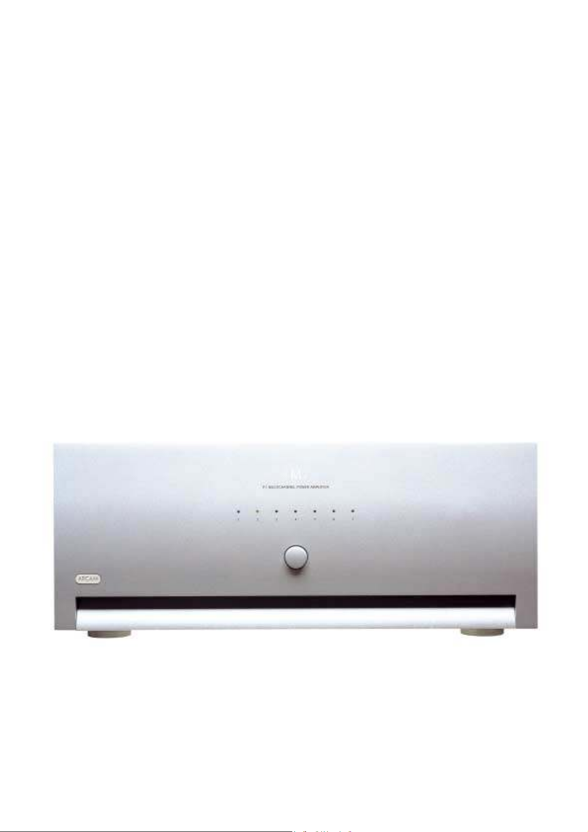
FMJ P7
7-Channel Amplifi er
P7
Issue 1.0
ARCAMARCAM
Page 2

Contents List
Section Issue
Technical specifications
! Technical specification -
! Rear panel silk screen -
Amplifier board L924
! Circuit description -
! Component overlay 1.0
! Parts list 1.1
! Circuit diagrams 1.1
Controller board L925
! Circuit description -
! Component overlay 1.0
! Parts list 1.2
! Circuit diagrams 1.2
Transformer specifications
! L911TX 1.0
! L912TX 1.0
! L920TX 1.0
! L921TX 1.0
Mechanical
! General assembly parts list -
! Assembly diagrams
Front panel TX tray - -
Rear panel Chassis -
Page 3

Technical
Specifications
Page 4

Technical Specifications
All measurements are with 230V/50Hz mains power
Continuous output power
All channels driven, 20Hz – 20Khz, 8 ohm 150W per channel 1.05kW total
All channels driven, 20Hz – 20kHz, 4 ohm 230W per channel 1.62kW total
One or two channels driven at 1kHz, 8 ohm 160W per channel
One or two channels driven at 1kHz, 4 ohm 250W per channel
One or two channels driven at 1kHz, 3.2 ohm 300W per channel
Peak output current capability 25A per channel
Total harmonic distortion
At any level up to rated power, into 4 or 8 ohms <0.05% (20Hz – 20kHz)
Typically <0.005% at 1kHz
Frequency response +-0.2dB (20Hz – 20 kHz)
-1dB at 1Hz and 100kHz
Residual hum and noise
Referenced to full power -122dB, 20Hz – 20kHz, unweighted
Voltage gain x 28.3 (1V input gives 100W/8 ohm output)
Input impedance 22k ohm in parallel with 470pF
Output impedance 50m Ohm at 20Hz, 1kHz
120m ohm at 20kHz
Power requirements 115V or 230VAC, 50/60Hz, 3kW maximum via heavy duty IEC mains inlet
A soft start system eliminates large inrush currents at switch on
Dimensions W430 x D450 x H180 mm
Weight 31kg (68 Ib) nett
35kg (77 Ib) packed
Page 5

NCN
7 RS BACK
POWER INLET
230V
~
50 – 60 Hz
3700 VA
MAX
6 R SURR 5 RIGHT 4 CENTRE 3 LEFT 2 L SURR 1LS BACK
CAUTION – SHOCK HAZARD, DO NOT OPEN.
ACHTUNG – VOR OEFFNEN DES GERAETES NETZSTECKER ZIEHEN
SERIAL No. LABEL
12V TRIGGER
IN
WARNING: THIS APPLIANCE MUST BE EARTHED.
OPERATION.
THIS P RODUCT IS CERTIFIE D BY THE MANUFACTURE R TO COMPLY WITH DHHS RULE 21 CF R
SUBPA RT J APPLICABLE AT THE DATE OF MANUFACTURE.
DESIGNED & MADE IN THE UK BY:
A & R CAMBRIDGE LTD, WATERBEACH,
CAMBRIDGE, CB5 9PB.
Page 6

Amplifier
Board
L924
Contents
!
Circuit description
!
Component overlay
!
Parts list
!
Circuit diagrams
Page 7

P7 Amplifier Module
Circuit Description
Refer to L924 circuit diagrams
Introduction
L924 is the power amplifier module for the P7 multichannel
amplifier. There are 7 identical modules in the P7. The circuit
design is based on the A85 / A32 output stage topology.
The main features of the amplifier module are as follows:
• Preset ‘THX’ gain (29dB closed loop gain). 0dBV input
signal corresponds to 100 watts into 8Ω output power
• Capable of producing 150 watts of sinusoidal output
power into an 8Ω resistive load (with greater than
250W into 3.2Ω subject to thermal dissipation limits)
• Relay coupled output for silent power on / off and load
protection
• Opto-isolated fault and control lines to the
microprocessor PCB (to avoid hum loops and
instability, to improve EMC performance and crosstalk)
• DC coupled signal path with integrating servo to
remove residual DC errors
• Instantaneous load protection
• Mono block design (each channel is electrically isolated
from all others and has independent power supply
windings on the mains transformer)
• Integrated modular heatsink for good thermal
performance and ease of assembly / servicing
• Low harmonic and intermodulation distortion
• Flat frequency response
• Fast (and symmetrical) slew rate
• High damping factor
• Unconditionally stable into loads of up to ±90° phase
angle
Sheet 1
The input to the amplifier is connected via SK103. The 2
phono sockets are connected in parallel to allow ‘daisychaining’ of amplifier modules. R104 provides a DC leakage
path to the chassis (i.e. mains power earth) to prevent small
transformer leakage currents causing the electrical 0V of the
amplifier to rise significantly above mains earth potential.
C104 provides an EMC coupling between the local input
ground and the chassis to reduce common mode RF noise.
Star point SP101 connects the differently named electrical 0V
nets at a single point. This is to ensure the correct wiring
topology of the ground connections on the printed circuit
board. SP101 provides a good common ground reference
point when making voltage measurements on the PCB. Note
that 0V_DIG is not connected to SP101, as this is the
microprocessor ground.
Relay RLY101 connects the output of the amplifier to the
load via socket SK105.
L101 and R103 form part of a ‘Zobel’ network to decouple
the load at high frequencies to ensure amplifier stability into
capacitive loads.
Note that signals 6 through 9 are open collector outputs,
active low, referred to 0V_DIG with no pull-up resistors.
This is because they are wire OR’d on the microprocessor
PCB (L925), where the pull-up resistors to +5V digital are
located.
The line ‘NFB’ provides for a portion of the negative feedback of the
amplifier to be taken on the load side of RLY101. The components
that allow for this (R236 thru R239) are not presently fitted, meaning
that RLY101 is not included in the feedback loop.
SK104 connects to the microcontroller PCB. Note that all signals on
this connector are electrically isolated from the amplifier circuit
itself, via either opto isolators or the relay coil of RLY101. The 10pin connector has the following signals:
SK104
Pin Type Name Description
1 GND 0V_DIG Microprocessor ground return
2 PSU +24V_DIG +24 volt digital power supply
3 MUTE Not used
4 I/P OUT_RLY Relay drive for the output relay
5 Not used
6 O/P THERMPR
OT
7 O/P VIPROT Open collector short circuit fault
8 O/P DCPROT Open collector DC fault signal
9 O/P FAULT Open collector overall fault signal
10 Not used
(referred to 0V_DIG only) for
relay coil RLY101
RLY101 (LOW = output relay
ON)
Open collector thermal fault signal
(LOW = FAULT)
signal (LOW = FAULT)
(LOW = FAULT)
(LOW = FAULT)
Sheet 2
Port INPUT connects the input of the amplifier, referred to 0V_SIG,
which is the precision signal ground reference.
Zener diodes DZ202 and DZ203 limit the input signal amplitude to
approximately 5.3Vpk. This is to prevent damage to the input of opamp IC200, due to a leaky source signal or electrostatic discharge.
R223, R228 and C210 form a passive 1
3dB corner frequency of roughly 330kHz to prevent ultrasonic
signals from entering the circuit and possibly causing damage.
The main amplifier circuit is a ‘classic’ current feedback design.
IC200A is configured as a non-inverting amplifier with a gain of 2.
Its purpose is to provide current outputs (via its power supply pins)
and a current input (via its output pin). This forms the voltage to
current (transimpedance) conversion and phase splitting necessary to
drive the voltage gain stage. The ‘current feedback’ occurs because
when IC200 drives its 44Ω load to ground, the power supply pin
currents are half-wave rectified versions of the drive current of the
amplifier. This causes voltage gain, which is buffered and passed on
to the outputs. The feedback from the output to pin 1 of IC200 acts to
reduce the gain of the amplifier; when this current is roughly equal to
the current required to drive the input signal into 44Ω, equilibrium is
reached and the closed loop gain is defined. The output stage
provides the vast majority of the current required to drive the 44Ω
signals to ground. The op-amp only provides a very small error
current sufficient to give the required voltage magnification.
Transistors TR204 and TR203 are wired as cascodes (common base
amplifiers). Their purpose is to provide IC200 with ±15V power
supply rails, whilst allowing IC200’s power supply pin currents to
pass through them to the NPN and PNP current mirrors.
The resistor, zener diode and capacitor circuits on the bases of TR204
and TR203 are to provide a controlled ramp up during power on, a
stable power supply voltage and good local HF decoupling.
st
order low pass filter with a –
Page 8

Transistors TR200, TR201 and TR202 form a PNP Wilson
current mirror. Likewise TR205, TR207 and TR206 form an
NPN Wilson current mirror. The outputs of these two current
mirrors are connected together via the bias network around
TR212.
The two current mirrors combine to provide a very high-gain
current to voltage (transresistance) gain stage, which provides
all the voltage gain of the amplifier (roughly 80dB at low
frequency).
C205, C207, R221 and R222 provide the loop compensation
for the amplifier. They combine to produce an open-loop pole
at roughly 10kHz and a corresponding open-loop zero around
500kHz. This allows for good time domain performance and
clean square wave reproduction. The amplifier is designed to
be critically damped. There should be no ringing or overshoot
apparent on the output signal when a (small) step function is
applied to the input.
Diodes D200 and D202 act to limit the current through
TR202 and TR206 in the event of a fault condition. When the
input current exceeds 14mA the diodes conduct and the
transresistance stage becomes a constant current source,
killing the open loop gain and preventing damage to the
transistors.
Resistors R219 and R220 decouple the supplies for the
amplifier gain stages from the main power rails. This is to
permit the bootstrap circuit to modulate these supplies,
increasing efficiency. The bootstrap will be described in more
detail later.
TR212 provides a 4.7V bias voltage to allow the following
pre-driver stage to operate in class ‘A’. It also acts as a V
BE
multiplier for TR209 and TR214 to maintain an
approximately constant current as the ambient temperature
inside the box changes.
TR209 and TR214 form a class ‘A’ pre-driver emitter
follower stage to boost the current gain and isolate the
transresistance stage from the output transistors. This is
important to keep the loop gain of the amplifier high and thus
minimise distortion. TR208 and TR213 act as a current limit
(roughly 30mA) to prevent the destruction of TR209 and
TR214 in a fault condition.
R247, R248, R249 and R250 are to loosely decouple the
emitters of TR209 and TR214 from the output stage. This is
very important. The output devices (Sanken power
Darlingtons) have inbuilt temperature compensating diodes
which control the bias voltage to their bases. Each output
device has a 150Ω resistor so that the inbuilt diodes can
accurately control quiescent V
and hence collector current
BE
as the output power and device temperature varies. Preset
potentiometer RV200 adjusts the quiescent current. NB:
Ensure that the amplifier has fully warmed up before
adjusting the quiescent current. D201 protects the output
devices from destruction in the event of the preset
potentiometer going open circuit. PL200 allows the test
engineer to measure the bias voltage (and thus collector
current).
C217, C218, C220 and C221 provide local HF stability
around the output transistors to prevent parasitic oscillation.
D204 and D205 are catch diodes to reduce the effects of
induced back-EMF in the loudspeaker load.
R254 and C223 form part of the ‘Zobel’ network that ensures
the amplifier sees a constant load of roughly 4.7Ω at very
high frequencies. This helps to improve stability and reduce
HF output noise.
C208 and C209 provide local high frequency decoupling for
the output devices.
IC200B forms the DC integrating servo. Its purpose is to remove
residual DC errors due to slight device mismatch and component
tolerances. It is configured as an inverting integrator with a time
constant of 0.47 seconds. Any positive DC offset at the output of the
amplifier will cause the output of the op-amp to go negative,
increasing the current in the negative supply pin and thus ‘pulling’
the output down to ground (and vice versa). D203 protects the
inverting input of IC200B in a fault condition.
The bootstrap circuit consists of C213, C214, R241, R242, R219 and
R220. The purpose of the bootstrap is to allow the output voltage
swing to modulate the power supply rails of the input and voltage
gain stages. This allows this circuit’s power supply voltage to exceed
the main power rails connected to the output devices, allowing the
driver stage to fully drive the output and thus give the best thermal
efficiency. The ‘bottom’ of R219 sees a peak-to-peak voltage swing
of approximately 15 volts at full output power (i.e. it goes 7.5 volts
above the rail at the peak of the cycle). The ‘top’ of R220 should see
the same voltage swing.
Sheet 3
This sheet contains the protection circuits and interface to the
microprocessor signals.
TR309, TR305 and their associated components form the
instantaneous load protection circuit for the output transistors. They
sense the voltage across the 0.22Ω emitter resistors (hence emitter
current) and the collector-emitter voltage, cutting off the base drive to
the output transistors when the collector current or device power
dissipation exceeds a preset limit.
The protection circuit is designed to allow large (unrestricted)
currents into loads of 3Ω and above but limit the current into a short
circuit or very low impedance load. C318, C319, R335 and R336
form a 2.2ms time constant, which will allow larger transients of
current delivery for a few milliseconds, to ensure that the amplifier
has a sufficiently large transient capability to drive ‘difficult’
loudspeaker loads with a music signal.
TR311 also turns on when the protection circuit activates. This
switches on optocoupler IC300B causing a fault signal to be
transmitted to the microcontroller. The microcontroller will then
switch off the output relay to protect the amplifier.
TR310, TR302 and their associated components form the DC offset
detection circuit. A positive DC offset at the output will turn on
TR310. A negative DC offset at the output will turn on TR302, thus
causing TR313 to turn on. In either case optocoupler IC300A is
switched on causing a fault signal to be transmitted to the
microcontroller. The microcontroller will then switch off the output
relay to protect the loudspeaker voice coils from overheating.
Thermistor TH300 is connected to the positive supply rail, adjacent to
the collector leg of one of the power output devices. This allows it to
sense the collector temperature of the output device. Its impedance
when cool is low, typically a few hundred ohms. In the event of a
thermal overload (above 110°C), TH300 will go to a high impedance
state. This will turn on TR301, which then turns on TR300, causing
optocoupler IC300D to switch on, sending a fault signal to the
microcontroller. The microcontroller will then switch off the output
relay until such time as the unit has cooled down to an acceptable
level (80°C or so). TR301 is configured with a small amount of
hysterisis (positive feedback) to ensure a clean signal is transmitted to
the microprocessor via IC300D.
Optocoupler IC300C is connected in series with the 3 optocouplers
mentioned above, producing an overall fault signal. This is so that the
microcontroller can determine in which module the fault has
occurred, permitting selective control of the output relay for each
module in the amplifier.
Page 9

Page 10

L924 Amplifier Module Parts List Issue 1.1
Designator Part Description
BR300 3BGBU8D Diode Bridge Rectifier GBU8D Plastic Package 8A 200V
BR301 3BGBU8D Diode Bridge Rectifier GBU8D Plastic Package 8A 200V
C103 2C410 Capacitor SM 1206 X7R Ceramic 50V 10% 100N
C104 2C210 Capacitor SM 1206 NPO Ceramic 50V 5% 1N0
C200 2C410 Capacitor SM 1206 X7R Ceramic 50V 10% 100N
C201 2C410 Capacitor SM 1206 X7R Ceramic 50V 10% 100N
C202 2C410 Capacitor SM 1206 X7R Ceramic 50V 10% 100N
C203 2N710 Capacitor Radial Electrolytic Dia 5mm Pitch 5mm 100UF 25V
C204 2N710 Capacitor Radial Electrolytic Dia 5mm Pitch 5mm 100UF 25V
C205 2D110W2 Capacitor Boxed Polyprop 5mm Pitch 250V 5% 100P
C207 2D110W2 Capacitor Boxed Polyprop 5mm Pitch 250V 5% 100P
C208 2C410A Capacitor SM 1812 X7R Ceramic 500V 10% 100N
C209 2C410A Capacitor SM 1812 X7R Ceramic 500V 10% 100N
C210 2D147W Capacitor Boxed Polyprop 5mm Pitch 100V 5% 470P
C212 2K447 Capacitor Boxed Polyester 5mm Pitch 10% 63V 470N
C213 2N710B Capacitor Radial Electrolytic Dia 10mm Pitch 5mm 100UF 100V
C214 2N710B Capacitor Radial Electrolytic Dia 10mm Pitch 5mm 100UF 100V
C215 2N610 Capacitor Radial Electrolytic Dia 5mm Pitch 5mm 10UF 50V
C216 2N610 Capacitor Radial Electrolytic Dia 5mm Pitch 5mm 10UF 50V
C217 2C047B Capacitor SM 0805 NPO Ceramic 200V 5% 47PF
C218 2C047B Capacitor SM 0805 NPO Ceramic 200V 5% 47PF
C220 2C047B Capacitor SM 0805 NPO Ceramic 200V 5% 47PF
C221 2C047B Capacitor SM 0805 NPO Ceramic 200V 5% 47PF
C223 2K347 Capacitor Boxed Polyester 5mm Pitch 10% 63V 47N
C225 2N610 Capacitor Radial Electrolytic Dia 5mm Pitch 5mm 10UF 50V
C300 2C410 Capacitor SM 1206 X7R Ceramic 50V 10% 100N
C301 2N710 Capacitor Radial Electrolytic Dia 5mm Pitch 5mm 100UF 25V
C305 2C410 Capacitor SM 1206 X7R Ceramic 50V 10% 100N
C306 2C410 Capacitor SM 1206 X7R Ceramic 50V 10% 100N
C318 2N710 Capacitor Radial Electrolytic Dia 5mm Pitch 5mm 100UF 25V
C319 2N710 Capacitor Radial Electrolytic Dia 5mm Pitch 5mm 100UF 25V
C320 2V710 Capacitor Non-Polar Radial Electrolytic 100UF 16V
C321 2V710 Capacitor Non-Polar Radial Electrolytic 100UF 16V
C322 2P910AM Capacitor Radial Electrolytic Dia 40mm PCB Mount 10000uF 71V
C323 2P910AM Capacitor Radial Electrolytic Dia 40mm PCB Mount 10000uF 71V
D101 3AS16W Diode Surface Mount Small Signal BAS16W SOT-23 Package
D200 3AS16W Diode Surface Mount Small Signal BAS16W SOT-23 Package
D201 3AS16W Diode Surface Mount Small Signal BAS16W SOT-23 Package
D202 3AS16W Diode Surface Mount Small Signal BAS16W SOT-23 Package
D203 3AV99W Diode Dual Surface Mount Small Signal BAV99 SOT-23 Package
D204 3B4003 Diode 1N4003 DO-41 Package
D205 3B4003 Diode 1N4003 DO-41 Package
D300 3AS16W Diode Surface Mount Small Signal BAS16W SOT-23 Package
D301 3CW315V Zener Diode 0.25W Surface Mount BZX84C15V SOT-23 Package
D303 3AS16W Diode Surface Mount Small Signal BAS16W SOT-23 Package
D307 3AS16W Diode Surface Mount Small Signal BAS16W SOT-23 Package
D308 3CW322V
D309 3CW322V
DZ200 3CW315V Zener Diode 0.25W Surface Mount BZX84C15V SOT-23 Package
DZ201 3CW315V Zener Diode 0.25W Surface Mount BZX84C15V SOT-23 Package
DZ202 3CW34V7 Zener Diode 0.25W Surface Mount BZX84C4V7 SOT-23 Package
DZ203 3CW34V7 Zener Diode 0.25W Surface Mount BZX84C4V7 SOT-23 Package
IC200 5B072D Opamp TL072CD SO-8 Package
IC300 5T3Q66 Opto Isolator Quad PC3Q66Q
L101 7D002C Inductor AC 2u2 SELF BONDED
PL100 8K6201 CON SINGLE ROW HDR 0.1IN VERTICAL 2WAY
PL200 8K6201 CON SINGLE ROW HDR 0.1IN VERTICAL 2WAY
R103 1H822 Resistor Metal Film 0.25W 1% 2R2
R104 1A110 Resistor 1206 Surface Mount 0.25W 1% 100R
R207 1A110 Resistor 1206 Surface Mount 0.25W 1% 100R
R208 1A110 Resistor 1206 Surface Mount 0.25W 1% 100R
R210 1A327 Resistor 1206 Surface Mount 0.25W 1% 27K
Page 11

L924 Amplifier Module Parts List Issue 1.1
Designator Part Description
R211 1A327 Resistor 1206 Surface Mount 0.25W 1% 27K
R212 1A327 Resistor 1206 Surface Mount 0.25W 1% 27K
R213 1A327 Resistor 1206 Surface Mount 0.25W 1% 27K
R214 1A047 Resistor 1206 Surface Mount 0.25W 1% 47R
R216 1A047 Resistor 1206 Surface Mount 0.25W 1% 47R
R217 1A047 Resistor 1206 Surface Mount 0.25W 1% 47R
R218 1A047 Resistor 1206 Surface Mount 0.25W 1% 47R
R219 1H122 Resistor Metal Film 0.25W 1% 220R
R220 1H122 Resistor Metal Film 0.25W 1% 220R
R221 1A233 Resistor 1206 Surface Mount 0.25W 1% 3K3
R222 1A233 Resistor 1206 Surface Mount 0.25W 1% 3K3
R223 1A210 Resistor 1206 Surface Mount 0.25W 1% 1K0
R224 1A210 Resistor 1206 Surface Mount 0.25W 1% 1K0
R225 1A210 Resistor 1206 Surface Mount 0.25W 1% 1K0
R226 1A210 Resistor 1206 Surface Mount 0.25W 1% 1K0
R227 1A210 Resistor 1206 Surface Mount 0.25W 1% 1K0
R228 1A322 Resistor 1206 Surface Mount 0.25W 1% 22K
R229 1H022 Resistor Metal Film 0.25W 1% 22R
R230 1H022 Resistor Metal Film 0.25W 1% 22R
R231 1A247 Resistor 1206 Surface Mount 0.25W 1% 4K7
R232 1H156 Resistor Metal Film 0.25W 1% 560R
R233 1H156 Resistor Metal Film 0.25W 1% 560R
R234 1H168 Resistor Metal Film 0.25W 1% 680R
R235 1H168 Resistor Metal Film 0.25W 1% 680R
R236 1H239 Resistor Metal Film 0.25W 1% 3K9
R237 1H239 Resistor Metal Film 0.25W 1% 3K9
R238 1H239 Resistor Metal Film 0.25W 1% 3K9
R239 1H239 Resistor Metal Film 0.25W 1% 3K9
R240 1A510 Resistor 1206 Surface Mount 0.25W 1% 1M0
R241 1C210 Resistor Carbon Film 2W 5% 1K0
R242 1C210 Resistor Carbon Film 2W 5% 1K0
R245 1A022 Resistor 1206 Surface Mount 0.25W 1% 22R
R246 1A022 Resistor 1206 Surface Mount 0.25W 1% 22R
R247 1A115 Resistor 1206 Surface Mount 0.25W 1% 150R
R248 1A115 Resistor 1206 Surface Mount 0.25W 1% 150R
R249 1A115 Resistor 1206 Surface Mount 0.25W 1% 150R
R250 1A115 Resistor 1206 Surface Mount 0.25W 1% 150R
R254 1D847 Resistor Carbon Film 0W5 5% 4R7
R255 1A268 Resistor 1206 Surface Mount 0.25W 1% 6K8
R257 1A210 Resistor 1206 Surface Mount 0.25W 1% 1K0
R300 1A110 Resistor 1206 Surface Mount 0.25W 1% 100R
R301 1A110 Resistor 1206 Surface Mount 0.25W 1% 100R
R302 1A110 Resistor 1206 Surface Mount 0.25W 1% 100R
R303 1A322 Resistor 1206 Surface Mount 0.25W 1% 22K
R304 1A127 Resistor 1206 Surface Mount 0.25W 1% 270R
R305 1A310 Resistor 1206 Surface Mount 0.25W 1% 10K
R306 1A310 Resistor 1206 Surface Mount 0.25W 1% 10K
R307 1A339 Resistor 1206 Surface Mount 0.25W 1% 39K
R310 1A110 Resistor 1206 Surface Mount 0.25W 1% 100R
R311 1A110 Resistor 1206 Surface Mount 0.25W 1% 100R
R314 1A110 Resistor 1206 Surface Mount 0.25W 1% 100R
R315 1A110 Resistor 1206 Surface Mount 0.25W 1% 100R
R316 1A322 Resistor 1206 Surface Mount 0.25W 1% 22K
R320 1A322 Resistor 1206 Surface Mount 0.25W 1% 22K
R321 1A322 Resistor 1206 Surface Mount 0.25W 1% 22K
R332 1A322 Resistor 1206 Surface Mount 0.25W 1% 22K
R333 1A322 Resistor 1206 Surface Mount 0.25W 1% 22K
R334 1A247 Resistor 1206 Surface Mount 0.25W 1% 4K7
R335 1A022 Resistor 1206 Surface Mount 0.25W 1% 22R
R336 1A022 Resistor 1206 Surface Mount 0.25W 1% 22R
R337 1A210 Resistor 1206 Surface Mount 0.25W 1% 1K0
R338 1A133 Resistor 1206 Surface Mount 0.25W 1% 330R
Page 12

L924 Amplifier Module Parts List Issue 1.1
Designator Part Description
R339 1A133 Resistor 1206 Surface Mount 0.25W 1% 330R
R340 1A310 Resistor 1206 Surface Mount 0.25W 1% 10K
R341 1A310 Resistor 1206 Surface Mount 0.25W 1% 10K
R342 1A412 Resistor 1206 Surface Mount 0.25W 1% 120K
R343 1A410 Resistor 1206 Surface Mount 0.25W 1% 100K
RLY101 A220 Relay 1P2T 24V
RV200 6F110V Preset Vertical Mount 100R linear
SK103 8D226 Phono socket 2 way vertical gold
SK104 8K2810 CON HORIZ PCB SKT 10WAY
SK105 8D421 Connector 4mm 2 way horizontal
SK300 8K2302 CON MINIFIT HCS V 2WAY
SK301 8K2302 CON MINIFIT HCS V 2WAY
TH300 1T007 Thermistor PTC SM 110 degrees C
TR200 4AFMMT597 Transistor FMMT597 SOT23 Package
TR201 4AFMMT597 Transistor FMMT597 SOT23 Package
TR202 4B1740 Transistor 2SA1740 SOT-89 Package
TR203 4AFMMT597 Transistor FMMT597 SOT23 Package
TR204 4AFMMT497 Transistor FMMT497 SOT23 Package
TR205 4AFMMT497 Transistor FMMT497 SOT23 Package
TR206 4B4548 Transistor 2SC4548 SOT-89
TR207 4AFMMT497 Transistor FMMT497 SOT23 Package
TR208 4AFMMT497 Transistor FMMT497 SOT23 Package
TR209 4B4548 Transistor 2SC4548 SOT-89
TR210 4CSAP15N Transistor SAP15NY
TR211 4CSAP15N Transistor SAP15NY
TR212 4AFMMT497 Transistor FMMT497 SOT23 Package
TR213 4AFMMT597 Transistor FMMT597 SOT23 Package
TR214 4B1740 Transistor 2SA1740 SOT-89 Package
TR215 4CSAP15P Transistor SAP15PY
TR216 4CSAP15P Transistor SAP15PY
TR300 4AFMMT497 Transistor FMMT497 SOT23 Package
TR301 4AFMMT597 Transistor FMMT597 SOT23 Package
TR302 4AFMMT597 Transistor FMMT597 SOT23 Package
TR305 4AFMMT597 Transistor FMMT597 SOT23 Package
TR309 4AFMMT497 Transistor FMMT497 SOT23 Package
TR310 4AFMMT497 Transistor FMMT497 SOT23 Package
TR311 4AFMMT497 Transistor FMMT497 SOT23 Package
TR312 4AFMMT497 Transistor FMMT497 SOT23 Package
TR313 4AFMMT497 Transistor FMMT497 SOT23 Package
Z100 L924PB BLANK PCB 7 CHANNEL AMP MODULE
Z101 E107AY ASSEMBLY OF REAR PANEL MODULE AND SILK SCREEN
Z102 E915HK Finished Heatsink for single channel amp module
Z103 HF4V09B SCREW SELF-TAPPING-SEMS NO.4 X 9MM PAN TORX-SLOT STEEL ZINC-PLATE BLK
Z104 HF4V09B SCREW SELF-TAPPING-SEMS NO.4 X 9MM PAN TORX-SLOT STEEL ZINC-PLATE BLK
Z105 HF4V09B SCREW SELF-TAPPING-SEMS NO.4 X 9MM PAN TORX-SLOT STEEL ZINC-PLATE BLK
Z106 E950MC INSULATOR P7 TRANSISTOR INSULATING PAD
Z107 HB3B12A SCREW TAPTITE HEXAGON WASHER FACE M3X12MM
Z108 HB3B12A SCREW TAPTITE HEXAGON WASHER FACE M3X12MM
Z109 HB3B12A SCREW TAPTITE HEXAGON WASHER FACE M3X12MM
Z110 HB3B12A SCREW TAPTITE HEXAGON WASHER FACE M3X12MM
Page 13

C104
1N0 SM
0V_SIG
R104
100R SM
EMC
Inputs
SK103
PHONO2G
1
TP100
F
N
TP101
PL100
1
2
2WVERTJUMPER
To microprocessor PCB
+24V_DIG
1
2
MUTE
3
OUT RLY
4
5
THERMPROT
6
7
VIPROT
DCPROT
8
FAULT
9
10
VIPROT
DC
THERM
FAULT
BASE1
BASE2
L924C2
L924C2_1.1.sch
INPUT
BASE1
BASE2
NFB
NB: Signals THERMPROT, VIPROT,
DCPROT and FAULT are open
collector outputs, active low,
referenced to 0V_DIG with no pull up
resistors
EMITTER1
EMITTER2
OUTPUT
SK104
10WAY-H-0.1-F
Microprocessor GND
Microprocessor +24V
MUTE not used
Output relay control
Not used
Thermal protection
SOA protection
DC offset protection
Overall fault signal
Not used
L924C3
L924C3_1.1.sch
EMITTER1
EMITTER2
OUTPUT
Amplifier circuit Protection and supplies
TP102
VIPROT
DCPROT
THERMPROT
FAULT
NB: Nets +24V_DIG and 0V_DIG are isolated from amplifier circuit
+24V_DIG
TP103
TP104
TP105
TP106
TP107
TP108
TP109
0V_DIG
RLY G2R-1E-24DC 16A SPDT
OUT RLY
RLY101A
RLY G2R-1E-24DC 16A SPDT
TP110
RLY101B
C103
100N SM
R103
2R2 MF
L101
2U2 AIR CORED
D101
BAS16W SM
Electrical ground star point
0V_HF
0V_PSU
TP111
SK105
0V_SIG
SP101
STAR_8
0V_LS0V_ZOB
Z100
PCB HEATSINK
L924PB
Z101
SUB PANEL
E107AY
Z102
E915HK
Z103
SUB PANEL SUB PANEL SUB PANEL
SCREW SCREW SCREW
HF4V09B
Z106
TRANSISTOR
INSULATOR
E950MC
Z104
HF4V09B
Z107
M3 TAPTITE M3 TAPTITE M3 TAPTITE M3 TAPTITE
HB3B12A
Z105
HF4V09B
Z108
HB3B12A
Z109
HB3B12A
Z110
HB3B12A
NB: Feedback around relay not fitted
4MM 2W HOR
TP112
0V_LS
DRAWING TITLE
A & R Cambridge Ltd.
Pembroke Avenue
Waterbeach
Cambridge CB5 9PB
P7 Amplifier Module
L924C1_1.1.sch
Filename:
Notes:
Contact Engineer:
02_E055 JR 4/3/2002 FIXED DC FAULT AT POWER ON SEQUENCE BY FEEDBACK 1.1
INITIALS
Contact Tel: (01223) 203200Jonny Reckless
ECO No.
Printed:
DATE
7-Mar-2002
DESCRIPTION OF CHANGE
1 3Sheet of
DRAWING NO.
L924CT
ISSUE
 Loading...