

Page 1

Service Manual
ARCAM
A65/75
Issue 1.0
DiVA A65, A75 & P75 Plus
Amplifi ers
ARCAM
Page 2

Contents List
!
Contents list
!
Circuit description
!
Service guide
!
Circuit diagrams
!
Component overlays
!
Circuit board parts list
!
General assembly parts list
Page 3

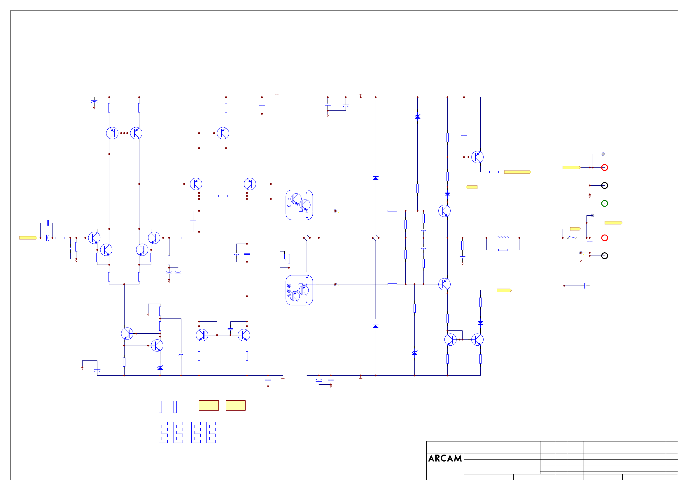
A65/75/75P Plus Circuit Description
PSU
In order get the output devices to tu rn fully on and achieve the
greatest efficiency, an auxiliary rail is formed from a charge pump
driven by the main AC outputs from the transformer. C304,305 &
D301,302 charge on alternate cycles. In th e other cycle the charge
on C304,305 is pu mped into C310,311 respectively. Thi s creates a
voltage much greater than the standard rails, but wi th low regulation
and high ripple. This is then regulated to 38V via emitter followers
Q300,302,303,305 from a zener stabilized voltage (D304,305)
The Pre-amp ±15V supply comes from linear regulators Z300,301.
The transformer is a dual voltage unit, the required voltage being
selected b y which fuse holder is fitted with the appropriat e fuse. If an
alternative to 115V or 230V is requ ired then a different transformer
is fitted. Th e secondary is centre tapped for the main rails, but a
separate winding is added for the uC supply.
The star ground p oint SP300 is not a component on the PCB and is
on the schematic only for layout purposes.
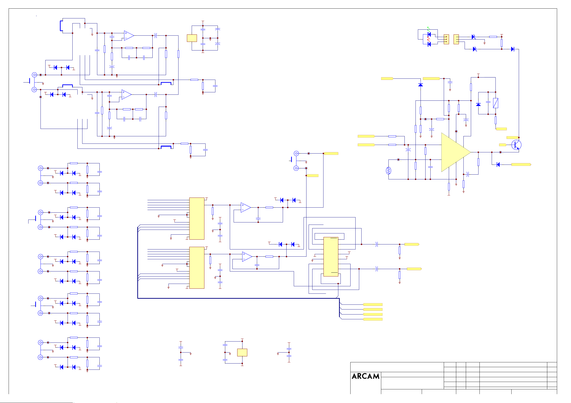
Pre-amp
The direct signal path (line in, tone controls defeated) consists of a
single op-amp gain stage, buffering the j-fet input multiplexers and
Tape Monitor and AV switches . The selected input is AC coupled to
the op-amp, the output is DC to the Pre-out, via a j- f et "pre-mute"
switch. This switch is controlled by the uC in such a way that when
ever the output relay changes state signal is removed from the power
amplifier (A65/75).
The MM phono stage (by passable A75 only, SW100) is opamp
based. The circuit is AC coupled to give RIAA/IEC low frequency
response. The c artridge is loaded by R100,101,C119,120. The 1kHz
gain is 56dB, and RIAA eq set by
R110,112,111,113,C127,129,128,130.
Each line input has static protection a ffor ded by the ba ck to back
diodes (e.g. D101,103), and RF filtering is set by R118,C134 etc.
The selected input is buffered for Tap e output by Z104 set as a
follower. The output resistor is inside the feedback loop so to keep
the output impedance low and short protection is catered for.
C121,122 maintain stabilit y i nto capacitive loads.
From the tape monitor switch (Z105) onwards the signal is AC
coupled (C151,152). From there the signal is fed to the tone controls.
These consist of two stages: Balance and buffer (Z160), and
Bass/Treble Z161. The output of this stage is again AC coupled.
Switch SW162 selects whether the tone adjusted signal or a direct
signal reaches the gain section. In the A75 Z164 can be used to
bypass the volu me control when AV input is selected. This fixes th e
gain to allow an external AV processor to control the volume setting.
The gain stage (Z163) has a gain of 2.2, and the same low impedance
output arrangement as the Tape output. The signal from this stage to
the Pre- amp outputs and the Power amp input is controlled by a
pre-mute (Z171). This removes thumps and clicks, and in the case of
the Power amp r elay changing state, removes signal so ar cing will
not take place.
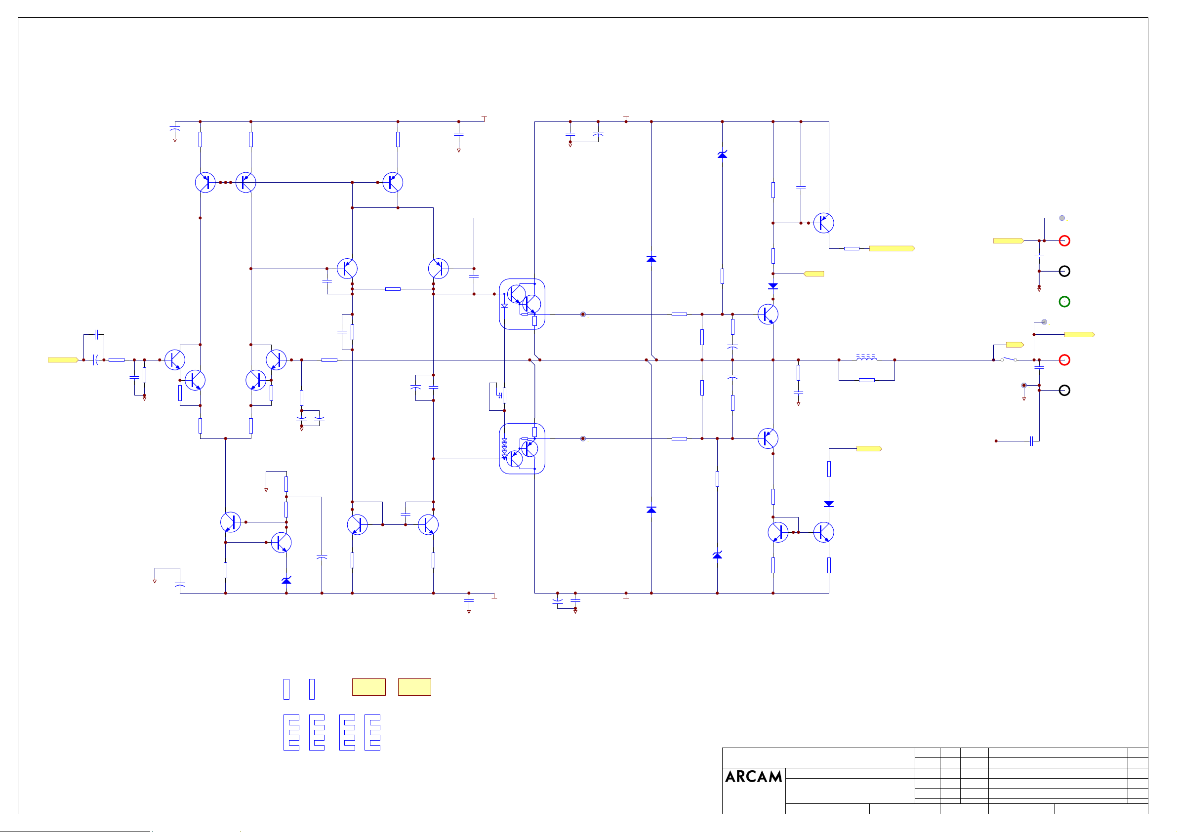
Power Amplifier
The new topology is a high gain voltage feedback design, with a
bipolar output stage. Its signal path is designed to be fully
symmetrical, despite not having a symmetrical circuit (symmetrical
rail to rail). This is achieved with a new dual differential input gain
block, where the input differential sees a symmetrical active load
(Q600,601,700,701) before driving the second voltage amplification
stage (VAS) differential (Q603,604,703,704). This could be
described as two Wilson mirrors with their bases clamped together.
The second differential also has an active load of a more traditional
mirror (Q610,611,710,711), and this gives a push pull signal to the
input of the output stage, improving on the traditional single ended
current source of the often called "blameless" topology.
The input pair (Q60 6,607,618,619, 706,707,718,719 ) are in a
Darlington confi guration to lower input current offset which in turn
will lower DC offset at the output, as the impeda nces seen on the
input nodes are necessarily high for the wide bandwidth required.
The output stage is a simple bipola r darlington (Q614,615,714,715).
However, the devices used are Darlingt on devices with integral
diodes. This means the bias temperature compensation i s part of the
output device enabling smaller number of devices, no extra devices
on the heatsink (vital for this mechanical layout) and more consistent
temperature compensation of bias. Also the resi st ors are also
integral, saving a large amount of PCB real estate and hand insertion
cost, while also able to be used as bias set test points and protection
sensing.
Due to the dec reased efficiency of this type of output stage over the
previous bootstrapped Mosfet output, a separate set of rails is
required for the VAS stage in order to satu rate the output transistors.
The operation of this is outlined in the Power supply section.
However, these rails are individually regulated for each channel to
decrease power supply crosstalk.
The protecti on of the output stage is taken care of by a proprietary IC
(Z101). This takes care of the switch on delay (R150,C149), DC
offset (R102,103,C147), Thermal trip (TH100), and safe operating
area.
The safe op erating area is monitored by a network which
compensates for the voltage across the output devices , current
through them, and duration of power (R627,606,625,605,C617 &
symmetrical associated components) and this is sent to the protection
IC via (Q605,612,613,616,617,712,713,716,717).
The output of the protection IC is sent to the micro controller (uC) to
signal the output relay (RLY1) status. Also, for output muti ng
purposes, the uC can switch the relay via Q100.
Input Selection
The uC cont r o ls the operation of the unit. IR commands are received
from RX900 on a break-off PCB found on the front panel and fed via
LK900/LK903 3-way ribbon. On power on/off the current state of
the pre-amp switching stored in an EEPR O M Z906. The inp ut
switching is 5V logic level and is direct from the uC to the DPDT
analogue switches in the case of Tape Monito r ( Z105), AV
(Z164,A75 on ly), Pre-mute (Z171) and Mute Q100. The source
selector is achieved by 8 way analogue multiplexors (Z102,103) and
the control signals are decoded from the uC from MUX1,2,3 by
Z907 which also drives the appropriate front panel LED. The input
selection is set by the remote control or the rotary encoder on the
front panel display PCB. Tape monitor and AV mode(A75 only) is
set by SW900.
Volume Control
The volume control is a motorized manual type, where the signals
are routed through the 8-way ribbon LK189. The motor drive comes
from Z905, which is a logic level controllable motor driver. It has its
own unregulated PSU (D907,C920),an d the speed of the volume
knob is dictated by the REF pin. The circuit (Q900,R905,901,C901)
allows the speed to vary from just ab ove stall to full as the volume
control button is depressed on the remote.
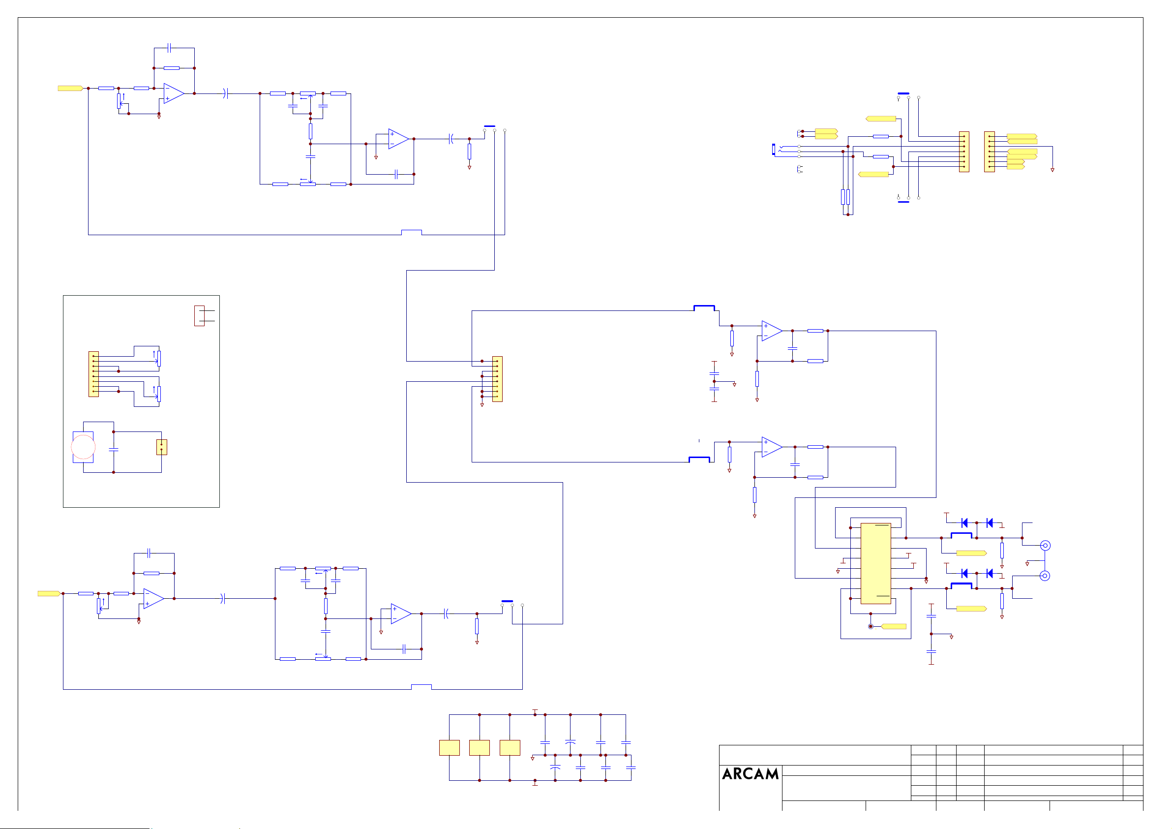
SIM Module
The connector PL161 (P75 only) allows the fitting of the ARCAM
SIM module. In order to allow this to operate LK172 & LK173 must
be removed. This will allow 12V trigger signals to operate the P75.
Headphones
The Speaker outputs (SK600,700) are connected to the headphone
socket (SK162) via an 8-way ribbon LK170,171. The output is
attenuated by a resistor network R161,162,236,237. The Relay drive
is fed through the headphone socket's switch (HPSW1,2) so that
when headphones are inserted the speakers are disconnected. Switch
SW163 allows the separate switching of the second speaker
terminals on SK600,700.
Page 4

A65, A75 & P75 Service Guide
Fault diagnostics
Fault Action
No power Check mains fuse
Stuck in protection Check power supply rails
Intermittent audio on one channel Check for dry joints around o/p
Fails to respond to commands Check supply to remote circuit
Volume control rubs on front panel Pull knob out from fascia
Audio crackles on o/p Check for component break down
Power supply test points
Position Voltage
LK125 +37 volts DC
LK126 -37 volts DC
LK271 or black speaker terminal 0 volts
LK303 +15 volts DC
LK301 - 15 volts DC
Q300 emitter +38 volts DC
Q304 emitter +38 volts DC
Q302 emitter -38 volts DC
Q305 emitter -38 volts DC
D910 emitter +5 volts DC remote supply
IQ settings
Model IQ setting Comments - (22/01/02)
A65 37mV
A75 37mV
P75 37mV
A85 12mV Set for 8.5mV cold, reset for 12mV when warm
P85 12mV Set for 8.5mV cold, reset for 12mV when warm
A65 plus 12 to 15mV
A75 plus 12 to 15mV
P75 plus 12 to 15mV
!
To isolate a fault between pre and power stage remove C602 (left channel) or C702 (right
channel).
!
Always check and re-solder o/p device SAP15N and SAP15P pin connections.
!
Replace Z900 IC if software version is below version 3 ( note version 82 is also ok ).
!
Make sure R127 is not touching LK130.
!
When replacing the top cover with a new top it may be necessary to re-drill the fixing holes.
Check transformer connections
Check power supply rails
Check protection circuit voltages
Check for dry joints on o/p devices
devices
Check IC Z900
Check remote flex foil cable
Check for dry joints on selector pcb
using hot air gun & freezer spray
Check transformer connections
Hints & tips
Page 5

PHONO & INPUTS
L942C3_1.0.SCH
ACSENSE
PROT_OP_L
PROT_OP_R
PROTECTION MUTE
TAPECONTROL
MUX2
MUX3
PROT SENSE
SELOPL
SELOPR
HPSW2
TAPOL
TAPOR
MUX1
HPSW1
REMOTE CONTROL
L942C7_1.0.SCH
MUTE
MUX1
MUX2
MUX3
PROT SENSE
TONE CONTROL
L942C4_1.0.SCH
AVCONTROL
PREMUTE
TAPECONTROL
SELOPL
SELOPR
HPSW2
HPSW1
PREMUTE
ACLT1
PROT_OP_R
PROT_OP_L
PWRLEFT
PWRRIGHT
TAPOL
TAPOR
SP2_SEND_L
SP2_RETN_L
OP_L
OP_R
SP2_SEND_R
SP2_RETN_R
AVCONTROL
LEFT CHANNEL
L942C5_1.0.SCH
SP2_SEND_L
SP2_RETN_L
PWRLEFT
RIGHT CHANNEL
L942C6_1.0.SCH
PWRRIGHT
SP2_SEND_R
SP2_RETN_R
PROTECTION
OP_L
A1
A1
OP_R
A1
A1
POWER SUPPLY
L942C2_1.0.SCH
ACLT1
ACSENSE
USE 'exlude A65' FILTER FOR BOM
DRAWING TITLE
A & R Cambridge Ltd.
Pembroke Avenue
Waterbeach
Cambridge CB5 9PB
A65 PLUS AMP
Filename:
L942C1_1.0.PRJ
Notes:
TOP SHEET FOR A65 L942AY
Contact Engineer:
01_E020
Contact Tel: (01223) 203 200Travis Pierce
ECO No. DESCRIPTION OF CHANGE
TGP 12/12/01 PRODUCTION RELEASE 1.0
DATE
INITIALS
11-Dec-2001
Printed:
1 7Sheet of
DRAWING NO.
L942C1
ISSUE
Page 6
C600
100U EL 100V
0V_HF
+38V_L
+
R601
100R MF
R602
100R MF
R615
47R MF
0V_HF
C613
100N PE 100V
C614
100N PE 100V
0V_HF
+37V
+
C603
100U 50V YXF LOW Z
D601
ZENER 400MW 27V
PWRLEFT
C623
100N PE 100V
C602
+
22U SILMIC 2
R600
1K0 MF
C603
100P PPW
0V_SIG
R612
100K MF
0V_HF
R632
12K MF
Q600
BC556B
Q619
BC546B
+
C601
100U EL 100V
Q606
BC546B
R613
47R MF
Q607
BC546B
R617
680R MF
Q608
BC546B
Q601
BC556B
R614
47R MF
0V_HF
Q618
BC546B
R633
12K MF
C605
100U SILMIC 2
0V_SIG
R618
10K MF
R619
10K MF
Q609
BC546B
D600
4V7 400MW
C604
100P PPW
C610
100N PE 100V
R616
2K7 MF
+
R611
100K MF
+
C624
100U 25V ZA EL
Q611
2SC2240GR
+
C616
10U EL
Q604
2SA970GR
R620
10K MF
R603
100R MF
R634
470K MF
C625
10U EL
C607 100P PPW
Q602
BC556B
Q603
2SA970GR
+
C611
100N PE 100V
Q610
2SC2240GR
R604
100R MF
C612
100N PE 100V
RV600
220R PSET
0V_HF
C608
100P PPW
-38V_L
Q614
SAP15N
Q615
SAP15P
C626
100U 50V YXF LOW Z
Bias-L +
SET BIAS TO 12mV
Bias-L -
C615
+
100N PE 100V
0V_HF
-37V
D603
1N4003F
D604
1N4003F
R627
430R MF
R628
430R MF
R606
100R MF
R607
100R MF
R625
6K8 MF
R605
100R MF
C617
+
10U EL
+
C618
10U EL
R608
100R MF
R626
6K8 MF
D602
ZENER 400MW 27V
Q613
BC546B
R621
680R MF
R622
10K MF
D605
1N4148
Q612
2SC2240GR
0V_LS_L
Q616
2SA970GR
R624
10K MF
R609
100R MF
C609
22N CD
A1
R630
4R7 W2 CF
C619
100N PE 100V
Q605
BC556B
R623
10K MF
D606
1N4148
Q617
ZTX653
R610
100R MF
R629
47K MF
PROTECTION
L600
2U2H LAC SMALL
R631
2R2 CF
A1
SP2_RETN_L
470P CD
OP_L
RLY1A
RLY G5Z-2A-E
SPLE600
PD6
C620
0V_LS_L
0V_LS_L
C622
1N0 CD
SPLD600
C621
470P CD
SPLS600
Bot+
SK600B
SPKSKT_G
Bot-
SK600C
CHASS
SPKSKT_G
SP2_SEND_L
Top+
SK600A
SPKSKT_G
Top-
CL600
E856MC
HS600
E81801-75
CL601
E856MC
HS601
E81801-75
SP600
Q2-PAD-SAP
HS602
E81801-75
21mm x 32mm
SELF ADHESIVE
Q2 PAD
E852MC
HS603
E81801-75
SP601
21mm x 32mm
SELF ADHESIVE
Q2 PAD
E852MC
Q2-PAD-SAP
USE 'exlude A65' FILTER FOR BOM
DRAWING TITLE
A & R Cambridge Ltd.
Pembroke Avenue
Waterbeach
Cambridge CB5 9PB
A65 PLUS AMP
Filename:
L942C5_1.0.SCH
Notes:
Left Channel Power Amplifier
Contact Engineer:
01_E020
Contact Tel: (01223) 203 200Travis Pierce
ECO No. DESCRIPTION OF CHANGE
TGP 12/12/01 PRODUCTION RELEASE 1.0
DATE
INITIALS
11-Dec-2001
Printed:
5 7Sheet of
DRAWING NO.
L942C5
ISSUE
Page 7

REPLACE WITH IDENTICAL PART
ACLT1
R900
1R0 FU
MOTE900
C900
10N CD
0V_DIG
D906
1N4003F
R903
100R MF
R902
+
C914
100R MF
220U EL
0V_DIG
RX900
PIC-26043TM2
3
2
O/P
+5V
O/P
GND1Case
Case
GND +5V
REMOTE SENSOR SNAP OFF BOARD
IR RX
SUPPORT PAD
SP1
IR RX SUPPORT PAD
R901
12K MF
R904
10R MF
D908
ZENER 5V1 400MW
LK900
1
2
3
L856CA
+5v
R905
33K MF
+
C901
100U EL
0V_DIG
+5v
+
C915
100U EL
3WAY CABLE HOLDER
D907
1N4003F
LK903
+5V
Q900
BC556B
1
2
3
P900
REMO900
0V_DIG
C912
10N CD
3
5
4
6
9
0V_DIG
+5V
C916
100N CD
0V_DIG
PROT SENSE
CC1
MC1
REF
MC2
CC2
Z900
1
2
3
4
5
6
7
8
9
10
11
12
13
14
PB5
PB4
PA3
PA2
PA1
PA0
PB3
PB2
PB1
PB0
VSS
(TMR)/INT
PC0
PC1
+5V
Z905
8
BA6109
VCC17VCC2
VOLUME DRIVEMOTOR DRIVER
28
PB6
27
PB7
26
PA4
25
PA5
24
PA6
23
PA7
22
OSC2
21
OSC1
20
VDD
19
RES
HT48R30 28-DIP-B-0
18
PC5
17
PC4
16
PC3
15
PC2
R913
10K MF
5
6WP7
SCL
SDA
4
VSS
3
0V_DIG
+
C920
1M0 25V
0V_DIG 0V_DIG
2
MD1
1
GND
0V_DIG
10
MD2
8
VDD
A01A12A2
Z906
24C01
C917
100N CD
C913
10N CD
D910
1N4148
R912
100K MF
+5v
MOTSUP900
+5v
+ C921
10U EL
0V_DIG
R914
4K7 MF
C918
100N CD
VOLM901
VOLMOT900
1Y271
1 2
VOLM900
X900
0V_DIG
CST4.00
0V_DIG
D911
1N4148
SK900
FFC10V
10
Disp H
Disp G
Disp I
SW900A
2PCO_NON_LAT
123
456
SW900B
2PCO_NON_LAT
MUTE
PREMUTE
Disp D
Disp F
Disp E
TAPECONTROL
AVCONTROL
MUX1
MUX2
MUX3
Disp C
Disp B
Disp A
123456789
0V_DIG
0V_DIG
13
14
15
12
1
5
2
4
6
11
10
9
7
Z907A
74HC4051
X0
X1
X2
X3
X4
X5
X6
X7
INH
A
B
C
VEE
3
X
R915
220R MF
+5v
0V_DIG
+5v
C919
100N CD
16
Z907B
VDD
GND
74HC4051
8
WARNING SAFETY CRITICAL COMPONENT
USE 'exlude A65' FILTER FOR BOM
DRAWING TITLE
A & R Cambridge Ltd.
Pembroke Avenue
Waterbeach
Cambridge CB5 9PB
A65 PLUS AMP
Filename:
L942C7_1.0.SCH
Notes:
uC, Volume Drive & Remote Control
Contact Engineer:
Contact Tel: (01223) 203 200Travis Pierce
ECO No. DESCRIPTION OF CHANGE
TGP 12/12/01 PRODUCTION RELEASE 1.001_E020
INITIALS
Printed:
DATE
11-Dec-2001
7 7Sheet of
DRAWING NO.
L942C7
ISSUE
Page 8
PHONO4G
TUNER
VCR
PHONO4G
TAPE IN
SK100A
EMC
PHONO4G
PHINR
SK100B
CD
SK103A
PHONO4G
SK103B
AV/DVD
SK102A
PHONO4G
SK102B
PHONO4G
F
N
+15v
D101
1N4148
1
PHINL
0V_SIG
+15v
D100
1N4148
CDL
4
TOP
BOT
EMC
EMC
+15v
F
6
N
5
1
F
N
F
N
1
F
N
F
N
1N4148
0V_SIG
CDR
+15v
1N4148
TUNL
+15v
1N4148
0V_SIG
TUNR
+15v
1N4148
VCRL
+15v
D110
1N4148
0V_SIG 0V_SIG
VCRR
+15v
1N4148
DVDL
+15v
1N4148
0V_SIG 0V_SIG
DVDR
+15v
1N4148
TAPL
+15v
1N4148
0V_SIG 0V_SIG
TAPR
+15v
1N4148
LK101
10MM LINK
1 2
D103
1N4148
LK102
1 2
10MM LINK
D102
1N4148
-15v
R118
1K0 MF
D104
1N4148
R119
1K0 MF
D105
1N4148
R121
1K0 MF
D108
1N4148
R122
1K0 MF
D109
1N4148
R123
1K0 MF
1N4148
R124
1K0 MF
D111
1N4148
R125
1K0 MF
D120
1N4148
R126
1K0 MF
D121
1N4148
R127
D122
1N4148
R128
1K0 MF
D123
1N4148
-15v
D106
D107
D112
D113
D114
D115
D124
D125
1K0 MF
D126
D127
-15v
-15v
-15v
-15v
-15v
-15v
-15v
-15v
-15v
-15v
0V_SIG
0V_SIG
0V_SIG
0V_SIG
0V_SIG
0V_SIG
0V_SIG
0V_SIG
0V_SIG
R130
100K MF
VCROR
R131
100K MF
TUNOL
R133
100K MF
TUNOR
R134
100K MF
CDOL
R135
100K MF
CDOR
R136
100K MF
DVDOL
R137
100K MF
DVDOR
R142
100K MF
TAPEOL
R143
100K MF
TAPEOR
R144
100K MF
C120
VCROL
C119
100P PP
R101
100P PP
C134
470P PPW
C135
470P PPW
C137
470P PPW
C138
470P PPW
C139
470P PPW
C140
470P PPW
C141
470P PPW
C142
470P PPW
C143
470P PPW
C144
470P PPW
R100
47K MF
+
C123
47P CD
47K MF
+
0V_SIG
C124
47P CD
R108
470R MF
C125
22U EL
0V_SIG
R109
470R MF
C126
22U EL
5
6
4N7 PP
3
2
R111
680K MF
C128
Z100A
NE5532
R110
680K MF
C127
4N7 PP
Z100B
NE5532
7
1
R113
56K MF
C130
1N3 PP
R112
56K MF
C129
1N3 PP
MUX1
MUX2
MUX3
AUXOL
VCROL
TUNOL
CDOL
DVDOL
AUXOR
VCROR
TUNOR
CDOR
DVDOR
MUX1
MUX2
MUX3
C131
+
22U EL
1 2
C132
+
22U EL
1 2
0V_SIG
0V_SIG
R114
8K2 MF
LK103
10MM LINK
R115
8K2 MF
LK104
10MM LINK
0V_SIG
0V_SIG
+15V
+
0V_SIG
AUXOL
C136
470P PPW
0V_SIG
0V_SIG
0V_SIG
0V_SIG
R139
100K MF
R138
100K MF
C145
10U EL
+
C146
10U EL
C133
470P PPW
+15v
C107
100N CD
C108
100N CD
-15v
+15v
C109
100N CD
C114
100N CD
-15v
C115
100N CD
C116
100N CD
3
2
5
6
+15v
Z104C
TL072
-15v
Z104A
TL072
Z104B
TL072
84
ACSENSE
PROT_OP_L
SK101A
TAPE OUT
EMC
PHONO4G
+15v
D117
D119
1N4148
D116
1N4148
+15v
-15v
1N4148
D118
1N4148
C110
100N CD
C118
100N CD
R154
1
47R MF
C122
100P PP
+15v
R155
7
47R MF
C121
100P PP
0V_SIG0V_SIG0V_SIG
TAPOL
1
F
N
0V_SIG
TAPOR
TAPOR
-15v
-15v
-15v
0V_SIG
TAPEOL
TAPECONTROL
Z105
1
SEL1
2
D1
3
S1
4
VGND5VL
6
S4
7
D4
8
SEL4
DG413DJ
TAPECONTROL
TAPEOR
TAPOL
SEL2
SEL3
D2
S2
V+
S3
D3
16
15
14
13
+5v
12
11
10
9
TAPECONTROL
MUX1
MUX2
MUX3
+15v
TAPECONTROL
MUX1
MUX2
MUX3
USE 'exlude A65' FILTER FOR BOM
DRAWING TITLE
A & R Cambridge Ltd.
Pembroke Avenue
Waterbeach
Cambridge CB5 9PB
A65 PLUS AMP
R102
47K MF
R103
47K MF
C147
100U NP
Therm
TH100
PTH90DEG
C151
+
100U SILMIC 2
C152
+
100U SILMIC 2
Filename:
Notes:
R140
100K MF
0V_SIG
R141
100K MF
0V_SIG
L942C3_1.0.SCH
Phono Stage & Input Selection
Contact Engineer:
C101
100N CD
84
Z100C
NE5532
C102
100N CD
R116
18K MF
R120
1K0 MF
12
11
10
+5v
16
15
14
-15v
12
11
10
+5v
16
15
14
-15v
+15V
C112
100N CD
C113
100N CD
-15V
R117
1K0 MF
0V_SIG
Z102
4
X0
5
X1
6
X2
7
X3
X4
X5
X6
9
X7
2
EN
1
A0
A1
A2
GND
3
V-
DG408DJ
Z103
4
X0
5
X1
6
X2
7
X3
X4
X5
X6
9
X7
2
EN
1
A0
A1
A2
GND
3
V-
DG408DJ
R132
100K MF
-15V
0V_SIG
AUXOR
V+
V+
D
D
R129
100K MF
+15v
13
8
+15v
13
8
R156
1K5 MF
SELOPL
SELOPR
LED100
G
R
LED RED/GRN 3MM
PROTECTION
D128
1N4003F
R148
470R FU
AC Det
R104
47K MF
0V_HF 0V_HF
R105
47K MF
R157
100K MF
Contact Tel: (01223) 203 200Travis Pierce
LK100
L856CA
LK100A
1
2
3
3WAY CABLE HOLDER
0V_HF
R149
100K MF
C148
+
1U0 EL
2
IN1
3
IN2
C153
10N CD
1
5
R106
47K MF
PWR
V-
C117
470P CD
RC
1
2
3
C149
100U EL
8
RC
0V
4
R150
100K MF
0V_HF
9
V+
FB
7
D134
5V6 400MW
+
O
C150
+
1U0 EL
R152
0V_HF
0V_HF
TGP 12/12/01 PRODUCTION RELEASE 1.001_E020
INITIALS
Printed:
33K MF
11-Dec-2001
R151
18K MF
-37V
ECO No. DESCRIPTION OF CHANGE
D131
5V6 400MW
+37V
R145
10K MF
Z101
TA7317P
6
DATE
0V_HF
D130
1N4003F
R107
47K MF
R146
2K7 1W CF
C154
100N PE 100V
R153
1K0 1W CF
HPSW1
D132
1N4148
3 7Sheet of
+37V
R147
2K7 1W CF
D129
1N4003F
RLY1C
RLY G5Z-2A-E
HPSW2
MUTEPROT_OP_R
Prot
Q100
2SC2240GR
PROT SENSE
DRAWING NO.
L942C3
ISSUE
Page 9

LK1
LINK10NP
LK2
LINK10NP
LK3
LINK10NP
LK4
LINK10NP
LK5
LINK10NP
LK201
LINK10NP
LK212
LINK15NP
LK220
LINK20NP
LK267
LINK17.5NP
LK268
LINK17.5NP
LK269
LINK15NP
LK6
LINK10NP
LK7
LINK10NP
LK8
LINK10NP
LK9
LINK10NP
LK10
LINK10NP
LK202
LINK10NP
LK213
LINK15NP
LK11
LINK10NP
LK12
LINK10NP
LK13
LINK10NP
LK14
LINK10NP
LK15
LINK10NP
LK203
LINK10NP
LK221
LINK20NP
LK270
LINK17.5NP
LK271
LINK15NP
LK272
LINK17.5NP
LK16
LINK10NP
LK17
LINK10NP
LK18
LINK10NP
LK19
LINK10NP
LK20
LINK10NP
LK204
LINK10NP
LK214
LINK15NP
LK21
LINK10NP
LK22
LINK10NP
LK23
LINK10NP
LK24
LINK10NP
LK25
LINK10NP
LK205
LINK10NP
LK215
LINK15NP
LK222
LINK20NP
LK26
LINK10NP
LK27
LINK10NP
LK28
LK08NP
LK29
LINK10NP
LK30
LINK10NP
LK206
LINK10NP
MAINS_N300
MAINS_E300
MAINS_L300
LK31
LINK10NP
LK32
LINK10NP
LK33
LINK10NP
LK34
LINK10NP
LK35
LINK10NP
LK207
LINK10NP
LK216
LINK15NP
LK223
LINK20NP
C300
3N3 MAINS
LK36
LINK10NP
LK37
LINK10NP
LK38
LINK10NP
LK39
LINK10NP
LK40
LINK10NP
LK208
LINK10NP
MAINS INPUT
SK300
IEC3
N E L
E
N
A1007
PD300
TOOLING
0V_HF
LK41
LINK10NP
LK42
LINK10NP
LK43
LINK10NP
LK44
LINK10NP
LK45
LINK10NP
LK209
LINK10NP
LK217
LINK15NP
LK224
LINK20NP
PD301
TOOLING
L
C301
3N3 MAINS
MAINS SWITCH
SW300B
SW300A
A1007
CS1
220N X2 CLASS
Chassis Earth Point,
Use correct screw and washer.
R300
100R MF
LK46
LK51
LINK10NP
LINK10NP
LK47
LK52
LINK10NP
LINK10NP
LK48
LK53
LINK10NP
LINK10NP
LK49
LK54
LINK10NP
LINK10NP
LK50
LK55
LINK10NP
LINK10NP
LK210
LK211
LINK10NP
LINK10NP
LK218
LINK15NP
LK225
LINK20NP
PD302
TOOLING
PD304
TOOLING
C302
3N3 MAINS
LK56
LINK10NP
LK57
LINK10NP
LK58
LINK10NP
LK59
LINK10NP
LK60
LINK10NP
LK277
LINK10NP
LK219
LINK15NP
C303
1N0 CD
0V_DIG
FS300
AS1A25
PD305
TOOLING
R311
D304
D305
0V_SIG
10R FU
R312
10R FU
+ C312
220U EL 50V
+ C313
220U EL 50V
C317
100N CD
C318
100N CD
Q300
BC546B
0V_HF0V_PSU
Q302
BC556B
+
C106
1U0 EL
+
C105
1U0 EL
+38V_R
+38V_R
C319
100N CD
C320
-37V_R -37V_L
100N CD
-38V_R
Z300
7805
I
Vin
Vout
GND
G
D306
10V 400MW
D307
10V 400MW
G
GND
I
Vin
Vout
Z301
7905
Q304
BC546B
+38V_L
Q305
BC556B
O
O
+37V_L
-38V_L
+15V
+
C315
100U EL
+
C316
100U EL
-15V
+300
-300
SELECT VOLTAGE
BY FITTING FS201
OR FS202
T300
FS301
AS2A5_115V
GREEN300
FIT ONLY ONE FUSE
T301
BLUE300
SK302
1
CAGECLAMP1
3
Orange
2
Dark Grey
1
Blue
SK301
CAGECLAMP3
Green
230V
115V
SCREEN
TX300
L836TX
EL
EARTH LEAD
8M101
EARTH LEAD
9Vac
SK303
Grey
Grey
CAGECLAMP2
BLUE301
SK304
Orange
Blue
Orange
CAGECLAMP3A
ACSENSE
C304
+
47U EL 100V
ACLT1
AC
1
2
0V_DIG
1
BR300
+
3
~
OR300
1
2
3
OR301
2
~
-
BRGBU8D
4
C305
47U EL 100V
+
C308
10M EL 50V
C309
10M EL 50V
+
+
+37V
-37V
C306
100N PE 100V
0V_SIG
0V_DIG
C307
100N PE 100V
0V_HF
D301
1N4003F
D302
1N4003F
0V_PSU
D300
1N4003F
D303
1N4003F
PSUP300
0V_LS_L
SP300
STAR_10
NSUP300
0V_HF
C310
+
100U EL 100V
ZENER 500MW 39V
C311
+
100U EL 100V
ZENER 500MW 39V
0V_LS_R
R301
4K7 MF
R302
4K7 MF
DO NOT USE THE FOLLOWING NUMBERS AS LINKS - THE DESIGNATORS ARE ALREADY USED ON OTHER PARTS OF THIS CCT!
LK100, LK101, LK102, LK103, LK104, LK168, LK170, LK171, LK172, LK173, LK174, LK175, LK176, LK177
LK126
LK61
LINK10NP
LK62
LINK10NP
LK63
LINK10NP
LK64
LINK10NP
LK65
LINK10NP
LK278
LINK10NP
LK230
LINK15NP
LK226
LINK20NP
PD303
TOOLING
LK66
LINK10NP
LK67
LINK10NP
LK68
LINK10NP
LK69
LINK10NP
LK70
LINK10NP
LK279
LINK10NP
LK231
LINK15NP
PD311
TARGET1
LK71
LK76
LK81
LK86
LINK10NP
LINK10NP
LINK10NP
LINK10NP
LK72
LK77
LK82
LK87
LINK10NP
LINK10NP
LINK10NP
LINK15NP
LK73
LK78
LK83
LK88
LINK10NP
LINK10NP
LINK10NP
LINK10NP
LK74
LK79
LK84
LK89
LINK10NP
LINK10NP
LINK10NP
LINK10NP
LK75
LK80
LK85
LK90
LINK10NP
LINK10NP
LINK10NP
LINK10NP
LK280
LK281
LK252
LK253
LINK10NP
LINK10NP
LINK10NP
LINK10NP
LK232
LINK15NP
LK227
LINK20NP
PD312
TARGET1 Y301
LK228
LINK20NP
PD306
TOOLING
LK233
LINK15NP
PD307
TOOLING
LK91
LINK10NP
LK92
LINK10NP
LK93
LINK10NP
LK94
LINK10NP
LK95
LINK10NP
LK255
LINK10NP
LK234
LINK15NP
LK229
LINK20NP
PD308
TOOLING
LK96
LINK10NP
LK97
LINK10NP
LK98
LINK10NP
LK99
LINK10NP
LK300
LINK10NP
LK235
LINK15NP
PD309
TOOLING
LK105
LINK10NP
LK301
LINK10NP
LK246
LINK20NP
LK106
LINK10NP
LK107
LINK10NP
LK108
LINK10NP
LK109
LINK10NP
LK110
LINK10NP
LK236
LINK15NP
PD310
TOOLING
LK111
LINK10NP
LK112
LINK10NP
LK113
LINK10NP
LK114
LINK10NP
LK115
LINK10NP
LK303
LINK10NP
LK247
LINK20NP
Y300
TX WIRE CLIP
LK116
LINK10NP
LK117
LINK10NP
LK118
LINK10NP
LK119
LINK10NP
LK120
LINK10NP
LK304
LINK10NP
LK237
LINK15NP
TX WIRE CLIP
LK121
LINK10NP
LK122
LINK10NP
LK123
LINK10NP
LK124
LINK10NP
LK125
LINK20NP
LK238
LINK15NP
LK248
LINK20NP
LINK17.5NP
LK127
LINK10NP
LK128
LINK10NP
LK129
LINK10NP
LK130
LINK10NP
EL300
Spare Fuse Clip
FUSE CLIP
LK131
LINK10NP
LK132
LINK10NP
LK133
LINK10NP
LK134
LINK10NP
LK135
LINK10NP
LK249
LINK20NP
LK136
LINK10NP
LK137
LINK10NP
LK138
LINK10NP
LK139
LINK10NP
LK140
LINK10NP
LK240
LINK15NP
LK141
LINK10NP
LK142
LINK10NP
LK143
LINK10NP
LK145
LINK10NP
LK241
LINK15NP
LK250
LINK20NP
LK148
LINK10NP
LK149
LINK10NP
LK150
LINK10NP
LK151
LINK10NP
LK152
LINK10NP
LK153
LINK10NP
LK154
LINK10NP
LK155
LINK10NP
LK242
LINK15NP
LK251
LINK20NP
LK156
LINK10NP
LK157
LINK10NP
LK158
LINK10NP
LK159
LINK10NP
LK160
LINK10NP
LK243
LINK15NP
LK161
LINK10NP
LK162
LINK10NP
LK163
LINK10NP
LK164
LINK10NP
LK165
LINK10NP
LK254
LINK20NP
LK166
LINK10NP
LK167
LINK10NP
LK244
LINK15NP
LK178
LINK10NP
LK179
LINK10NP
LK180
LINK10NP
LK245
LINK15NP
LK181
LINK10NP
LK182
LINK10NP
LK183
LINK10NP
LK185
LINK10NP
LK256
LINK15NP
LK186
LINK10NP
LK187
LINK10NP
LK188
LINK10NP
LK189
LINK10NP
LK190
LINK10NP
LK257
LINK15NP
LK191
LINK10NP
LK192
LINK10NP
LK193
LINK10NP
LK194
LINK10NP
LK195
LINK10NP
LK196
LINK10NP
LK197
LINK10NP
LK198
LINK10NP
LK199
LINK10NP
LK258
LINK10NP
LK265
LINK15NP
PCB1
L940PB_A
PCB
DD300
PCB MATERIAL
CEM1, 2 OZ Cu
CEM1_20Z
PS300
Photo Strip
PHOTO_STRIP
DD302
A1 Horizontal
Paper Marker
DD_A1H
WARNING SAFETY CRITICAL COMPONENT
REPLACE WITH IDENTICAL PART
USE 'exlude A65' FILTER FOR BOM
DRAWING TITLE
A & R Cambridge Ltd.
Pembroke Avenue
Waterbeach
Cambridge CB5 9PB
A65 PLUS AMP
Filename:
L942C2_1.0.SCH
Notes:
POWER SUPPLY
Contact Engineer:
Contact Tel: (01223) 203 200Travis Pierce
ECO No. DESCRIPTION OF CHANGE
TGP 12/12/01 PRODUCTION RELEASE 1.001_E020
INITIALS
Printed:
DATE
11-Dec-2001
2 7Sheet of
DRAWING NO.
L942C2
ISSUE
Page 10

C700
100U EL 100V
0V_HF
+
Q700
BC556B
R701
100R MF
R702
100R MF
Q701
BC556B
R715
47R MF
Q702
BC556B
0V_HF
+38V_R
C713
100N PE 100V
C714
100N PE 100V
0V_HF
+37V
+
C706
100U 50V YXF LOW Z
D701
ZENER 400MW 27V
SPLS700
PWRRIGHT
C723
100N PE 100V
+
C702
22U SILMIC 2
R700
1K0 MF
C703
100P PPW
0V_SIG
R712
100K MF
0V_HF
Q719
BC546B
R732
12K MF
+
C701
100U EL 100V
Q706
BC546B
R713
47R MF
Q708
BC546B
Q707
BC546B
R717
680R MF
R714
47R MF
0V_HF
Q718
BC546B
R733
12K MF
C705
100U SILMIC 2
0V_SIG
R718
10K MF
R719
10K MF
Q709
BC546B
D700
4V7 400MW
C704
100P PPW
C710
100N PE 100V
R716
2K7 MF
+
R711
100K MF
+
C724
100U 25V ZA EL
+
C716
10U EL
Q704
2SA970GR
R720
10K MF
R703
100R MF
Q711
2SC2240GR
R721
470K MF
C725
10U EL
C707 100P PPW
+
Q703
2SA970GR
C711
100N PE 100V
Q710
2SC2240GR
R704
100R MF
C712
100N PE 100V
RV700
220R PSET
0V_HF
C708
100P PPW
-38V_R
Q714
SAP15N
Q715
SAP15P
+
C709
100U 50V YXF LOW Z
Bias-R +
SET BIAS TO 12mV
Bias-R -
C715
100N PE 100V
0V_HF
-37V
D703
1N4003F
D704
1N4003F
R727
430R MF
R728
430R MF
R706
100R MF
R707
100R MF
R725
6K8 MF
R705
100R MF
+
C717
10U EL
+
C718
10U EL
R708
100R MF
R726
6K8 MF
Q713
BC546B
D702
ZENER 400MW 27V
D705
1N4148
Q712
2SC2240GR
0V_LS_R
Q716
2SA970GR
R724
10K MF
R709
100R MF
A1
R730
4R7 W2 CF
C719
100N PE 100V
R723
10K MF
D706
1N4148
Q717
ZTX653
R710
100R MF
L700
2U2H LAC SMALL
R731
2R2 CF
A1
SP2_RETN_R
470P CD
OP_R
RLY1B
RLY G5Z-2A-E
SPLE700
0V_LS_R
PD6
C720
0V_LS_R
C722
1N0 CD
SPLD700
C721
470P CD
Bot+
SK700B
SPKSKT_G
Bot-
SK700C
CHASS
SPKSKT_G
SP2_SEND_R
Top+
SK700A
SPKSKT_G
Top-
SP700
21mm x 32mm
SELF ADHESIVE
Q2 PAD
E852MC
Q2-PAD-SAP
SP701
21mm x 32mm
SELF ADHESIVE
Q2 PAD
E852MC
Q2-PAD-SAP
USE 'exlude A65' FILTER FOR BOM
DRAWING TITLE
A & R Cambridge Ltd.
Pembroke Avenue
Waterbeach
Cambridge CB5 9PB
A65 PLUS AMP
Filename:
L942C6_1.0.SCH
Notes:
Right Channel Power Amplifier
Contact Engineer:
Contact Tel: (01223) 203 200Travis Pierce
ECO No. DESCRIPTION OF CHANGE
TGP 12/12/01 PRODUCTION RELEASE 1.001_E020
INITIALS
Printed:
DATE
11-Dec-2001
6 7Sheet of
DRAWING NO.
L942C6
ISSUE
Page 11
SELOPL
R200
24K MF
RV167A
10K LIN POT
R210
10K MF
0V_SIG
C197
10P CD
Z160A
2
3
4560D
R212
68K MF
1
C200
+
47U EL 35V
R202
4K7 MF
Tone controls :
8dB cut and boost
BASS
RV166A
10K LIN POT
C204
220N PE
R214
3K3 MF
RV165A
10K LIN POT
TREBLE
Pot arrow shows max boost
R205
4K7 MF
C208
4N7 PP
R204
4K7 MF
C206
220N PE
R216
3K3 MF
0V_SIG
3
2
Z161A
4560D
C210
100P PP
1
LK200
LINK10NP
C202
+
10U EL
0V_SIG
123
R232
100K MF
SW162A
2PCO
SK162
HPSKT
LHC
RHC
SW163A
2PCO
123
PROT_OP_L
4
HPSW1
5
L
HPSW2 SP2_SEND_L
2
3
1
6
7
R
R236
100R W2 CF
330R 1W CF
PROT_OP_R
R237
100R W2 CF
R161
330R 1W CF
R162
456
SW163B
2PCO
LK170
1
2
3
4
5
6
7
L825CA
LK171
1
2
3
4
5
6
7
L825CA
SP2_RETN_L
SP2_RETN_R
SP2_SEND_R
OP_L
OP_R
0V_LS_R
SELOPR
LK168
L809CA
1
2
3
4
5
6
7
8
RV164C
6A360M
+
+ -
VOLUME POT SNAP OFF BOARD
R201
24K MF
RV167B
10K LIN POT
C195
10N CD
R213
10K MF
0V_SIG
10P CD
68K MF
Z160B
6
5
4560D
C196
R211
RV164A
6A360M
RV164B
6A360M
VOLMOTA161
2W CABLE HOLDER
1 2
7
RV164D
9
Case
7
6A360M
C201
+
47U EL 35V
R203
4K7 MF
C205
220N PE
Tone controls :
8dB cut and boost
R215
3K3 MF
BASS
R206
RV166B
4K7 MF
10K LIN POT
C207
220N PE
R207
4K7 MF
C209
4N7 PP
R217
RV165B
10K LIN POT
TREBLE
Pot arrow shows max boost
3K3 MF
0V_SIG
5
6
Z161B
4560D
C211
100P PP
7
LK239
LINK10NP
C203
+
10U EL
0V_SIG
0V_SIG
R233
100K MF
LK169
1
2
3
4
5
6
7
8
L809CA
SW162B
2PCO
456
+15V
LK176
1 2
10MM LINK
Fit on A65 only
C216
100N CD
C217
100N CD
LK177
1 2
10MM LINK
Fit on A65 only
+15v
-15v
0V_SIG
0V_SIG
0V_SIG
R234
100K MF
R235
100K MF
0V_SIG
0V_SIG
Z163A
3
2
OPA2134PA
R240
1K0 MF
Z163B
5
6
OPA2134PA
R160
1K0 MF
1
7
R230
47R MF
C227
100P PPW
R238
1K2 MF
R231
47R MF
C228
100P PPW
R239
1K2 MF
0V_SIG
-15v
PREMUTE161
PREMUTE
Z171
1
SEL1
2
D1
3
S1
4
VGND5VL
6
S4
7
D4
8
SEL4
DG413DJ
PREMUTE
SEL2
SEL3
16
15
D2
CUT LINK IF CIM FITTED (8P ONLY)
14
S2
+15v
13
V+
+5v
12
11
S3
D3
PREMUTE
0V_SIG
10
CUT LINK IF CIM FITTED (8P ONLY)
9
+15v
-15v
+15v
1 2
+15v
1 2
C223
100N CD
0V_SIG
C224
100N CD
D164
1N4148
LK173
10MM LINK
PWRRIGHT
D166
1N4148
LK172
10MM LINK
PWRLEFT
D165
1N4148
D167
1N4148
-15v
0V_SIG
-15v
0V_SIG
R208
100K MF
R209
100K MF
FIT LINKS FOR 8P
FIT LINK FOR 8P ONLY
SK101B
5
BOT
6
0V_SIG
4
TOP
PHONO4G
FIT LINK FOR 8P ONLY
N
F
PREAMP OUT
84
Z163C
OPA2134PA
Z160C
4560D
84
Z161C
4560D
84
0V_SIG
-15V
C213
100N CD
+
C215
22U EL
+
C214.
22U EL
C220
100N CD
C218
100N CD
C221
100N CD
C219
100N CD
C222
100N CD
USE 'exlude A65' FILTER FOR BOM
DRAWING TITLE
A & R Cambridge Ltd.
Pembroke Avenue
Waterbeach
Cambridge CB5 9PB
A65 PLUS AMP
Filename:
L942C4_1.0.SCH
Notes:
Pre-amp Out, Tone & Headphone
Contact Engineer:
01_E020
Contact Tel: (01223) 203 200Travis Pierce
ECO No. DESCRIPTION OF CHANGE
TGP 12/12/01 PRODUCTION RELEASE 1.0
DATE
INITIALS
11-Dec-2001
Printed:
4 7Sheet of
DRAWING NO.
L942C4
ISSUE
Page 12
PHONO & INPUTS
L940C3_1.0.SCH
ACSENSE
PROT_OP_L
PROT_OP_R
PROTECTION MUTE
TAPECONTROL
MUX2
MUX3
PROT SENSE
SELOPL
SELOPR
HPSW2
TAPOL
TAPOR
MUX1
HPSW1
REMOTE CONTROL
L940C7_1.0.SCH
MUTE
MUX1
MUX2
MUX3
PROT SENSE
TONE CONTROL
L940C4_1.0.SCH
AVCONTROL
PREMUTE
TAPECONTROL
SELOPL
SELOPR
HPSW2
HPSW1
PREMUTE
ACLT1
PROT_OP_R
PROT_OP_L
PWRLEFT
PWRRIGHT
TAPOL
TAPOR
SP2_SEND_L
SP2_RETN_L
OP_L
OP_R
SP2_SEND_R
SP2_RETN_R
AVCONTROL
LEFT CHANNEL
L940C5_1.0.SCH
SP2_SEND_L
SP2_RETN_L
PWRLEFT
RIGHT CHANNEL
L940C6_1.0.SCH
PWRRIGHT
SP2_SEND_R
SP2_RETN_R
PROTECTION
OP_L
A1
A1
OP_R
A1
A1
POWER SUPPLY
L940C2_1.0.SCH
ACLT1
ACSENSE
USE EXCLUDE NF TO CREATE RUN OUT SHEET FOR A75
USE EXCLUDE A65 TO CREATE RUN OUT SHEET FOR A65
DRAWING TITLE
A & R Cambridge Ltd.
Pembroke Avenue
Waterbeach
Cambridge CB5 9PB
A75 PLUS AMP
Filename:
L940C1_1.0.prj
Notes:
TOP SHEET FOR A75 L940AY
Contact Engineer:
TGP
01_E020 12/12/01 PRODUCTION RELEASE 1.0
ECO No. DESCRIPTION OF CHANGE
INITIALS
11-Dec-2001
Contact Tel: (01223) 203 200Travis Pierce
Printed:
DATE
1 7Sheet of
DRAWING NO.
L940C1
ISSUE
Page 13
C600
100U EL 100V
0V_HF
+
Q600
BC556B
R601
100R MF
R602
100R MF
Q601
BC556B
R615
47R MF
Q602
BC556B
C613
100N PE 100V
0V_HF
+38V_L
C614
100N PE 100V
0V_HF
+37V
+
C606
100U 50V YXF LOW Z
D601
ZENER 400MW 27V
R621
680R MF
C609
22N CD
PWRLEFT
C623
100N PE 100V
C602
+
22U SILMIC 2
R600
1K0 MF
C603
100P PPW
0V_SIG
R612
100K MF
0V_HF
R632
12K MF
Q619
BC546B
+
C601
100U EL 100V
Q606
BC546B
R613
47R MF
Q607
BC546B
47R MF
R617
680R MF
R614
Q608
BC546B
R633
12K MF
100U SILMIC 2
0V_HF
Q618
BC546B
C605
R618
10K MF
R619
10K MF
CL600
E856MC
HS600
E81801-75
C604
100P PPW
R616
2K7 MF
+
0V_SIG
Q609
BC546B
D600
4V7 400MW
CL601
E856MC
HS601
E81801-75
C610
100N PE 100V
R611
100K MF
C624
+
100U 25V ZA EL
2SC2240GR
+
C616
10U EL
Q611
HS602
E81801-75
Q604
2SA970GR
R620
10K MF
R603
100R MF
SP600
21mm x 32mm
SELF ADHESIVE
Q2 PAD
E852MC
Q2-PAD-SAP
HS603
E81801-75
2SA970GR
R634
470K MF
C625
10U EL
C607 100P PPW
SP601
21mm x 32mm
SELF ADHESIVE
Q2-PAD-SAP
Q2 PAD
E852MC
Q603
+
C611
100N PE 100V
Q610
2SC2240GR
R604
100R MF
C612
100N PE 100V
RV600
220R PSET
0V_HF
C608
100P PPW
-38V_L
Q614
SAP15N
Q615
SAP15P
C626
100U 50V YXF LOW Z
+
Bias-L +
SET BIAS TO 12mV
Bias-L -
C615
100N PE 100V
0V_HF
-37V
D603
1N4003F
D604
1N4003F
R627
430R MF
R628
430R MF
R606
100R MF
R607
100R MF
R626
6K8 MF
Q605
BC556B
R625
6K8 MF
R605
100R MF
C617
+
10U EL
+
C618
10U EL
R608
100R MF
Q613
BC546B
D602
ZENER 400MW 27V
R622
10K MF
D605
1N4148
Q612
2SC2240GR
0V_LS_L
Q616
2SA970GR
R624
10K MF
R609
100R MF
A1
R630
4R7 W2 CF
C619
100N PE 100V
R623
10K MF
D606
1N4148
Q617
ZTX653
R610
100R MF
R629
47K MF
PROTECTION
L600
2U2H LAC SMALL
R631
2R2 CF
A1
USE EXCLUDE NF TO CREATE RUN OUT SHEET FOR A75
USE EXCLUDE A65 TO CREATE RUN OUT SHEET FOR A65
DRAWING TITLE
A & R Cambridge Ltd.
Pembroke Avenue
Waterbeach
Cambridge CB5 9PB
A75 PLUS AMP
Filename:
L940C5_1.0.SCH
Notes:
Left Channel Power Amplifier
Contact Engineer:
Contact Tel: (01223) 203 200Travis Pierce
ECO No. DESCRIPTION OF CHANGE
SPLS600
SP2_RETN_L
C620
470P CD
0V_LS_L
OP_L
RLY1A
RLY G5Z-2A-E
SPLE600
0V_LS_L
C622
PD6
1N0 CD
TGP01_E020 12/12/01 PRODUCTION RELEASE 1.0
DATE
INITIALS
11-Dec-2001
Printed:
SPLD600
C621
470P CD
5 7Sheet of
Bot+
SK600B
SPKSKT_G
Bot-
SK600C
CHASS
SPKSKT_G
SP2_SEND_L
Top+
SK600A
SPKSKT_G
Top-
DRAWING NO.
L940C5
ISSUE
Page 14

ACLT1
R900
1R0 FU
MOTE900
C900
10N CD
0V_DIG
D906
1N4003F
R903
100R MF
R902
+
C914
100R MF
220U EL
0V_DIG
GND1Case
REMOTE SENSOR SNAP OFF BOARD
R904
10R MF
D908
ZENER 5V1 400MW
RX900
PIC-26043TM2
3
2
O/P
+5V
O/P
Case
GND +5V
IR RX
SUPPORT PAD
SP1
IR RX SUPPORT PAD
+5v
R901
12K MF
+
C901
100U EL
0V_DIG
+5v
+
3WAY CABLE HOLDER
LK900
1
2
3
L856CA
D907
1N4003F
R905
33K MF
C915
100U EL
LK903
Q900
BC556B
1 2
1
2
3
+5V
P900
LK901
10MM LINK
REMO900
0V_DIG
C912
10N CD
3
5
4
6
9
0V_DIG
+5V
C916
100N CD
0V_DIG
PROT SENSE
CC1
MC1
REF
MC2
CC2
1
2
3
4
5
6
7
8
9
10
11
12
13
14
Z900
PB5
PB4
PA3
PA2
PA1
PA0
PB3
PB2
PB1
PB0
VSS
(TMR)/INT
PC0
PC1
+5V
Z905
8
BA6109
VCC17VCC2
VOLUME DRIVEMOTOR DRIVER
28
PB6
27
PB7
26
PA4
25
PA5
24
PA6
23
PA7
22
OSC2
21
OSC1
20
VDD
19
RES
HT48R30 28-DIP-B-0
18
PC5
17
PC4
16
PC3
15
PC2
R913
10K MF
5
6WP7
SCL
SDA
4
VSS
3
0V_DIG
+
C920
1M0 25V
0V_DIG 0V_DIG
2
MD1
1
GND
0V_DIG
10
MD2
8
VDD
A01A12A2
Z906
24C01
C917
100N CD
C913
10N CD
D910
1N4148
R912
100K MF
+5v
MOTSUP900
+5v
+ C921
10U EL
0V_DIG
R914
4K7 MF
C918
100N CD
VOLM901
VOLMOT900
1Y271
1 2
VOLM900
X900
0V_DIG
CST4.00
D911
1N4148
0V_DIG
SK900
FFC10V
10
Disp H
Disp G
Disp I
SW900A
2PCO_NON_LAT
123
456
SW900B
2PCO_NON_LAT
MUTE
PREMUTE
Disp D
Disp F
Disp E
TAPECONTROL
AVCONTROL
MUX1
MUX2
MUX3
Disp C
Disp B
Disp A
123456789
0V_DIG
0V_DIG
13
14
15
12
1
5
2
4
6
11
10
9
7
Z907A
74HC4051
X0
X1
X2
X3
X4
X5
X6
X7
INH
A
B
C
VEE
3
X
R915
220R MF
+5v
0V_DIG
+5v
C919
100N CD
16
Z907B
VDD
GND
74HC4051
8
WARNING SAFETY CRITICAL COMPONENT
REPLACE WITH IDENTICAL PART
USE EXCLUDE NF TO CREATE RUN OUT SHEET FOR A75
USE EXCLUDE A65 TO CREATE RUN OUT SHEET FOR A65
DRAWING TITLE
A & R Cambridge Ltd.
Pembroke Avenue
Waterbeach
Cambridge CB5 9PB
A75 PLUS AMP
Filename:
L940C7_1.0.SCH
Notes:
uC, Volume Drive & Remote Control
Contact Engineer:
TGP01_E020 12/12/01 PRODUCTION RELEASE 1.0
ECO No. DESCRIPTION OF CHANGE
INITIALS
11-Dec-2001
Contact Tel: (01223) 203 200Travis Pierce
Printed:
DATE
7 7Sheet of
DRAWING NO.
L940C7
ISSUE
Page 15

PHONO4G
TUNER
VCR
PHONO4G
TAPE IN
SK100A
EMC
PHONO4G
PHINR
SK100B
CD
SK103A
PHONO4G
SK103B
AV/DVD
SK102A
PHONO4G
SK102B
PHONO4G
F
N
+15v
D101
1N4148
1
PHINL
0V_SIG
+15v
D100
1N4148
CDL
4
TOP
BOT
EMC
EMC
+15v
F
6
N
F
N
F
N
F
N
F
N
1N4148
0V_SIG
5
CDR
+15v
1N4148
TUNL
1
+15v
1N4148
0V_SIG
TUNR
+15v
1N4148
VCRL
+15v
1N4148
0V_SIG 0V_SIG
VCRR
+15v
1N4148
DVDL
1
+15v
1N4148
0V_SIG 0V_SIG
DVDR
+15v
1N4148
TAPL
+15v
1N4148
0V_SIG 0V_SIG
TAPR
+15v
1N4148
LK101
10MM LINK
1 2
D103
1N4148
LK102
1 2
10MM LINK
D102
1N4148
-15v
R118
1K0 MF
D104
1N4148
R119
1K0 MF
D105
1N4148
R121
1K0 MF
D108
1N4148
R122
1K0 MF
D109
1N4148
R123
1K0 MF
D110
1N4148
R124
1K0 MF
D111
1N4148
R125
1K0 MF
D120
1N4148
R126
1K0 MF
D121
1N4148
R127
D122
1N4148
R128
1K0 MF
D123
1N4148
-15v
D106
D107
D112
D113
D114
D115
D124
D125
1K0 MF
D126
D127
101112
SW100D
4PCO
SW100B
4PCO
456
789
SW100C
4PCO
SW100A
4PCO
123
-15v
-15v
-15v
-15v
-15v
-15v
-15v
-15v
-15v
-15v
0V_SIG
0V_SIG
0V_SIG
0V_SIG
0V_SIG
0V_SIG
0V_SIG
0V_SIG
0V_SIG
R130
100K MF
VCROR
R131
100K MF
TUNOL
R133
100K MF
TUNOR
R134
100K MF
CDOL
R135
100K MF
CDOR
R136
100K MF
DVDOL
R137
100K MF
DVDOR
R142
100K MF
TAPEOL
R143
100K MF
TAPEOR
R144
100K MF
C120
VCROL
C119
100P PP
R101
100P PP
C134
470P PPW
C135
470P PPW
C137
470P PPW
C138
470P PPW
C139
470P PPW
C140
470P PPW
C141
470P PPW
C142
470P PPW
C143
470P PPW
C144
470P PPW
R100
47K MF
+
C123
47P CD
47K MF
+
0V_SIG
C124
47P CD
R108
470R MF
C125
22U EL
0V_SIG
R109
470R MF
C126
22U EL
5
6
4N7 PP
3
2
R111
680K MF
C128
Z100A
NE5532
R110
680K MF
C127
4N7 PP
Z100B
NE5532
7
1
R113
56K MF
C130
1N3 PP
R112
56K MF
C129
1N3 PP
C131
+
22U EL
1 2
C132
+
22U EL
1 2
MUX1
MUX2
MUX3
LK103
10MM LINK
LK104
10MM LINK
AUXOL
VCROL
TUNOL
CDOL
DVDOL
AUXOR
VCROR
TUNOR
CDOR
DVDOR
MUX1
MUX2
MUX3
R114
8K2 MF
R115
8K2 MF
0V_SIG
0V_SIG
R116
18K MF
R120
1K0 MF
0V_SIG
0V_SIG
+5v
Z100C
NE5532
R117
1K0 MF
0V_SIG
+5v
84
R132
100K MF
+15V
-15V
+15V
-15V
0V_SIG
AUXOR
4
5
6
7
12
11
10
9
2
1
16
15
14
3
-15v
4
5
6
7
12
11
10
9
2
1
16
15
14
3
-15v
C112
100N CD
C113
100N CD
C101
100N CD
0V_SIG
C102
100N CD
R129
100K MF
Z102
X0
X1
X2
X3
X4
X5
X6
X7
EN
A0
A1
A2
GND
V-
DG408DJ
Z103
X0
X1
X2
X3
X4
X5
X6
X7
EN
A0
A1
A2
GND
V-
DG408DJ
AUXOL
C136
470P PPW
V+
D
V+
D
+
C145
10U EL
+
C146
10U EL
C133
470P PPW
+15v
13
8
0V_SIG
0V_SIG
+15v
13
8
0V_SIG
R139
100K MF
R138
100K MF
0V_SIG
+15v
100N CD
100N CD
-15v
+15v
-15v
C107
C108
C109
100N CD
C114
100N CD
C115
100N CD
C116
100N CD
+15v
Z104C
TL072
-15v
LED100
G
3WAY CABLE HOLDER
R
LED RED/GRN 3MM
ACSENSE
R156
C147
100U NP
Therm
1K5 MF
0V_SIG
0V_SIG
PROT_OP_L
SK101A
TAPE OUT
EMC
PHONO4G
+15v
D117
Z104A
3
2
TL072
Z104B
5
6
TL072
84
R154
1
47R MF
C122
100P PP
+15v
R155
7
47R MF
C121
100P PP
+15v
C110
100N CD
-15v
C118
100N CD
0V_SIG0V_SIG0V_SIG
1N4148
D116
1N4148
D119
1N4148
D118
1N4148
TAPOL
1
F
N
0V_SIG
TAPOR
TAPOR
-15v
-15v
-15v
0V_SIG
TAPEOL
TAPECONTROL
Z105
1
SEL1
2
D1
3
S1
4
VGND5VL
6
S4
7
D4
8
SEL4
DG413DJ
TAPECONTROL
TAPEOR
TAPOL
SEL2
SEL3
D2
S2
V+
S3
D3
16
15
14
13
+5v
12
11
10
9
TAPECONTROL
MUX1
MUX2
MUX3
+15v
TAPECONTROL
USE EXCLUDE NF TO CREATE RUN OUT SHEET FOR A75
USE EXCLUDE A65 TO CREATE RUN OUT SHEET FOR A65
DRAWING TITLE
A & R Cambridge Ltd.
Pembroke Avenue
Waterbeach
Cambridge CB5 9PB
A75 AMPLIFIER PLUS
R102
47K MF
R103
47K MF
TH100
PTH90DEG
C151
+
100U SILMIC 2
C152
+
100U SILMIC 2
MUX1
MUX2
MUX3
Filename:
L940C3_1.0.SCH
Notes:
Phono Stage & Input Selection
Contact Engineer:
R140
100K MF
R141
100K MF
SELOPL
PROTECTION
D128
1N4003F
R148
470R FU
AC Det
R104
47K MF
0V_HF 0V_HF
R105
47K MF
R157
100K MF
SELOPR
Contact Tel: (01223) 203 200Travis Pierce
C148
+
1U0 EL
C153
10N CD
R149
100K MF
2
3
LK100
L856CA
LK100A
1
2
3
IN1
IN2
0V_HF
1
PWR
V-
5
C117
470P CD
R106
47K MF
RC
1
2
3
C149
100U EL
8
RC
0V
4
R150
100K MF
0V_HF
9
V+
FB
7
D134
5V6 400MW
+
O
C150
D131
5V6 400MW
+37V
R145
10K MF
Z101
TA7317P
6
0V_HF
D130
1N4003F
R107
47K MF
R146
2K7 1W CF
C154
100N PE 100V
+
1U0 EL
R151
18K MF
-37V
ECO No. DESCRIPTION OF CHANGE
R152
33K MF
0V_HF
0V_HF
TGP01_E020 12/12/01 PRODUCTION RELEASE 1.0
DATE
INITIALS
11-Dec-2001
Printed:
3 7Sheet of
+37V
RLY1C
RLY G5Z-2A-E
R153
1K0 1W CF
HPSW1
MUTEPROT_OP_R
Prot
D132
1N4148
R147
2K7 1W CF
D129
1N4003F
R158
47K MF
HPSW2
DRAWING NO.
Q100
2SC2240GR
PROT SENSE
L940C3
ISSUE
Page 16

C300
3N3 MAINS
MAINS_N300
MAINS_E300
MAINS_L300
MAINS INPUT
SK300
IEC3
N E L
E
N
A1007
PD300
TOOLING
0V_HF
L
C301
3N3 MAINS
MAINS SWITCH
SW300B
SW300A
A1007
CS1
220N X2 CLASS
Chassis Earth Point,
Use correct screw and washer.
R300
100R MF
R311
D304
D305
0V_SIG
R312
10R FU
10R FU
+ C312
220U EL 50V
0V_HF0V_PSU
+ C313
220U EL 50V
C317
100N CD
100N CD
Q300
BC546B
Q302
BC556B
+
C106
1U0 EL
+
C105
1U0 EL
+38V_R
+38V_R
C319
100N CD
C320
-37V_R -37V_L
100N CDC318
-38V_R
Z300
7805
I
Vin
Vout
GND
G
D306
10V 400MW
D307
10V 400MW
G
GND
I
Vin
Vout
Z301
7905
Q304
BC546B
+38V_L
Q305
BC556B
O
O
+37V_L
-38V_L
+15V
+
C315
100U EL
+
C316
100U EL
-15V
+300
-300
FS300
AS1A25
C302
3N3 MAINS
SELECT VOLTAGE
BY FITTING FS201
OR FS202
T300
FS301
AS2A5_115V
GREEN300
FIT ONLY ONE FUSE
T301
BLUE300
SK302
1
CAGECLAMP1
3
Orange
2
Dark Grey
1
Blue
SK301
CAGECLAMP3
Green
230V
115V
SCREEN
TX300
L816TX
9Vac
SK303
1
Grey
2
Grey
CAGECLAMP2
BLUE301
SK304
1
Orange
2
Blue
3
Orange
CAGECLAMP3A
ACSENSE
EL
EARTH LEAD
8M101
EARTH LEAD
AC
OR301
ACLT1
0V_DIG
OR300
3
C314
100P CD
C304
+
47U EL 100V
C305
47U EL 100V
+
+37V
1
BR300
+
~
-
4
2
~
BRGBU8D
+
C308
10M EL 50V
10M EL 50V
+
C309
-37V
C306
100N PE 100V
0V_SIG
0V_DIG
C307
100N PE 100V
0V_HF
D301
1N4003F
D302
1N4003F
0V_PSU
D300
1N4003F
D303
1N4003F
PSUP300
0V_LS_L
SP300
STAR_10
NSUP300
0V_HF
C310
+
100U EL 100V
ZENER 500MW 39V
C311
+
100U EL 100V
ZENER 500MW 39V
0V_LS_R
R301
4K7 MF
R302
4K7 MF
DO NOT USE THE FOLLOWING NUMBERS AS LINKS - THE DESIGNATORS ARE ALREADY USED ON OTHER PARTS OF THIS CCT!
LK100, LK101, LK102, LK103, LK104, LK168, LK170, LK171, LK172, LK173, LK174, LK175, LK176, LK177,LK200, LK239
LK1
LINK10NP
LK2
LINK10NP
LK3
LINK10NP
LK4
LINK10NP
LK5
LINK10NP
LK201
LINK10NP
LK212
LINK15NP
LK220
LINK20NP
LK267
LINK17.5NP
LK268
LINK17.5NP
LK269
LINK15NP
LK6
LINK10NP
LK7
LINK10NP
LK8
LINK10NP
LK9
LINK10NP
LK10
LINK10NP
LK202
LINK10NP
LK213
LINK15NP
LK11
LINK10NP
LK12
LINK10NP
LK13
LINK10NP
LK14
LINK10NP
LK15
LINK10NP
LK203
LINK10NP
LK221
LINK20NP
LK270
LINK17.5NP
LK271
LINK15NP
LK272
LINK17.5NP
LK16
LINK10NP
LK17
LINK10NP
LK18
LINK10NP
LK19
LINK10NP
LK20
LINK10NP
LK204
LINK10NP
LK214
LINK15NP
LK21
LINK10NP
LK22
LINK10NP
LK23
LINK10NP
LK24
LINK10NP
LK25
LINK10NP
LK205
LINK10NP
LK215
LINK15NP
LK222
LINK20NP
LK26
LINK10NP
LK27
LINK10NP
LK28
LK08NP
LK29
LINK10NP
LK30
LINK10NP
LK206
LINK10NP
LK31
LINK10NP
LK32
LINK10NP
LK33
LINK10NP
LK34
LINK10NP
LK35
LINK10NP
LK207
LINK10NP
LK216
LINK15NP
LK223
LINK20NP
LK36
LINK10NP
LK37
LINK10NP
LK38
LINK10NP
LK39
LINK10NP
LK40
LINK10NP
LK208
LINK10NP
LK217
LINK15NP
PD301
TOOLING
LK41
LINK10NP
LK42
LINK10NP
LK43
LINK10NP
LK44
LINK10NP
LK45
LINK10NP
LK209
LINK10NP
LK224
LINK20NP
PCB1
L940PB_1
PD302
TOOLING
PCB
LK46
LINK10NP
LK47
LINK10NP
LK48
LINK10NP
LK49
LINK10NP
LK50
LINK10NP
LK210
LINK10NP
LK218
LINK15NP
LK51
LINK10NP
LK52
LINK10NP
LK53
LINK10NP
LK54
LINK10NP
LK55
LINK10NP
LK211
LINK10NP
LK225
LINK20NP
PD304
TOOLING
LK56
LINK10NP
LK57
LINK10NP
LK58
LINK10NP
LK59
LINK10NP
LK60
LINK10NP
LK277
LINK10NP
LK219
LINK15NP
C303
1N0 CD
0V_DIG
PD305
TOOLING
LK61
LINK10NP
LK62
LINK10NP
LK63
LINK10NP
LK64
LINK10NP
LK65
LINK10NP
LK278
LINK10NP
LK230
LINK15NP
LK226
LINK20NP
PD303
TOOLING
LK66
LINK10NP
LK67
LINK10NP
LK68
LINK10NP
LK69
LINK10NP
LK70
LINK10NP
LK279
LINK10NP
LK231
LINK15NP
PD311
TARGET1
PS300
Photo Strip
PHOTO_STRIP
LK71
LK76
LK81
LK86
LINK10NP
LINK10NP
LINK10NP
LINK10NP
LK72
LK77
LK82
LK87
LINK10NP
LINK10NP
LINK10NP
LINK15NP
LK73
LK78
LK83
LK88
LINK10NP
LINK10NP
LINK10NP
LINK10NP
LK74
LK79
LK84
LK89
LINK10NP
LINK10NP
LINK10NP
LINK10NP
LK75
LK80
LK85
LK90
LINK10NP
LINK10NP
LINK10NP
LINK10NP
LK280
LK281
LK252
LK253
LINK10NP
LINK10NP
LINK10NP
LINK10NP
LK232
LINK15NP
LK227
LINK20NP
PD312
TARGET1 Y301
UD1
Update Box
UPDATE_BOX
LK228
LINK20NP
PD306
TOOLING
LK233
LINK15NP
PD307
TOOLING
LK91
LINK10NP
LK92
LINK10NP
LK93
LINK10NP
LK94
LINK10NP
LK95
LINK10NP
LK255
LINK10NP
LK234
LINK15NP
LK229
LINK20NP
PD308
TOOLING
LK96
LINK10NP
LK97
LINK10NP
LK98
LINK10NP
LK99
LINK10NP
LK300
LINK10NP
LK235
LINK15NP
PD309
TOOLING
WARNING SAFETY CRITICAL COMPONENT
REPLACE WITH IDENTICAL PART
LK105
LINK10NP
LK301
LINK10NP
LK246
LINK20NP
LK106
LINK10NP
LK107
LINK10NP
LK108
LINK10NP
LK109
LINK10NP
LK110
LINK10NP
LK236
LINK15NP
PD310
TOOLING
TX WIRE CLIP
LK111
LINK10NP
LK112
LINK10NP
LK113
LINK10NP
LK114
LINK10NP
LK115
LINK10NP
LK303
LINK10NP
LK247
LINK20NP
Y300
LK116
LINK10NP
LK117
LINK10NP
LK118
LINK10NP
LK119
LINK10NP
LK120
LINK10NP
LK304
LINK10NP
LK237
LINK15NP
TX WIRE CLIP
LK121
LINK10NP
LK122
LINK10NP
LK123
LINK10NP
LK124
LINK10NP
LK125
LINK20NP
LK238
LINK15NP
LK248
LINK20NP
LK126
LK131
LK136
LINK17.5NP
LK127
LINK10NP
LK128
LINK10NP
LK129
LINK10NP
LK130
LINK10NP
EL300
Spare Fuse Clip
FUSE CLIP
LINK10NP
LK132
LINK10NP
LK133
LINK10NP
LK134
LINK10NP
LK135
LINK10NP
LK249
LINK20NP
LINK10NP
LK137
LINK10NP
LK138
LINK10NP
LK139
LINK10NP
LK140
LINK10NP
LK240
LINK15NP
LK141
LINK10NP
LK142
LINK10NP
LK143
LINK10NP
LK145
LINK10NP
LK241
LINK15NP
LK250
LINK20NP
LK148
LINK10NP
LK149
LINK10NP
LK150
LINK10NP
LK151
LINK10NP
LK152
LINK10NP
LK153
LINK10NP
LK154
LINK10NP
LK155
LINK10NP
LK242
LINK15NP
LK251
LINK20NP
LK156
LINK10NP
LK157
LINK10NP
LK158
LINK10NP
LK159
LINK10NP
LK160
LINK10NP
LK243
LINK15NP
LK161
LINK10NP
LK162
LINK10NP
LK163
LINK10NP
LK164
LINK10NP
LK165
LINK10NP
LK254
LINK20NP
LK166
LINK10NP
LK167
LINK10NP
LK244
LINK15NP
USE EXCLUDE NF TO CREATE RUN OUT SHEET FOR A75
USE EXCLUDE A65 TO CREATE RUN OUT SHEET FOR A65
DRAWING TITLE
A & R Cambridge Ltd.
Pembroke Avenue
Waterbeach
Cambridge CB5 9PB
A75 PLUS AMP
Filename:
L940C2_1.0.SCH
Notes:
POWER SUPPLY
Contact Engineer:
Contact Tel: (01223) 203 200Travis Pierce
LK181
LK186
LINK10NP
LINK10NP
LK182
LK187
LINK10NP
LINK10NP
LK178
LK183
LK188
LINK10NP
LINK10NP
LINK10NP
LK179
LINK10NP
LK180
LINK10NP
LK245
LINK15NP
TGP01_E020 12/12/01 PRODUCTION RELEASE 1.0
INITIALS
Printed:
DATE
11-Dec-2001
ECO No. DESCRIPTION OF CHANGE
LK185
LINK10NP
LK256
LINK17.5NP
LK189
LINK10NP
LK190
LINK10NP
LK257
LINK15NP
2 7Sheet of
LK191
LINK10NP
LK192
LINK10NP
LK193
LINK10NP
LK194
LINK10NP
LK195
LINK10NP
LK196
LINK10NP
LK197
LINK10NP
LK198
LINK10NP
LK199
LINK10NP
LK258
LINK10NP
LK265
LINK15NP
DRAWING NO.
L940C2
ISSUE
Page 17

C700
100U EL 100V
0V_HF
+38V_R
+
R701
100R MF
R702
100R MF
R715
47R MF
C713
100N PE 100V
0V_HF
C714
100N PE 100V
0V_HF
+37V
+
C706
100U 50V YXF LOW Z
D701
ZENER 400MW 27V
PWRRIGHT
C723
100N PE 100V
C702
+
22U SILMIC 2
R700
1K0 MF
C703
100P PPW
0V_SIG
R712
100K MF
0V_HF
Q700
BC556B
Q719
BC546B
R732
12K MF
+
C701
100U EL 100V
Q706
BC546B
R713
47R MF
Q707
BC546B
47R MF
R717
680R MF
R714
Q708
BC546B
Q701
BC556B
100U SILMIC 2
0V_HF
R733
12K MF
Q718
BC546B
C705
R718
10K MF
R719
10K MF
C704
100P PPW
R716
2K7 MF
+
0V_SIG
Q709
BC546B
D700
4V7 400MW
C710
100N PE 100V
R711
100K MF
C724
+
100U 25V ZA EL
+
C716
10U EL
Q704
2SA970GR
R720
10K MF
R703
100R MF
Q711
2SC2240GR
R721
470K MF
C725
10U EL
C707 100P PPW
Q702
BC556B
+
Q703
2SA970GR
C711
100N PE 100V
Q710
2SC2240GR
R704
100R MF
C712
100N PE 100V
RV700
220R PSET
0V_HF
C708
100P PPW
-38V_R
Q714
SAP15N
Q715
SAP15P
+
C709
100U 50V YXF LOW Z
Bias-R +
SET BIAS TO 12mV
Bias-R -
C715
100N PE 100V
0V_HF
-37V
D703
1N4003F
D704
1N4003F
R727
430R MF
R728
430R MF
R706
100R MF
R707
100R MF
R726
6K8 MF
R725
6K8 MF
R705
100R MF
C717
+
10U EL
+
C718
10U EL
R708
100R MF
Q713
BC546B
D702
ZENER 400MW 27V
D705
1N4148
Q712
2SC2240GR
0V_LS_R
Q716
2SA970GR
R724
10K MF
R709
100R MF
A1
R730
4R7 W2 CF
C719
100N PE 100V
R723
10K MF
D706
1N4148
Q717
ZTX653
R710
100R MF
L700
2U2H LAC SMALL
R731
2R2 CF
A1
SP2_RETN_R
RLY1B
RLY G5Z-2A-E
PD6
PAD300/4.1
470P CD
OP_R
SPLE700
0V_LS_R
PD6
C720
0V_LS_R
C722
1N0 CD
SPLD700
C721
470P CD
SPLS700
Bot+
SK700B
SPKSKT_G
Bot-
SK700C
CHASS
SPKSKT_G
SP2_SEND_R
Top+
SK700A
SPKSKT_G
Top-
SP700
21mm x 32mm
SELF ADHESIVE
Q2 PAD
E852MC
Q2-PAD-SAP
SP701
21mm x 32mm
SELF ADHESIVE
Q2 PAD
E852MC
Q2-PAD-SAP
USE EXCLUDE NF TO CREATE RUN OUT SHEET FOR A75
USE EXCLUDE A65 TO CREATE RUN OUT SHEET FOR A65
DRAWING TITLE
A & R Cambridge Ltd.
Pembroke Avenue
Waterbeach
Cambridge CB5 9PB
A75 PLUS AMP
Filename:
L940C6_1.0.SCH
Notes:
Right Channel Power Amplifier
Contact Engineer:
TGP01_E020 12/12/01 PRODUCTION RELEASE 1.0
ECO No. DESCRIPTION OF CHANGE
INITIALS
11-Dec-2001
Contact Tel: (01223) 203 200Travis Pierce
Printed:
DATE
6 7Sheet of
DRAWING NO.
L940C6
ISSUE
Page 18

SELOPL
R200
24K MF
RV167A
10K LIN POT
R210
10K MF
0V_SIG
C197
10P CD
Z160A
2
3
4560D
R212
68K MF
1
C200
+
47U EL 35V
R202
4K7 MF
Tone controls :
8dB cut and boost
BASS
RV166A
10K LIN POT
C204
220N PE
R214
3K3 MF
RV165A
10K LIN POT
TREBLE
Pot arrow shows max boost
R205
4K7 MF
C208
4N7 PP
R204
4K7 MF
C206
220N PE
R216
3K3 MF
0V_SIG
Z161A
3
2
4560D
C210
100P PP
LK200
1 2
10MM LINK
SW163A
2PCO
123
SW162A
0V_SIG
123
R232
100K MF
2PCO
C202
1
+
10U EL
SK162
HPSKT
LHC
RHC
4
HPSW1
5
L
HPSW2 SP2_SEND_L
2
3
1
6
7
R
R236
100R W2 CF
PROT_OP_L
330R 1W CF
PROT_OP_R
R237
100R W2 CF
R161
330R 1W CF
R162
456
SW163B
2PCO
LK170
1
2
3
4
5
6
7
L825CA
LK171
1
2
3
4
5
6
7
L825CA
SP2_RETN_L
SP2_RETN_R
SP2_SEND_R
OP_L
OP_R
0V_LS_R
SELOPR
LK168
L809CA
1
2
3
4
5
6
7
8
RV164C
6A360M
+
+ -
VOLUME POT SNAP OFF BOARD
R201
24K MF
RV167B
10K LIN POT
C195
10N CD
R213
10K MF
0V_SIG
10P CD
R211
68K MF
Z160B
6
5
4560D
C196
RV164A
6A360M
RV164B
6A360M
VOLMOTA161
2W CABLE HOLDER
1 2
7
RV164D
9
Case
7
6A360M
C201
+
47U EL 35V
R203
4K7 MF
C205
220N PE
Tone controls :
8dB cut and boost
R215
3K3 MF
BASS
R206
RV166B
4K7 MF
10K LIN POT
C207
220N PE
R207
4K7 MF
C209
4N7 PP
R217
RV165B
10K LIN POT
TREBLE
Pot arrow shows max boost
3K3 MF
0V_SIG
5
6
Z161B
4560D
R220
11K MF
R221
11K MF
C211
100P PP
1 2
7
LK239
10MM LINK
R218
9K1 MF
R219
9K1 MF
C203
+
10U EL
84
Z163C
OPA2134PA
0V_SIG
0V_SIG
Z160C
4560D
R233
100K MF
84
LK169
1
2
3
4
5
6
7
8
L809CA
SW162B
2PCO
456
84
Z161C
4560D
+15V
0V_SIG
-15V
0V_SIG
C213
100N CD
+
C215
22U EL
+
C214
22U EL
-15v
C220
100N CD
AVCONTROL
Z164
1
SEL1
2
D1
3
S1
4
VGND5VL
6
S4
7
D4
8
SEL4
DG413DJ
AVCONTROL
AVCONTROL
C218
100N CD
C221
100N CD
SEL2
SEL3
16
15
D2
14
S2
13
V+
12
11
S3
10
D3
9
C219
100N CD
C222
100N CD
+15v
+5v
LK176
1 2
10MM LINK
Fit on A65 only
C216
100N CD
C217
100N CD
LK177
1 2
10MM LINK
Fit on A65 only
Z163A
+15v
-15v
0V_SIG
0V_SIG
0V_SIG
R234
100K MF
R235
100K MF
0V_SIG
0V_SIG
3
2
OPA2134PA
R240
1K0 MF
Z163B
5
6
OPA2134PA
R160
1K0 MF
1
7
R230
47R MF
C227
100P PPW
R238
1K2 MF
R231
47R MF
C228
100P PPW
R239
1K2 MF
0V_SIG
-15v
PREMUTE161
PREMUTE
Z171
1
SEL1
2
D1
3
S1
4
VGND5VL
6
S4
7
D4
8
SEL4
DG413DJ
PREMUTE
SEL2
SEL3
16
15
D2
14
CUT LINK IF CIM FITTED (8P ONLY)
S2
+15v
13
V+
+5v
12
11
S3
10
D3
PREMUTE
0V_SIG
9
CUT LINK IF CIM FITTED (8P ONLY)
+15v
-15v
+15v
+15v
C223
100N CD
C224
100N CD
USE EXCLUDE NF TO CREATE RUN OUT SHEET FOR A75
USE EXCLUDE A65 TO CREATE RUN OUT SHEET FOR A65
DRAWING TITLE
A & R Cambridge Ltd.
Pembroke Avenue
Waterbeach
Cambridge CB5 9PB
A75 PLUS AMP
Filename:
L940C4_1.0.SCH
Notes:
Pre-amp Out, Tone & Headphone
Contact Engineer:
ECO No. DESCRIPTION OF CHANGE
INITIALS
Contact Tel: (01223) 203 200Travis Pierce
Printed:
PL161
1 2
3 4
5 6
7 8
9 10
11 12
13 14
D164
1N4148
LK173
PWRRIGHT
D166
1N4148
PWRLEFT
DATE
11-Dec-2001
15 16
DIL16 VPLG
D165
1N4148
D167
0V_SIG
1N4148
0V_SIG
-15v
-15v
R208
100K MF
R209
100K MF
4 7Sheet of
FIT LINKS FOR 8P
LK174
1 2
10MM LINK
FIT LINK FOR 8P ONLY
SK101B
5
BOT
6
0V_SIG
4
TOP
PHONO4G
LK175
1 2
10MM LINK
FIT LINK FOR 8P ONLY
PREAMP OUT
N
F
DRAWING NO.
TAPOLTAPOR
ISSUE
L940C4
0V_SIG
1 2
10MM LINK
1 2LK172
10MM LINK
0V_SIG
TGP01_E020 12/12/01 PRODUCTION RELEASE 1.0
Page 19

87654321
D
SW1
ALPS_ENCODER 12NOTCH
A
C
B
D
C
SK1
FFC10H
9
10
1
3
1
2
3
4
5
6
7
8
2
C
B
LED901
LED GREEN3.1 MM
LED902
LED GREEN3.1MM
LED903
LED GREEN3.1MM
LED904
LED GREEN3.1MM
LED905
LED GREEN3.1MM
R903
220R MF
LED906
LED GREEN3.1MM
R904
220R MF
LED907
LED GREEN3.1MM
Phono CD Tuner VCR AV/DVD TAPE AV/FIXED GAIN
B
A
PCB
PCB
L885PB_1
DRAWING TITLE
DISPLAY PCB FOR A75 AMP
Notes:
A & R Cambridge Ltd.
Pembroke Avenue
Denny Industrial Centre
Waterbeach
Cambridge CB5 9PB
Filename
J:\PROJECTS\a75\cct & pcb\issue b wip\L885PB\L885pb.ddb - ISSUE 1\L885C1_1.SCH
Circuit Diagram
CL 31-08-00 PRODUCTION RELEASE 1N/A
ES 31-07-00 CORRECTED TO MATCH MAIN PCB CN/A
ES 14-06-00 ADD FLEXFOIL CONNECTORS AND CHANGE ENCODER BN/A
WAF 27-3-00 FIRST PROTOTYPE AN/A
ECO No. DESCRIPTION OF CHANGE
Date Printed
INITIALS
12-Sep-2000
DATE
Drawn by:
ES
1 1Sheet of
DRAWING NO.
A
ISSUE
L885C1_A
1 2 3 4 5 6 7 8
Page 20

Page 21

Page 22

A65/75 Display Board L885_1.1
Reference Description
LED901907
PCB
R903
R904
SK1
SW1
LED GREEN 3.1MM SLR37MG3F
PRINTED CIRCUIT BOARD L885PB_1
RES MF W4 1% 220R
RES MF W4 1% 220R
10-WAY FFC CONN HORIZ 8K8110
ALPS ENCODER 12
NOTCH VERT
EC16B12204F15
Part
Number
3D007
1H122
1H122
A1507
Page 23

ARCAM PCB Bill of Materials
Document title: A65 Plus Amplifier PCB
Document number: L942RS Issue: 1 Revision: 0 ECO number: 01_E020
Date: 17/12/01 Created by: TGP Page 1 of 6
(Excluding parts for A65.)
Part Qty Iss Description Designators
******** PCB Finish items:
******** (For drawing office use only. Will be
******** kitted from mechanical run-out sheet.)
C12126 1 FUSE 20mm 1.25A AS FS300
E856MC 2 A75 HEATSINK CLAMP CL600 CL601
F022 2 INS COVER PCB FUSEHOLDER FS300 FS301
F062 1 FUSE CLIP WCK-180-01A EL300
F185 2 TX WIRE RESTRAINT Y300 Y301
L836TX 1 ALPHA 7 AMP MULTI VOLTAGE TRANSFORMER
TX300
******** PCB Build items:
1B822 2 RES CF W4 5% 2R2 R631 R731
1D110 2 RES CF W2 100R 5% R236 R237
1D847 2 RES CF W2 4R7 5% R630 R730
1E133 2 RES CF 1W 330R 5% R161 R162
1E210 1 RES CF 1W 1K0 5% R153
1E227 2 RES CF 1W 2K7 5% R146 R147
1G010 2 RES MF FU W3 10R 5% NFR25 R311 R312
1G147 1 RES MF FU W3 470R 5% NFR25 R148
1G810 1 RES MF FU W3 1R0 5% NFR25 R900
1H010 1 RES MF W4 1% 10R R904
1H047 10 RES MF W4 1% 47R R154 R155 R230 R231
R613 R614 R615 R713
R714 R715
1H110 23 RES MF W4 1% 100R R300 R601 R602 R603
R604 R605 R606 R607
R608 R609 R610 R701
R702 R703 R704 R705
R706 R707 R708 R709
R710 R902 R903
1H122 1 RES MF W4 1% 220R R915
1H143 4 RES MF W4 1% 430R R627 R628 R727 R728
1H147 2 RES MF W4 1% 470R R108 R109
1H168 3 RES MF W4 1% 680R R617 R621 R717
1H210 16 RES MF W4 1% 1K0 R117 R118 R119 R120
R121 R122 R123 R124
R125 R126 R127 R128
R160 R240 R600 R700
1H212 2 RES MF W4 1% 1K2 R238 R239
1H215 1 RES MF W4 1% 1K5 R156
1H227 2 RES MF W4 1% 2K7 R616 R716
1H233 4 RES MF W4 1% 3K3 R214 R215 R216 R217
1H247 9 RES MF W4 1% 4K7 R202 R203 R204 R205
R206 R207 R301 R302
R914
1H268 4 RES MF W4 1% 6K8 R625 R626 R725 R726
1H282 2 RES MF W4 1% 8K2 R114 R115
1H310 15 RES MF W4 1% 10K R145 R210 R213 R618
R619 R620 R622 R623
R624 R718 R719 R720
R723 R724 R913
1H312 5 RES MF W4 1% 12K R632 R633 R732 R733
R901
1H318 2 RES MF W4 1% 18K R116 R151
Page 24

ARCAM PCB Bill of Materials
Document title: A65 Plus Amplifier PCB
Document number: L942RS Issue: 1 Revision: 0 ECO number: 01_E020
Date: 17/12/01 Created by: TGP Page 2 of 6
1H324 2 RES MF W4 1% 24K R200 R201
1H333 2 RES MF W4 1% 33K R152 R905
1H347 9 RES MF W4 1% 47K R100 R101 R102 R103
R104 R105 R106 R107
R629
1H356 2 RES MF W4 1% 56K R112 R113
1H368 2 RES MF W4 1% 68K R211 R212
1H410 30 RES MF W4 1% 100K R129 R130 R131 R132
R133 R134 R135 R136
R137 R138 R139 R140
R141 R142 R143 R144
R149 R150 R157 R208
R209 R232 R233 R234
R235 R611 R612 R711
R712 R912
1H447 2 RES MF W4 1% 470K R634 R721
1H468 2 RES MF W4 1% 680K R110 R111
1T002 1 THERMISTOR SIEMENS B59008 TH100
1X008A 1 LINK PLAIN 8mm LK28
1X010A 210 LINK PLAIN 10mm LK101 LK102 LK103
LK104 LK172 LK173
LK176 LK177 LK1 LK2
LK3 LK4 LK5 LK6 LK7
LK8 LK9 LK10 LK11
LK12 LK13 LK14 LK15
LK16 LK17 LK18 LK19
LK20 LK21 LK22 LK23
LK24 LK25 LK26 LK27
LK29 LK30 LK31 LK32
LK33 LK34 LK35 LK36
LK37 LK38 LK39 LK40
LK41 LK42 LK43 LK44
LK45 LK46 LK47 LK48
LK49 LK50 LK51 LK52
LK53 LK54 LK55 LK56
LK57 LK58 LK59 LK60
LK61 LK62 LK63 LK64
LK65 LK66 LK67 LK68
LK69 LK70 LK71 LK72
LK73 LK74 LK75 LK76
LK77 LK78 LK79 LK80
LK81 LK82 LK83 LK84
LK85 LK86 LK87 LK88
LK89 LK90 LK91 LK92
LK93 LK94 LK95 LK96
LK97 LK98 LK99
LK105 LK106 LK107
LK108 LK109 LK110
LK111 LK112 LK113
LK114 LK115 LK116
LK117 LK118 LK119
LK120 LK121 LK122
LK123 LK124 LK127
LK128 LK129 LK130
LK131 LK132 LK133
LK134 LK135 LK136
LK137 LK138 LK139
LK140 LK141 LK142
LK143 LK145 LK148
LK149 LK150 LK151
Page 25

ARCAM PCB Bill of Materials
Document title: A65 Plus Amplifier PCB
Document number: L942RS Issue: 1 Revision: 0 ECO number: 01_E020
Date: 17/12/01 Created by: TGP Page 3 of 6
LK152 LK153 LK154
LK155 LK156 LK157
LK158 LK159 LK160
LK161 LK162 LK163
LK164 LK165 LK166
LK167 LK178 LK179
LK180 LK181 LK182
LK183 LK185 LK186
LK187 LK188 LK189
LK191 LK192 LK193
LK194 LK195 LK196
LK197 LK198 LK199
LK200 LK201 LK202
LK203 LK204 LK205
LK206 LK207 LK208
LK209 LK210 LK211
LK239 LK252 LK253
LK255 LK258 LK277
LK278 LK279 LK280
LK281 LK300 LK301
LK303 LK304
1X015A 27 LINK PLAIN 15mm LK212 LK213 LK214
LK215 LK216 LK217
LK218 LK219 LK230
LK231 LK232 LK233
LK234 LK235 LK236
LK237 LK238 LK240
LK241 LK242 LK243
LK244 LK245 LK256
LK257 LK265 LK271
1X017A 6 LINK PLAIN 17.5mm LK126 LK267 LK268
LK269 LK270 LK272
1X020A 18 LINK PLAIN 20mm LK125 LK220 LK221
LK222 LK223 LK224
LK225 LK226 LK227
LK228 LK229 LK246
LK247 LK248 LK249
LK250 LK251 LK254
1Y271 1 JUMPER 2 W LEAD APL5 VOLMOT900
2A010 2 CERD 10P 63V 20% RA C196 C197
2A047 2 CERD 47P 63V 20% RA C123 C124
2A147 5 CERD 470P 63V 20% RA C117 C620 C621 C720
C721
2A210 3 CERD 1N0 63V 20% RA C303 C622 C722
2A310 5 CERD 10N 63V 20% RA C153 C195 C900 C912
C913
2A322 1 CERD 22N 63V -20% +80% RA C609
2A410 30 CERD 100N 63V -20% +80% RA C101 C102 C107 C108
C109 C110 C112 C113
C114 C115 C116 C118
C213 C216 C217 C218
C219 C220 C221 C222
C223 C224 C317 C318
C319 C320 C916 C917
C918 C919
2D110N 6 PPRO 100P 63V 5% RA C119 C120 C121 C122
C210 C211
2D110W 10 PPRO W 100P 63V 5% RA C227 C228 C603 C604
C607 C608 C703 C704
C707 C708
Page 26

ARCAM PCB Bill of Materials
Document title: A65 Plus Amplifier PCB
Document number: L942RS Issue: 1 Revision: 0 ECO number: 01_E020
Date: 17/12/01 Created by: TGP Page 4 of 6
2D147W 12 PPRO W 470P 63V 5% RA C133 C134 C135 C136
C137 C138 C139 C140
C141 C142 C143 C144
2D213N 2 PPRO 1N3 63V 5% RA C129 C130
2D247N 4 PPRO 4N7 63V 5% RA C127 C128 C208 C209
2D422 1 220NF CLASS X2 CAP 275VRMS CS1
2K233 3 SUPPR CAP 3N3 250V C300 C301 C302
2K410A 19 MMK5 100VDC 100N 20% Polyester cap 5mm pitch
C154 C306 C307 C610
C611 C612 C613 C614
C615 C619 C623 C710
C711 C712 C713 C714
C715 C719 C723
2K422 4 PEST 220N 63V 10% C204 C205 C206 C207
2N510 4 ELST 1U0 50V 20% RA C105 C106 C148 C150
2N610 13 ELST 10U 50V C145 C146 C202 C203
C616 C617 C618 C625
C716 C717 C718 C725
C921
2N622 6 ELST 22U 63V C125 C126 C131 C132
C214. C215
2N647 2 ELST 47 35V C200 C201
2N647B 2 ELST 47u 100V C304 C305
2N710 5 ELST 100U 25V C149 C315 C316 C901
C915
2N710B 6 ELST 100U 100V C310 C311 C600 C601
C700 C701
2N722 1 ELST 220U 16V C914
2N722B 2 ELST 220u 50V C312 C313
2N810 1 ELST 1M0 25V C920
2N910 2 ELST 10m 50V RA 32mm C308 C309
2P622AS2 2 ELEC 22U 16V SILMIC 2 RFS C602 C702
2P710AS2 4 ELEC 100u 16V SILMIC 2 RFS C151 C152 C605 C705
2P710ZA 2 ELST 100U 25V ZA RUBYCON C624 C724
2V710 1 ELST NON POLAR 100UF 16V C147
2Z710D 3 EL 100UF 50V LOW Z YXF C626 C706 C709
3A4148 39 SSDIODE 1N4148 75V D100 D101 D102 D103
D104 D105 D106 D107
D108 D109 D110 D111
D112 D113 D114 D115
D116 D117 D118 D119
D120 D121 D122 D123
D124 D125 D126 D127
D132 D164 D165 D166
D167 D605 D606 D705
D706 D910 D911
3B4003 13 RECTIFIER 1N4003F 1A 200V D128 D129 D130 D300
D301 D302 D303 D603
D604 D703 D704 D906
D907
3BGBU8D 1 BRIDGE RECTIFIER 8A 200V BR300
3C04704 2 ZENER 4V7 400MW D600 D700
3C05104 1 Diode 5V1 400mW D908
3C05604 2 ZENER 5V6 400MW D131 D134
3C11004 2 ZENER 10V 400MW D306 D307
3C22704 4 ZENER 27V 400MW D601 D602 D701 D702
3C23905 2 ZENER 39V 500MW D304 D305
3D006 1 LED RED/GREEN 3MM L-93WEGW LED100
4A2240GR 7 TRANS LF SS N 2SC2240GR Q100 Q610 Q611 Q612
Q710 Q711 Q712
Page 27

ARCAM PCB Bill of Materials
Document title: A65 Plus Amplifier PCB
Document number: L942RS Issue: 1 Revision: 0 ECO number: 01_E020
Date: 17/12/01 Created by: TGP Page 5 of 6
4A546 16 TRANS LF SS N BC546B Q300 Q304 Q606 Q607
Q608 Q609 Q613 Q618
Q619 Q706 Q707 Q708
Q709 Q713 Q718 Q719
4A556 10 TRANS LF SS P BC556B Q302 Q305 Q600 Q601
Q602 Q605 Q700 Q701
Q702 Q900
4A970GR 6 TRANS LF SS P 2SA970GR Q603 Q604 Q616 Q703
Q704 Q716
4B653 2 ZTX653 NPN Transistor Q617 Q717
4CSAP15N 2 TRANS POWER NPN SAP15N Q614 Q714
4CSAP15P 2 TRANS POWER PNP SAP15P Q615 Q715
5A5532 1 IC AUDIO DUAL NE5532N Z100
5B072 1 IC AUDIO DUAL TL072 Z104
5B2134D 1 IC OPAMP DUAL OPA2134PA Z163
5B4560 2 IC AUDIO DUAL 4560D Z160 Z161
5B483028 1 IC CMOS MICRO HT48R30 28-DIP-B-0 Z900
5D7805 1 IC VREG POS 7805 Z300
5D7905 1 IC VREG NEG 7905 Z301
5G2401 1 IC CMOS EPROM 24C01 Z906
5J744051 1 IC HCMOS PC74HC4051 Z907
5M7317 1 IC COMPARITOR TA7317P Z101
5Q6109 1 MOTOR DRIVER 5Q6109 Z905
5S408DJ 2 IC 8 TO 1 MUX DG408DJ DIL Z102 Z103
5S413DJ 2 IC QUAD SPST CMOS SW DG413DJ DIL Z105 Z171
6A310E 3 POT 10KB*2LIN RV165 RV166 RV167
6A360M 1 POT 20KA DUAL 18MM MOTORISED RV164
6F122 2 PRES 220R LIN HORIZ RV600 RV700
7D002C 2 INDUCT 2U2 12x20mm L600 L700
7W005 1 CER RESON 4.00MHz X900
8A001 1 IEC MAINS CONN PCB INS PX SK300
8D225 4 PHONO SKT 4-WAY EMC GOLD SK100 SK101 SK102
SK103
8D301 1 STEREO JACK PCB SK162
8D420G 2 SPEAKER SOCKET GOLD 4MM DUAL PAIR CHUNKY
SK600 SK700
8K8010 1 10-WAY FFC CONN VERT SK900
8M101 1 EARTH LEAD EL
8Q001 1 CAGE CLAMP 16A 3 WAY ARC001-236 SK301
8Q003 1 CAGE CLAMP 16A 1 WAY ARC003-236 SK302
8Q004 1 CAGE CLAMP 16A 3 WAY ARC004-236 SK304
8Q005 1 CAGE CLAMP 16A 2WAY 236-402/000-009 SK303
8R002 2 MOLEX 2W 2.5MM P HOLDER VOLMOT900 VOLMOTA161
8R003 4 MOLEX 3W 2.5MM P HOLDER LK100 LK100A LK900
LK903
8S004 2 FUSEHOLDER 20mm PCB FS300 FS301
A1007 1 SW PUSH MAINS SDDSA32MZU SW300
A1008 2 SW PUSH 2PCO SW162 SW163
A1009 1 SW PUSH 2PCO NON LATCHING SW900
A207 1 RELAY G5Z-2A-E 24V RLY1
B2107 1 REMOTE RX PIC-26043TM2 38KHZ RX900
E66901 1 MAINS SWITCH SPACER SW300
E81801 4 X ALPHA AMP 75/65 HEATSINK HS600 HS601 HS602
HS603
E822AP 1 IR RX SUPPORT PAD SP1
E852MC 4 SAP TRANS Q2 PAD 21mm x 32mm SP600 SP601 SP700
SP701
E862MC 4 ALPHA AMP 65/75 HS CLIP HS600 HS601 HS602
HS603
HP007 2 COPPER RIVET TCP/D48 BS SK300 SK300
Page 28

ARCAM PCB Bill of Materials
Document title: A65 Plus Amplifier PCB
Document number: L942RS Issue: 1 Revision: 0 ECO number: 01_E020
Date: 17/12/01 Created by: TGP Page 6 of 6
L809CA 2 JUMPER 8-WAY LEAD LK168 LK169
L825CA 1 7-WAY RIBBON 250mm LK170
L856CA 2 JUMPER 3 WAY x 175mm LK100 LK900
L940PB_A 1 X PRINTED CIRCUIT BOARD PCB1
******** Obsolete, absent, redundant, or incorrect issue in PDM:
E81801 4 X ALPHA AMP 75/65 HEATSINK HS600 HS601 HS602
HS603
L940PB_A 1 X PRINTED CIRCUIT BOARD PCB1
Page 29

ARCAM PCB Bill of Materials
Document title: A75 Plus Amplifier PCB
Document number: L940RS Issue: 1 Revision: 0 ECO number: 01_E020
Date: 17/12/01 Created by: TGP Page 1 of 6
(Excluding parts for NF.)
Part Qty Iss Description Designators
******** PCB Finish items:
******** (For drawing office use only. Will be
******** kitted from mechanical run-out sheet.)
C12126 1 FUSE 20mm 1.25A AS FS300
E856MC 2 A75 HEATSINK CLAMP CL600 CL601
F022 2 INS COVER PCB FUSEHOLDER FS300 FS301
F062 1 FUSE CLIP WCK-180-01A EL300
F185 2 TX WIRE RESTRAINT Y300 Y301
L816TX 1 ALPHA 8 AMP MULTI VOLTAGE TRANSFORMER
TX300
******** PCB Build items:
1B822 2 RES CF W4 5% 2R2 R631 R731
1D110 2 RES CF W2 100R 5% R236 R237
1D847 2 RES CF W2 4R7 5% R630 R730
1E133 2 RES CF 1W 330R 5% R161 R162
1E210 1 RES CF 1W 1K0 5% R153
1E227 2 RES CF 1W 2K7 5% R146 R147
1G010 2 RES MF FU W3 10R 5% NFR25 R311 R312
1G147 1 RES MF FU W3 470R 5% NFR25 R148
1G810 1 RES MF FU W3 1R0 5% NFR25 R900
1H010 1 RES MF W4 1% 10R R904
1H047 10 RES MF W4 1% 47R R154 R155 R230 R231
R613 R614 R615 R713
R714 R715
1H110 23 RES MF W4 1% 100R R300 R601 R602 R603
R604 R605 R606 R607
R608 R609 R610 R701
R702 R703 R704 R705
R706 R707 R708 R709
R710 R902 R903
1H122 1 RES MF W4 1% 220R R915
1H143 4 RES MF W4 1% 430R R627 R628 R727 R728
1H147 2 RES MF W4 1% 470R R108 R109
1H168 3 RES MF W4 1% 680R R617 R621 R717
1H210 16 RES MF W4 1% 1K0 R117 R118 R119 R120
R121 R122 R123 R124
R125 R126 R127 R128
R160 R240 R600 R700
1H212 2 RES MF W4 1% 1K2 R238 R239
1H215 1 RES MF W4 1% 1K5 R156
1H227 2 RES MF W4 1% 2K7 R616 R716
1H233 4 RES MF W4 1% 3K3 R214 R215 R216 R217
1H247 9 RES MF W4 1% 4K7 R202 R203 R204 R205
R206 R207 R301 R302
R914
1H268 4 RES MF W4 1% 6K8 R625 R626 R725 R726
1H282 2 RES MF W4 1% 8K2 R114 R115
1H291 2 RES MF W4 1% 9K1 R218 R219
1H310 15 RES MF W4 1% 10K R145 R210 R213 R618
R619 R620 R622 R623
R624 R718 R719 R720
R723 R724 R913
1H311 2 RES MF W4 1% 11K R220 R221
1H312 5 RES MF W4 1% 12K R632 R633 R732 R733
Page 30

ARCAM PCB Bill of Materials
Document title: A75 Plus Amplifier PCB
Document number: L940RS Issue: 1 Revision: 0 ECO number: 01_E020
Date: 17/12/01 Created by: TGP Page 2 of 6
R901
1H318 2 RES MF W4 1% 18K R116 R151
1H324 2 RES MF W4 1% 24K R200 R201
1H333 2 RES MF W4 1% 33K R152 R905
1H347 9 RES MF W4 1% 47K R100 R101 R102 R103
R104 R105 R106 R107
R629
1H356 2 RES MF W4 1% 56K R112 R113
1H368 2 RES MF W4 1% 68K R211 R212
1H410 30 RES MF W4 1% 100K R129 R130 R131 R132
R133 R134 R135 R136
R137 R138 R139 R140
R141 R142 R143 R144
R149 R150 R157 R208
R209 R232 R233 R234
R235 R611 R612 R711
R712 R912
1H447 2 RES MF W4 1% 470K R634 R721
1H468 2 RES MF W4 1% 680K R110 R111
1T002 1 THERMISTOR SIEMENS B59008 TH100
1X008A 1 LINK PLAIN 8mm LK28
1X010A 205 LINK PLAIN 10mm LK172 LK173 LK200
LK239 LK901 LK1 LK2
LK3 LK4 LK5 LK6 LK7
LK8 LK9 LK10 LK11
LK12 LK13 LK14 LK15
LK16 LK17 LK18 LK19
LK20 LK21 LK22 LK23
LK24 LK25 LK26 LK27
LK29 LK30 LK31 LK32
LK33 LK34 LK35 LK36
LK37 LK38 LK39 LK40
LK41 LK42 LK43 LK44
LK45 LK46 LK47 LK48
LK49 LK50 LK51 LK52
LK53 LK54 LK55 LK56
LK57 LK58 LK59 LK60
LK61 LK62 LK63 LK64
LK65 LK66 LK67 LK68
LK69 LK70 LK71 LK72
LK73 LK74 LK75 LK76
LK77 LK78 LK79 LK80
LK81 LK82 LK83 LK84
LK85 LK86 LK87 LK88
LK89 LK90 LK91 LK92
LK93 LK94 LK95 LK96
LK97 LK98 LK99
LK105 LK106 LK107
LK108 LK109 LK110
LK111 LK112 LK113
LK114 LK115 LK116
LK117 LK118 LK119
LK120 LK121 LK122
LK123 LK124 LK127
LK128 LK129 LK130
LK131 LK132 LK133
LK134 LK135 LK136
LK137 LK138 LK139
LK140 LK141 LK142
LK143 LK145 LK148
Page 31

ARCAM PCB Bill of Materials
Document title: A75 Plus Amplifier PCB
Document number: L940RS Issue: 1 Revision: 0 ECO number: 01_E020
Date: 17/12/01 Created by: TGP Page 3 of 6
LK149 LK150 LK151
LK152 LK153 LK154
LK155 LK156 LK157
LK158 LK159 LK160
LK161 LK162 LK163
LK164 LK165 LK166
LK167 LK178 LK179
LK180 LK181 LK182
LK183 LK185 LK186
LK187 LK188 LK189
LK191 LK192 LK193
LK194 LK195 LK196
LK197 LK198 LK199
LK201 LK202 LK203
LK204 LK205 LK206
LK207 LK208 LK209
LK210 LK211 LK252
LK253 LK255 LK258
LK277 LK278 LK279
LK280 LK281 LK300
LK301 LK303 LK304
1X015A 26 LINK PLAIN 15mm LK212 LK213 LK214
LK215 LK216 LK217
LK218 LK219 LK230
LK231 LK232 LK233
LK234 LK235 LK236
LK237 LK238 LK240
LK241 LK242 LK243
LK244 LK245 LK257
LK265 LK271
1X017A 7 LINK PLAIN 17.5mm LK126 LK256 LK267
LK268 LK269 LK270
LK272
1X020A 18 LINK PLAIN 20mm LK125 LK220 LK221
LK222 LK223 LK224
LK225 LK226 LK227
LK228 LK229 LK246
LK247 LK248 LK249
LK250 LK251 LK254
1Y271 1 JUMPER 2 W LEAD APL5 VOLMOT900
2A010 2 CERD 10P 63V 20% RA C196 C197
2A047 2 CERD 47P 63V 20% RA C123 C124
2A147 5 CERD 470P 63V 20% RA C117 C620 C621 C720
C721
2A210 3 CERD 1N0 63V 20% RA C303 C622 C722
2A310 5 CERD 10N 63V 20% RA C153 C195 C900 C912
C913
2A322 1 CERD 22N 63V -20% +80% RA C609
2A410 30 CERD 100N 63V -20% +80% RA C101 C102 C107 C108
C109 C110 C112 C113
C114 C115 C116 C118
C213 C216 C217 C218
C219 C220 C221 C222
C223 C224 C317 C318
C319 C320 C916 C917
C918 C919
2D110N 6 PPRO 100P 63V 5% RA C119 C120 C121 C122
C210 C211
2D110W 10 PPRO W 100P 63V 5% RA C227 C228 C603 C604
C607 C608 C703 C704
Page 32

ARCAM PCB Bill of Materials
Document title: A75 Plus Amplifier PCB
Document number: L940RS Issue: 1 Revision: 0 ECO number: 01_E020
Date: 17/12/01 Created by: TGP Page 4 of 6
C707 C708
2D147W 12 PPRO W 470P 63V 5% RA C133 C134 C135 C136
C137 C138 C139 C140
C141 C142 C143 C144
2D213N 2 PPRO 1N3 63V 5% RA C129 C130
2D247N 4 PPRO 4N7 63V 5% RA C127 C128 C208 C209
2D422 1 220NF CLASS X2 CAP 275VRMS CS1
2K233 3 SUPPR CAP 3N3 250V C300 C301 C302
2K410A 19 MMK5 100VDC 100N 20% Polyester cap 5mm pitch
C154 C306 C307 C610
C611 C612 C613 C614
C615 C619 C623 C710
C711 C712 C713 C714
C715 C719 C723
2K422 4 PEST 220N 63V 10% C204 C205 C206 C207
2N510 4 ELST 1U0 50V 20% RA C105 C106 C148 C150
2N610 13 ELST 10U 50V C145 C146 C202 C203
C616 C617 C618 C625
C716 C717 C718 C725
C921
2N622 6 ELST 22U 63V C125 C126 C131 C132
C214 C215
2N647 2 ELST 47 35V C200 C201
2N647B 2 ELST 47u 100V C304 C305
2N710 5 ELST 100U 25V C149 C315 C316 C901
C915
2N710B 6 ELST 100U 100V C310 C311 C600 C601
C700 C701
2N722 1 ELST 220U 16V C914
2N722B 2 ELST 220u 50V C312 C313
2N810 1 ELST 1M0 25V C920
2N910 2 ELST 10m 50V RA 32mm C308 C309
2P622AS2 2 ELEC 22U 16V SILMIC 2 RFS C602 C702
2P710AS2 4 ELEC 100u 16V SILMIC 2 RFS C151 C152 C605 C705
2P710ZA 2 ELST 100U 25V ZA RUBYCON C624 C724
2V710 1 ELST NON POLAR 100UF 16V C147
2Z710D 4 EL 100UF 50V LOW Z YXF C606 C626 C706 C709
3A4148 39 SSDIODE 1N4148 75V D100 D101 D102 D103
D104 D105 D106 D107
D108 D109 D110 D111
D112 D113 D114 D115
D116 D117 D118 D119
D120 D121 D122 D123
D124 D125 D126 D127
D132 D164 D165 D166
D167 D605 D606 D705
D706 D910 D911
3B4003 13 RECTIFIER 1N4003F 1A 200V D128 D129 D130 D300
D301 D302 D303 D603
D604 D703 D704 D906
D907
3BGBU8D 1 BRIDGE RECTIFIER 8A 200V BR300
3C04704 2 ZENER 4V7 400MW D600 D700
3C05104 1 Diode 5V1 400mW D908
3C05604 2 ZENER 5V6 400MW D131 D134
3C11004 2 ZENER 10V 400MW D306 D307
3C22704 4 ZENER 27V 400MW D601 D602 D701 D702
3C23905 2 ZENER 39V 500MW D304 D305
3D006 1 LED RED/GREEN 3MM L-93WEGW LED100
4A2240GR 7 TRANS LF SS N 2SC2240GR Q100 Q610 Q611 Q612
Page 33

ARCAM PCB Bill of Materials
Document title: A75 Plus Amplifier PCB
Document number: L940RS Issue: 1 Revision: 0 ECO number: 01_E020
Date: 17/12/01 Created by: TGP Page 5 of 6
Q710 Q711 Q712
4A546 16 TRANS LF SS N BC546B Q300 Q304 Q606 Q607
Q608 Q609 Q613 Q618
Q619 Q706 Q707 Q708
Q709 Q713 Q718 Q719
4A556 10 TRANS LF SS P BC556B Q302 Q305 Q600 Q601
Q602 Q605 Q700 Q701
Q702 Q900
4A970GR 6 TRANS LF SS P 2SA970GR Q603 Q604 Q616 Q703
Q704 Q716
4B653 2 ZTX653 NPN Transistor Q617 Q717
4CSAP15N 2 TRANS POWER NPN SAP15N Q614 Q714
4CSAP15P 2 TRANS POWER PNP SAP15P Q615 Q715
5A5532 1 IC AUDIO DUAL NE5532N Z100
5B072 1 IC AUDIO DUAL TL072 Z104
5B2134D 1 IC OPAMP DUAL OPA2134PA Z163
5B4560 2 IC AUDIO DUAL 4560D Z160 Z161
5B483028 1 IC CMOS MICRO HT48R30 28-DIP-B-0 Z900
5D7805 1 IC VREG POS 7805 Z300
5D7905 1 IC VREG NEG 7905 Z301
5G2401 1 IC CMOS EPROM 24C01 Z906
5J744051 1 IC HCMOS PC74HC4051 Z907
5M7317 1 IC COMPARITOR TA7317P Z101
5Q6109 1 MOTOR DRIVER 5Q6109 Z905
5S408DJ 2 IC 8 TO 1 MUX DG408DJ DIL Z102 Z103
5S413DJ 3 IC QUAD SPST CMOS SW DG413DJ DIL Z105 Z164 Z171
6A310E 3 POT 10KB*2LIN RV165 RV166 RV167
6A360M 1 POT 20KA DUAL 18MM MOTORISED RV164
6F122 2 PRES 220R LIN HORIZ RV600 RV700
7D002C 2 INDUCT 2U2 12x20mm L600 L700
7W005 1 CER RESON 4.00MHz X900
8A001 1 IEC MAINS CONN PCB INS PX SK300
8D225 4 PHONO SKT 4-WAY EMC GOLD SK100 SK101 SK102
SK103
8D301 1 STEREO JACK PCB SK162
8D420G 2 SPEAKER SOCKET GOLD 4MM DUAL PAIR CHUNKY
SK600 SK700
8K8010 1 10-WAY FFC CONN VERT SK900
8M101 1 EARTH LEAD EL
8Q001 1 CAGE CLAMP 16A 3 WAY ARC001-236 SK301
8Q003 1 CAGE CLAMP 16A 1 WAY ARC003-236 SK302
8Q004 1 CAGE CLAMP 16A 3 WAY ARC004-236 SK304
8Q005 1 CAGE CLAMP 16A 2WAY 236-402/000-009 SK303
8R002 2 MOLEX 2W 2.5MM P HOLDER VOLMOT900 VOLMOTA161
8R003 4 MOLEX 3W 2.5MM P HOLDER LK100A LK100 LK900
LK903
8S004 2 FUSEHOLDER 20mm PCB FS300 FS301
A1007 1 SW PUSH MAINS SDDSA32MZU SW300
A1008 2 SW PUSH 2PCO SW162 SW163
A1009 1 SW PUSH 2PCO NON LATCHING SW900
A1013 1 SW PUSH 4PCO SW100
A207 1 RELAY G5Z-2A-E 24V RLY1
B2107 1 REMOTE RX PIC-26043TM2 38KHZ RX900
E66901 1 MAINS SWITCH SPACER SW300
E81801 4 X ALPHA AMP 75/65 HEATSINK HS600 HS601 HS602
HS603
E822AP 1 IR RX SUPPORT PAD SP1
E852MC 4 SAP TRANS Q2 PAD 21mm x 32mm SP600 SP601 SP700
SP701
E862MC 4 ALPHA AMP 65/75 HS CLIP HS600 HS601 HS602
Page 34

ARCAM PCB Bill of Materials
Document title: A75 Plus Amplifier PCB
Document number: L940RS Issue: 1 Revision: 0 ECO number: 01_E020
Date: 17/12/01 Created by: TGP Page 6 of 6
HS603
HP007 2 COPPER RIVET TCP/D48 BS SK300 SK300
L809CA 1 JUMPER 8-WAY LEAD LK168
L825CA 1 7-WAY RIBBON 250mm LK170
L856CA 2 JUMPER 3 WAY x 175mm LK100 LK900
L940PB_1 1 X PRINTED CIRCUIT BOARD PCB1
******** Obsolete, absent, redundant, or incorrect issue in PDM:
E81801 4 X ALPHA AMP 75/65 HEATSINK HS600 HS601 HS602
HS603
L940PB_1 1 X PRINTED CIRCUIT BOARD PCB1
Page 35

ARCAM PCB Bill of Materials
Document title: P75 Plus Amplifier PCB
Document number: L941RS Issue: 1 Revision: 0 ECO number: 01_E020
Date: 17/12/01 Created by: TGP Page 1 of 3
Part Qty Iss Description Designators
******** PCB Finish items:
******** (For drawing office use only. Will be
******** kitted from mechanical run-out sheet.)
C12126 1 FUSE 20mm 1.25A AS FS300
E856MC 2 A75 HEATSINK CLAMP CL600 CL601
F022 2 INS COVER PCB FUSEHOLDER FS300 FS301
F062 1 FUSE CLIP WCK-180-01A EL300
F185 2 TX WIRE RESTRAINT Y300 Y301
L816TX 1 ALPHA 8 AMP MULTI VOLTAGE TRANSFORMER
TX300
******** PCB Build items:
1B822 2 RES CF W4 5% 2R2 R631 R731
1D110 2 RES CF W2 100R 5% R236 R237
1D847 2 RES CF W2 4R7 5% R630 R730
1E133 2 RES CF 1W 330R 5% R161 R162
1E210 1 RES CF 1W 1K0 5% R153
1E227 2 RES CF 1W 2K7 5% R146 R147
1G010 2 RES MF FU W3 10R 5% NFR25 R311 R312
1G147 1 RES MF FU W3 470R 5% NFR25 R148
1H047 6 RES MF W4 1% 47R R613 R614 R615 R713
R714 R715
1H110 21 RES MF W4 1% 100R R300 R601 R602 R603
R604 R605 R606 R607
R608 R609 R610 R701
R702 R703 R704 R705
R706 R707 R708 R709
R710
1H143 4 RES MF W4 1% 430R R627 R628 R727 R728
1H168 3 RES MF W4 1% 680R R617 R621 R717
1H210 2 RES MF W4 1% 1K0 R600 R700
1H215 1 RES MF W4 1% 1K5 R156
1H227 2 RES MF W4 1% 2K7 R616 R716
1H247 2 RES MF W4 1% 4K7 R301 R302
1H268 4 RES MF W4 1% 6K8 R625 R626 R725 R726
1H310 12 RES MF W4 1% 10K R145 R618 R619 R620
R622 R623 R624 R718
R719 R720 R723 R724
1H312 4 RES MF W4 1% 12K R632 R633 R732 R733
1H318 1 RES MF W4 1% 18K R151
1H333 1 RES MF W4 1% 33K R152
1H347 8 RES MF W4 1% 47K R102 R103 R104 R105
R106 R107 R158 R629
1H410 9 RES MF W4 1% 100K R149 R150 R157 R208
R209 R611 R612 R711
R712
1H447 2 RES MF W4 1% 470K R634 R721
1T002 1 THERMISTOR SIEMENS B59008 TH100
1X010A 83 LINK PLAIN 10mm LK172 LK173 LK174
LK175 LK12 LK13
LK14 LK22 LK23 LK24
LK45 LK49 LK56
LK127 LK128 LK129
LK136 LK137 LK138
LK139 LK140 LK141
LK142 LK143 LK145
LK148 LK149 LK150
Page 36

ARCAM PCB Bill of Materials
Document title: P75 Plus Amplifier PCB
Document number: L941RS Issue: 1 Revision: 0 ECO number: 01_E020
Date: 17/12/01 Created by: TGP Page 2 of 3
LK151 LK152 LK153
LK154 LK155 LK156
LK157 LK158 LK159
LK160 LK161 LK162
LK163 LK164 LK165
LK166 LK167 LK178
LK179 LK180 LK181
LK182 LK183 LK185
LK186 LK187 LK188
LK189 LK190 LK191
LK192 LK193 LK194
LK195 LK196 LK197
LK198 LK199 LK201
LK202 LK203 LK204
LK205 LK206 LK207
LK208 LK209 LK210
LK211 LK278 LK279
LK280 LK281 LK300
LK304
1X015A 14 LINK PLAIN 15mm LK215 LK216 LK217
LK218 LK219 LK231
LK232 LK233 LK234
LK235 LK236 LK237
LK238 LK265
1X017A 1 LINK PLAIN 17.5mm LK271
1X020A 7 LINK PLAIN 20mm LK222 LK223 LK227
LK228 LK246 LK247
LK248
2A147 5 CERD 470P 63V 20% RA C117 C620 C621 C720
C721
2A210 2 CERD 1N0 63V 20% RA C622 C722
2A310 1 CERD 10N 63V -20% +80% RA C153
2A322 1 CERD 22N 63V -20% +80% RA C609
2A410 4 CERD 100N 63V -20% +80% RA C317 C318 C319 C320
2D110W 8 PPRO W 100P 63V 5% RA C603 C604 C607 C608
C703 C704 C707 C708
2D422 1 220NF CLASS X2 CAP 275VRMS CS1
2K233 3 SUPPR CAP 3N3 250V C300 C301 C302
2K410A 19 MMK5 100VDC 100N 20% Polyester cap 5mm pitch
C154 C306 C307 C610
C611 C612 C613 C614
C615 C619 C623 C710
C711 C712 C713 C714
C715 C719 C723
2N510 2 ELST 1U0 50V 20% RA C148 C150
2N610 8 ELST 10U 50V C616 C617 C618 C625
C716 C717 C718 C725
2N647B 2 ELST 47u 100V C304 C305
2N710 1 ELST 100U 25V C149
2N710B 6 ELST 100U 100V C310 C311 C600 C601
C700 C701
2N722B 2 ELST 220u 50V C312 C313
2N910 2 ELST 10m 50V RA 32mm C308 C309
2P622AS2 2 ELEC 22U 16V SILMIC 2 RFS C602 C702
2P710AS2 2 ELEC 100u 16V SILMIC 2 RFS C605 C705
2P710ZA 2 ELST 100U 25V ZA RUBYCON C624 C724
2V710 1 ELST NON POLAR 100UF 16V C147
2Z710D 3 EL 100UF 50V LOW Z YXF C626 C706 C709
3A4148 8 SSDIODE 1N4148 75V D164 D165 D166 D167
D605 D606 D705 D706
Page 37

ARCAM PCB Bill of Materials
Document title: P75 Plus Amplifier PCB
Document number: L941RS Issue: 1 Revision: 0 ECO number: 01_E020
Date: 17/12/01 Created by: TGP Page 3 of 3
3B4003 11 RECTIFIER 1N4003F 1A 200V D128 D129 D130 D300
D301 D302 D303 D603
D604 D703 D704
3BGBU8D 1 BRIDGE RECTIFIER 8A 200V BR300
3C04704 2 ZENER 4V7 400MW D600 D700
3C05604 2 ZENER 5V6 400MW D131 D134
3C22704 4 ZENER 27V 400MW D601 D602 D701 D702
3C23905 2 ZENER 39V 500MW D304 D305
3D006 1 LED RED/GREEN 3MM L-93WEGW LED100
4A2240GR 7 TRANS LF SS N 2SC2240GR Q100 Q610 Q611 Q612
Q710 Q711 Q712
4A546 16 TRANS LF SS N BC546B Q300 Q304 Q606 Q607
Q608 Q609 Q613 Q618
Q619 Q706 Q707 Q708
Q709 Q713 Q718 Q719
4A556 9 TRANS LF SS P BC556B Q302 Q305 Q600 Q601
Q602 Q605 Q700 Q701
Q702
4A970GR 6 TRANS LF SS P 2SA970GR Q603 Q604 Q616 Q703
Q704 Q716
4B653 2 ZTX653 NPN Transistor Q617 Q717
4CSAP15N 2 TRANS POWER NPN SAP15N Q614 Q714
4CSAP15P 2 TRANS POWER PNP SAP15P Q615 Q715
5M7317 1 IC COMPARITOR TA7317P Z101
6F122 2 PRES 220R LIN HORIZ RV600 RV700
7D002C 2 INDUCT 2U2 12x20mm L600 L700
8A001 1 IEC MAINS CONN PCB INS PX SK300
8D225 1 PHONO SKT 4-WAY EMC GOLD SK101
8D301 1 STEREO JACK PCB SK162
8D420G 2 SPEAKER SOCKET GOLD 4MM DUAL PAIR CHUNKY
SK600 SK700
8K6316 1 16 WAY DIL PIN HEADER PL161
8M101 1 EARTH LEAD EL
8Q001 1 CAGE CLAMP 16A 3 WAY ARC001-236 SK301
8Q003 1 CAGE CLAMP 16A 1 WAY ARC003-236 SK302
8Q004 1 CAGE CLAMP 16A 3 WAY ARC004-236 SK304
8Q005 1 CAGE CLAMP 16A 2WAY 236-402/000-009 SK303
8R003 2 MOLEX 3W 2.5MM P HOLDER LK100A LK100
8S004 2 FUSEHOLDER 20mm PCB FS300 FS301
A1007 1 SW PUSH MAINS SDDSA32MZU SW300
A1008 1 SW PUSH 2PCO SW163
A207 1 RELAY G5Z-2A-E 24V RLY1
E66901 1 MAINS SWITCH SPACER SW300
E81801 4 X ALPHA AMP 75/65 HEATSINK HS600 HS601 HS602
HS603
E852MC 4 SAP TRANS Q2 PAD 21mm x 32mm SP600 SP601 SP700
SP701
E862MC 4 ALPHA AMP 65/75 HS CLIP HS600 HS601 HS602
HS603
HP007 2 COPPER RIVET TCP/D48 BS SK300 SK300
L825CA 2 7-WAY RIBBON 250mm LK170 LK171
L856CA 1 JUMPER 3 WAY x 175mm LK100
L940PB_A 1 X PRINTED CIRCUIT BOARD PCB1
******** Obsolete, absent, redundant, or incorrect issue in PDM:
E81801 4 X ALPHA AMP 75/65 HEATSINK HS600 HS601 HS602
HS603
L940PB_A 1 X PRINTED CIRCUIT BOARD PCB1
Page 38

A65 Plus General Assembly
ITEM 230V 115V 100V SILVER BLACK DESCRIPTION WHERE USED QTY
A L817RC REMOTE CONTROL 1
9 E091AY E091AYB FRONT PANEL ASSY 1
7 E829CP E830CP COVER PLATE 1
43 HA4V06S HA4V06B M4 X 6mm SCREW 4
21 5B483028 HOLTECH + L818SW WA65I 1A 1
17 C12126
1.25A T
1 E033RP REAR PANEL 1
73 E802AP DAMPING PAD (1 PER) L600 L700 (2 PER) RLY1 SEE
76 E804AP BLK FELT WASHER 4
55 E806MI MAINS INSULATOR UNDER MOTHER PCB 1
3 E062AY DiVA LOW AMP & TUNER CHASSIS ASSY 1
2 E812SP SUB PANEL 1
59 E827PM SUPPORT SPACER UNDER TX 1
36 E82801 FOAM PAD RES. CAPS 1
57 E83001 TX GASKET UNDER TX 1
10 E855PM SELECTOR KNOB 1
69 E856MC HEAT SINK CLAMP 2
15 E856PM BAS/TRB/BAL KNOB 3
11 E861PM PUSH BUTTON 3
14 E863PM VOLUME KNOB 1
12 E072AY
13 E879PM FOOT 4
67 E879SL CONFIGURATION LABEL 1
71 E908MC KOOL PAD 2
16 F022 FUSEHOLDER COVER 2
5 F037 TOROID CLAMP 70MM FOR TX1 1
56 F038 RUBBER WASHER 90MM OD ON TOP OF TX 1
66 F062 FUSE CLIP PCB 1
64 F065 CABLE CLIP FOR PROCESSOR SWITCH WIRE &
74 F164 DAMPING STRIP TOP OF FRONT 400MM
51 F185 SNAP-IN SPACER 2
52 H006 SNAP-IN SPACER PCB 1
75 HA3V06A MC TORX P/H M3X6 STZP Sub panel/display 7
42 HA3V10A M3 x 10mm SCREW MOTHER PCB 6
46 HA4A12B M4 x 12mm SCREW RR PAN ‘E' 2
47 HA4A45B M4 x 45mm SCREW HEAT SINK FXGS 4
48 HA6K50A M6 x 50MM HEX BOLT TX FXG 1
40 HE6V06B No. 6 x 6mm SCREW COVER, PCB, SUB-PAN 7
41 HF4V09B No. 4 x 9mm SCREW RR PAN. PHONOS, COVER 13
49 HJ4A00A M4 NUT RR PAN ‘E' 2
50 HJ4C00D M4 WAISTED NUT RR PAN ‘E' 1
C12256
2.5A T
C12256
2.5A T
FUSE FUSE AND SPARE 2
DIVA EXTENDED POWER BUTTON
L881AY FOR POSITIONING
TX SCREEN
4
1
1
Page 39

A65 Plus General Assembly
ITEM 230V 115V 100V SILVER BLACK DESCRIPTION WHERE USED QTY
43 HL4SA M4 SHAKE PROOF RR PAN ‘E' 3
44 HL4SB M4 SHAKE PROOF RR PAN ‘E' 1
72 K5406 LIGHT PIPE SLEEVING 7
L819CA FLEXFOIL 10WAY 1
30 L836TX L836TX L837TX ALPHA 7R TRANSFORMER TX 1
70 L885AY A75 DISPLAY ASSY 1
18 L942AY A65 PLUS PCB ASSEMBLY 1
Page 40

A75 Plus General Assembly
ITEM 230V 115V 100V SILVER BLACK DESCRIPTION WHERE USED QTY
A L813RC REMOTE CONTROL 1
9 E092AY E092AYB FASCIA ASSY 1
7 E829CP E830CP COVER PLATE 1
43 HA4V06S HA4V06B M4 X 6mm SCREW 4
21 5B483028 PIC CHIP + L818SW 1
17 C12126
1.25A T
1 E033AY REAR PANEL ASSEMBLY 1
80 E802AP DAMPING PAD (1 PER) L600 L700 (2 PER) RLY1
75 E804AP BLACK FELT WASHERS BEHIND KNOBS 4
68 E805HK HEAT SINK 2
55 E806MI MAINS INSULATOR UNDER MOTHER PCB 1
3 E062AY DiVA LOW AMP & TUNER CHASSIS ASSY 1
2 E812SP SUB PANEL 1
59 E827PM SUPPORT SPACER UNDER TX 1
36 E82801 FOAM PAD RES. CAPS 1
57 E83001 TX GASKET UNDER TX 1
4 E855PM SELECTOR KNOB 1
69 E856MC HEAT SINK CLAMP 2
8 E861PM PUSH BUTTON 3
14 E863PM VOLUME KNOB 1
12 E072AY DIVA EXTENDED POWER BUTTON 1
13 E879PM FOOT 4
67 E879SL CONFIGURATION LABEL 1
15 E889PM BAS/TRB/BAL KNOB 3
79 E908MC KOOL PAD 2
16 F022 FUSEHOLDER COVER 2
5 F037 TOROID CLAMP 90MM FOR TX1 1
56 F038 RUBBER WASHER 90MM OD ON TOP OF TX 1
66 F062 FUSE CLIP PCB 1
64 F065 CABLE CLIP FOR REMOTE WIRE & TX
76 F164 DAMPING STRIP TOP OF FRONT 400MM
51 F185 SNAP-IN SPACER TX WIRES 2
52 H006 SNAP-IN SPACER PCB 1
72 HA3V06A M3 X 6 PCB'S TO SUB PANEL 7
42 HA3V10A M3 x 10mm SCREW MOTHER PCB 6
49 HA4A12B M4 X 12mm SCREW 2
47 HA4A45B M4 x 45mm SCREW BLK HEAT SINK FXGS 4
48 HA6K50A M6 x 50mm HEX BOLT TX FXG 1
40 HE6V06B No. 6 x 6mm SCREW BLK SUB-PAN, PCB, FRONT 7
41 HF4V09B No. 4 x 9mm SCREW BLK RR PAN, PHONO, SPKR TERMS,
46 HJ4A00A M4 NUT 2
C12256
2.5A T
C12256
2.5A T
FUSE FUSE AND SPARE 2
4
SEE L881AY FOR POSITIONING
1
SCREEN
13
COVERPLATE
Page 41

A75 Plus General Assembly
ITEM 230V 115V 100V SILVER BLACK DESCRIPTION WHERE USED QTY
71 HJ4COOD BRASS NUT EARTH 1
43 HL4SA M4 SHAKE PROOF 3
44 HL4SB M4 SHAKE PROOF 1
74 K5406 LIGHT PIPE SLEEVE (15mm) OVER LIGHT PIPES 7
K5408 LIGHT PIPE SLEEVE (6mm) OVER LIGHT PIPES 1
30 L816TX L816TX L820TX ALPHA 8 TRANSFORMER TX1 1
73 L819CA FLEX FOIL DISPLAY TO MOTHER PCB 1
70 L885AY A75 DISPLAY 1
18 L940AY A75 PCB ASSEMBLY 1
Page 42

P75 Plus General Assembly
ITEM 230V 115V 100V SILVER BLACK DESCRIPTION WHERE USED QTY
E829CP E830CP COVER PLATE 1
E093AY E093AYB FASCIA ASSY 1
HA4V06S HA4V06B M4 X 6mm SCREW 4
8K006 SHORTING LINK FOR REAR PANEL 1
C12126
1.25A T
E802AP DAMPING PAD (1 PER) L600 L700 (2 PER) RLY1 4
E805HK HEAT SINK 2
E806MI MAINS INSULATOR UNDER MOTHER PCB 1
E062AY DiVA LOW AMP & TUNER CHASSIS ASSY 1
E812SP SUB PANEL 1
E82201 HEATSHUNT CLAMP 2
E827PM SUPPORT SPACER UNDER TX 1
E82801 FOAM PAD RES. CAPS 1
E83001 TX GASKET UNDER TX 1
E030AY REAR PANEL ASSEMBLY 1
E856MC HEAT SINK CLAMP 2
E861PM PUSH BUTTON 1
E072AY
E879PM FOOT 4
E879SL CONFIGURATION LABEL 1
E908MC KOOL PAD HEAT SINKS TO REAR PANEL 2
F018 HEYCO RUBBER GROMMET FOR SHORTING LINK 2
F022 FUSEHOLDER COVER 2
F037 TOROID CLAMP 90MM FOR TX1 1
F038 RUBBER WASHER 90MM OD ON TOP OF TX 1
F062 FUSE CLIP PCB 1
F065
F086 KOOLPAD 2
F164 DAMPING STRIP FRONT EDGE 400MM
F185 SNAP-IN SPACER TX WIRES 2
H006 SNAP-IN SPACER PCB 1
HA3V06A MC TORX P/H M3X6 STZP LED PCB TO SUB PANEL 2
HA3V10A M3 x 10mm SCREW MOTHER PCB 6
HA4A12B M4 X 12mm SCREW 1
HA4A45B M4 x 45mm SCREW BLK HEAT SINK FXGS 4
HA6K50A M6 x 50mm HEX BOLT TX FXG 1
HE6V06B No. 6 x 6mm SCREW BLK SUB-PAN, PCB 11
HF4V09B No. 4 x 9mm SCREW BLK
HL4SA M4 SHAKE PROOF 2
K5408 LIGHT PIPE SLEEVING (6mm) 1
L816TX L816TX L820TX ALPHA 8 TRANSFORMER TX1 1
L941AY A75P PCB ASSEMBLY 1
C12256
2.5A T
C12256
2.5A T
CABLE CLIP
FUSE FUSE AND SPARE 2
DIVA EXTENDED POWER BUTTON
FOR PROCESSOR SWITCH WIRE & TX
SCREEN
RR PAN, PHONO, SPKR TERMS, COVER
1
3
13
 Loading...