

GM6250
查询"GM6250-1.5ST23RG"供应商
Description
GM6250 combines high accuracy with very low
power consumption, and provides high output
current even when the application requires
extremely low input-output voltage dropout.
GM6250 includes a precision voltage reference,
an error correction circuit, over-temperature
protection, and a current limited output driver.
Fast transient response to load variations
provides excellent stability under dynamic loads.
GM6250 comes in SOT-23 (150mW), and SOT-89
(500mW).
Application
Palmtops
300mA ULTRA LOW DROPOUT
POSITIVE VOLTAGE REGULATOR
Features
Maximum output current up 300mA
Output voltage from 1.5V to 5.0V in
0.1V increments
Output voltage accuracy : ±2%
CMOS low power consumption,
typically
Input stability: typically 0.2%/V
Ultra low dropout voltage: 0.38V @ I
= 200mV at V
SOT-23 (150mW), SOT-89 (500mW) and
TO-92 packages
Battery Powered Equipment
1.0µA at V
= 5.0V
OUT
OUT
= 5.0V
OUT
Portable Cameras
Video Recorders
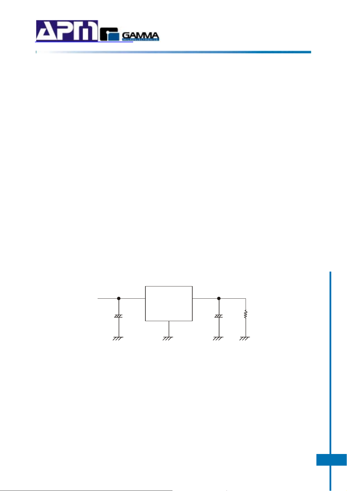
Typical Application Circuits
VIN
C
IN
1µF
(Tantalum)
GM6250-x.x
V
IN
V
SS
Reference Voltage Sources
V
OUT
C
OUT
1µF
(Tantalum)
R
L
GM6250V2.00
www.gammamicro.com.tw
1
V
V
V
查询"GM6250-1.5ST23RG"供应商
300mA ULTRA LOW DROPOUT
POSITIVE VOLTAGE REGULATOR
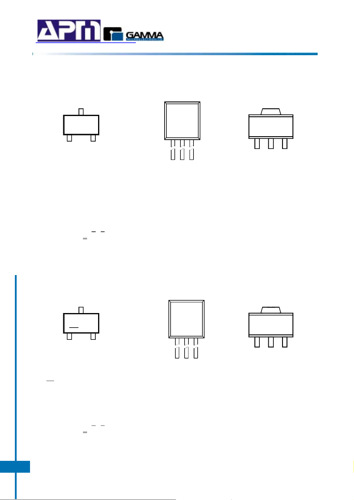
Marking Information and Pin Configurations (Top View)
SOT23 TO92 SOT89
GM6250
EA: Device Code
V: Voltage Code (see next page)
Y: Year (8 = 2008, 9 = 2009 ….)
W: Week Code
IN
2
EAVYW
1
V
SS
3
V
OUT
6250
VV
2
VIN
3
V
OUT
AYWW
1
V
SS
VV: Voltage suffix (18 = 1.8V, 50 = 5.0V…)
A: Assembly Site Code
Y: Year (8 = 2008, 9 = 2009 ….)
WW: Week Code
GM6250
VVAYWW
1
V
SS
2
3
V
IN
V
OUT
Week 1-26 : A – Z
Week 27-52 : A
Week 53 : A
- Z
Marking Information and Pin Configurations – Green Product(Top View)
SOT23 TO92 SOT89
EA: Device Code, Green Product
V: Voltage Code (see next page)
2.00
Y: Year (8 = 2008, 9 = 2009 ….)
W: Week Code
Week 1-26 : A – Z
Week 27-52 : A
Week 53 : A
IN
2
EAVYW
1
VSS
3
V
OUT
- Z
6250G
VV
2
VIN
3
V
OUT
AYWW
1
V
SS
G: Green Product
VV: Voltage suffix (18 = 1.8V, 50 = 5.0V…)
A: Assembly Site Code
Y: Year (8 = 2008, 9 = 2009 ….)
WW: Week Code
GM6250G
VVAYWW
1
V
V
SS
2
3
IN
V
OUT
GM6250
2
GM6250
查询"GM6250-1.5ST23RG"供应商
300mA ULTRA LOW DROPOUT
POSITIVE VOLTAGE REGULATOR
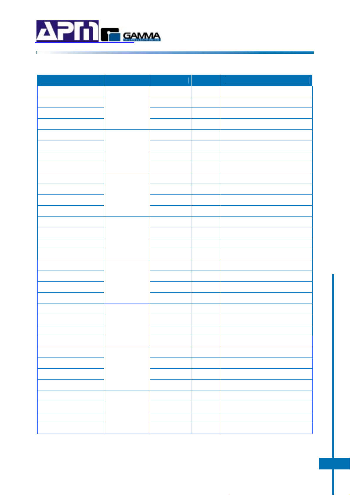
Ordering Information
Ordering Number
GM6250-1.5T92B TO-92 1,000 Units/Bag
GM6250-1.5T92RL TO-92 2,000 Units/Ammo Pack (Tape)
GM6250-1.5ST23R C SOT-23 3,000 Units/Tape and Reel
GM6250-1.5ST89R
GM6250-1.8T92B TO-92 1,000 Units/Bag
GM6250-1.8T92RL TO-92 2,000 Units/Ammo Pack (Tape)
GM6250-1.8ST23R E SOT-23 3,000 Units/Tape and Reel
GM6250-1.8ST89R
GM6250-2.2T92B TO-92 1,000 Units/Bag
GM6250-2.2T92RL TO-92 2,000 Units/Ammo Pack (Tape)
GM6250-2.2ST23R D SOT-23 3,000 Units/Tape and Reel
Output Voltage Voltage Code Package
1.5V
SOT-89 1,000 Units/Tape and Reel
1.8V
SOT-89 1,000 Units/Tape and Reel
2.2V
Shipping
GM6250-2.2ST89R
GM6250-2.5T92B TO-92 1,000 Units/Bag
GM6250-2.5T92RL TO-92 2,000 Units/Ammo Pack (Tape)
2.5V
GM6250-2.5ST23R G SOT-23 3,000 Units/Tape and Reel
GM6250-2.5ST89R
GM6250-2.7T92B TO-92 1,000 Units/Bag
GM6250-2.7T92RL TO-92 2,000 Units/Ammo Pack (Tape)
2.7V
GM6250-2.7ST23R T SOT-23 3,000 Units/Tape and Reel
GM6250-2.7ST89R
GM6250-2.8T92B TO-92 1,000 Units/Bag
GM6250-2.8T92RL TO-92 2,000 Units/Ammo Pack (Tape)
2.8V
GM6250-2.8ST23R H SOT-23 3,000 Units/Tape and Reel
GM6250-2.8ST89R
GM6250-2.85T92B TO-92 1,000 Units/Bag
GM6250-2.85T92RL TO-92 2,000 Units/Ammo Pack (Tape)
2.85V
GM6250-2.85ST23R I SOT-23 3,000 Units/Tape and Reel
SOT-89 1,000 Units/Tape and Reel
SOT-89 1,000 Units/Tape and Reel
SOT-89 1,000 Units/Tape and Reel
SOT-89 1,000 Units/Tape and Reel
GM6250-2.85ST89R
GM6250-3.0T92B TO-92 1,000 Units/Bag
GM6250-3.0T92RL TO-92 2,000 Units/Ammo Pack (Tape)
3.0V
GM6250-3.0ST23R J SOT-23 3,000 Units/Tape and Reel
GM6250-3.0ST89R
SOT-89 1,000 Units/Tape and Reel
SOT-89 1,000 Units/Tape and Reel
GM6250V2.00
3
V
查询"GM6250-1.5ST23RG"供应商
Ordering Information (Continued)
GM6250
300mA ULTRA LOW DROPOUT
POSITIVE VOLTAGE REGULATOR
Ordering Number
GM6250-3.2T92B TO-92 1,000 Units/Bag
GM6250-3.2T92RL TO-92 2,000 Units/Ammo Pack (Tape)
GM6250-3.2ST23R U SOT-23 3,000 Units/Tape and Reel
GM6250-3.2ST89R
GM6250-3.3T92B TO-92 1,000 Units/Bag
GM6250-3.3T92RL TO-92 2,000 Units/Ammo Pack (Tape)
GM6250-3.3ST23R K SOT-23 3,000 Units/Tape and Reel
GM6250-3.3ST89R
GM6250-3.5T92B TO-92 1,000 Units/Bag
GM6250-3.5T92RL TO-92 2,000 Units/Ammo Pack (Tape)
GM6250-3.5ST23R V SOT-23 3,000 Units/Tape and Reel
GM6250-3.5ST89R
GM6250-3.6T92B TO-92 1,000 Units/Bag
GM6250-3.6T92RL TO-92 2,000 Units/Ammo Pack (Tape)
GM6250-3.6ST23R L SOT-23 3,000 Units/Tape and Reel
Output Voltage Voltage Code Package
3.2V
SOT-89 1,000 Units/Tape and Reel
3.3V
SOT-89 1,000 Units/Tape and Reel
3.5V
SOT-89 1,000 Units/Tape and Reel
3.6V
Shipping
GM6250-3.6ST89R
GM6250-4.0T92B TO-92 1,000 Units/Bag
GM6250-4.0T92RL TO-92 2,000 Units/Ammo Pack (Tape)
GM6250-4.0ST23R M SOT-23 3,000 Units/Tape and Reel
GM6250-4.0ST89R
GM6250-4.4T92B TO-92 1,000 Units/Bag
GM6250-4.4T92RL TO-92 2,000 Units/Ammo Pack (Tape)
GM6250-4.4ST23R W SOT-23 3,000 Units/Tape and Reel
GM6250-4.4ST89R
GM6250-4.5T92B TO-92 1,000 Units/Bag
GM6250-4.5T92RL TO-92 2,000 Units/Ammo Pack (Tape)
GM6250-4.5ST23R N SOT-23 3,000 Units/Tape and Reel
GM6250-4.5ST89R
2.00
GM6250-5.0T92B TO-92 1,000 Units/Bag
GM6250-5.0T92RL TO-92 2,000 Units/Ammo Pack (Tape)
GM6250-5.0ST23R Q SOT-23 3,000 Units/Tape and Reel
4.0V
4.4V
4.5V
5.0V
SOT-89 1,000 Units/Tape and Reel
SOT-89 1,000 Units/Tape and Reel
SOT-89 1,000 Units/Tape and Reel
SOT-89 1,000 Units/Tape and Reel
GM6250-5.0ST89R
GM6250
4
SOT-89 1,000 Units/Tape and Reel
GM6250
查询"GM6250-1.5ST23RG"供应商
300mA ULTRA LOW DROPOUT
POSITIVE VOLTAGE REGULATOR
Ordering Information – Green Product
Ordering Number
GM6250-1.5T92BG TO-92 1,000 Units/Bag
GM6250-1.5T92RLG TO-92 2,000 Units/Ammo Pack (Tape)
GM6250-1.5ST23RG C SOT-23 3,000 Units/Tape and Reel
GM6250-1.5ST89RG
GM6250-1.8T92BG TO-92 1,000 Units/Bag
GM6250-1.8T92RLG TO-92 2,000 Units/Ammo Pack (Tape)
GM6250-1.8ST23RG E SOT-23 3,000 Units/Tape and Reel
GM6250-1.8ST89RG
GM6250-2.2T92BG TO-92 1,000 Units/Bag
GM6250-2.2T92RLG TO-92 2,000 Units/Ammo Pack (Tape)
GM6250-2.2ST23RG D SOT-23 3,000 Units/Tape and Reel
Output Voltage Voltage Code Package
1.5V
SOT-89 1,000 Units/Tape and Reel
1.8V
SOT-89 1,000 Units/Tape and Reel
2.2V
Shipping
GM6250-2.2ST89RG
GM6250-2.5T92BG TO-92 1,000 Units/Bag
GM6250-2.5T92RLG TO-92 2,000 Units/Ammo Pack (Tape)
2.5V
GM6250-2.5ST23RG G SOT-23 3,000 Units/Tape and Reel
GM6250-2.5ST89RG
GM6250-2.7T92BG TO-92 1,000 Units/Bag
GM6250-2.7T92RLG TO-92 2,000 Units/Ammo Pack (Tape)
2.7V
GM6250-2.7ST23RG T SOT-23 3,000 Units/Tape and Reel
GM6250-2.7ST89RG
GM6250-2.8T92BG TO-92 1,000 Units/Bag
GM6250-2.8T92RLG TO-92 2,000 Units/Ammo Pack (Tape)
2.8V
GM6250-2.8ST23RG H SOT-23 3,000 Units/Tape and Reel
GM6250-2.8ST89RG
GM6250-2.85T92BG TO-92 1,000 Units/Bag
GM6250-2.85T92RLG TO-92 2,000 Units/Ammo Pack (Tape)
2.85V
GM6250-2.85ST23RG I SOT-23 3,000 Units/Tape and Reel
SOT-89 1,000 Units/Tape and Reel
SOT-89 1,000 Units/Tape and Reel
SOT-89 1,000 Units/Tape and Reel
SOT-89 1,000 Units/Tape and Reel
GM6250-2.85ST89RG
GM6250-3.0T92BG TO-92 1,000 Units/Bag
GM6250-3.0T92RLG TO-92 2,000 Units/Ammo Pack (Tape)
3.0V
GM6250-3.0ST23RG J SOT-23 3,000 Units/Tape and Reel
GM6250-3.0ST89RG
SOT-89 1,000 Units/Tape and Reel
SOT-89 1,000 Units/Tape and Reel
GM6250V2.00
5

V
查询"GM6250-1.5ST23RG"供应商
300mA ULTRA LOW DROPOUT
POSITIVE VOLTAGE REGULATOR
Ordering Information – Green Product (Continued)
GM6250
Ordering Number
GM6250-3.2T92BG TO-92 1,000 Units/Bag
GM6250-3.2T92RLG TO-92 2,000 Units/Ammo Pack (Tape)
GM6250-3.2ST23RG U SOT-23 3,000 Units/Tape and Reel
GM6250-3.2ST89RG
GM6250-3.3T92BG TO-92 1,000 Units/Bag
GM6250-3.3T92RLG TO-92 2,000 Units/Ammo Pack (Tape)
GM6250-3.3ST23RG K SOT-23 3,000 Units/Tape and Reel
GM6250-3.3ST89RG
GM6250-3.5T92BG TO-92 1,000 Units/Bag
GM6250-3.5T92RLG TO-92 2,000 Units/Ammo Pack (Tape)
GM6250-3.5ST23RG V SOT-23 3,000 Units/Tape and Reel
GM6250-3.5ST89RG
GM6250-3.6T92BG TO-92 1,000 Units/Bag
GM6250-3.6T92RLG TO-92 2,000 Units/Ammo Pack (Tape)
GM6250-3.6ST23RG L SOT-23 3,000 Units/Tape and Reel
Output Voltage Voltage Code Package
3.2V
SOT-89 1,000 Units/Tape and Reel
3.3V
SOT-89 1,000 Units/Tape and Reel
3.5V
SOT-89 1,000 Units/Tape and Reel
3.6V
Shipping
GM6250-3.6ST89RG
GM6250-4.0T92BG TO-92 1,000 Units/Bag
GM6250-4.0T92RLG TO-92 2,000 Units/Ammo Pack (Tape)
GM6250-4.0ST23RG M SOT-23 3,000 Units/Tape and Reel
GM6250-4.0ST89RG
GM6250-4.4T92BG TO-92 1,000 Units/Bag
GM6250-4.4T92RLG TO-92 2,000 Units/Ammo Pack (Tape)
GM6250-4.4ST23RG W SOT-23 3,000 Units/Tape and Reel
GM6250-4.4ST89RG
GM6250-4.5T92BG TO-92 1,000 Units/Bag
GM6250-4.5T92RLG TO-92 2,000 Units/Ammo Pack (Tape)
GM6250-4.5ST23RG N SOT-23 3,000 Units/Tape and Reel
GM6250-4.5ST89RG
2.00
GM6250-5.0T92BG TO-92 1,000 Units/Bag
GM6250-5.0T92RLG TO-92 2,000 Units/Ammo Pack (Tape)
GM6250-5.0ST23RG Q SOT-23 3,000 Units/Tape and Reel
4.0V
4.4V
4.5V
5.0V
SOT-89 1,000 Units/Tape and Reel
SOT-89 1,000 Units/Tape and Reel
SOT-89 1,000 Units/Tape and Reel
SOT-89 1,000 Units/Tape and Reel
GM6250-5.0ST89RG
GM6250
6
SOT-89 1,000 Units/Tape and Reel

GM6250
查询"GM6250-1.5ST23RG"供应商
300mA ULTRA LOW DROPOUT
POSITIVE VOLTAGE REGULATOR
Absolute Maximum Ratings
PARAMETER SYMBOL RATINGS UNITS
Input Voltage VIN 12 V
Output Current I
Output Voltage V
SOT-23 150
Continuous Total Power
Dissipation
SOT-89 500
TO-92
Operating Ambient Temperature T
Storage Temperature T
Lead Temperature (Soldering, 10 sec) + 260 ℃
500 mA
OUT
V
OUT
P
D
– 0.3 to VIN +0.3 V
SS
mW
300
- 40 to 125 ℃
A
- 65 to 150 ℃
stg
Block Diagram
VIN
V
SS
V
OUT
Current
Limit
Voltage
Reference
GM6250V2.00
7

V
查询"GM6250-1.5ST23RG"供应商
GM6250
300mA ULTRA LOW DROPOUT
POSITIVE VOLTAGE REGULATOR
Electrical Characteristics (T
= 25℃, V
A
IN
= V
+ 1V unless otherwise noted)
OUT
Parameter Symbol Condition Min Typ Max Unit
GM6250-1.5 1.470 1.500 1.530
GM6250-2.2 1.764 2.200 2.236
GM6250-2.5 2.450 2.500 2.550
GM6250-2.7 2.646 2.700 2.754
GM6250-2.8 2,744 2.800 2.856
GM6250-3.0 2.940 3.000 3.060
Output Voltage
Line Regulation
Load Regulation
Dropout
Voltage
Current Consumption IQ 1.0 2.9 µA
GM6250-3.2 3.136 3.200 3.264
V
GM6250-3.3 3.234 3.300 3.366
GM6250-3.5 3.430 3.500 3.570
GM6250-3.6 3.528 3.600 3.672
GM6250-4.0 3.920 4.000 4.080
GM6250-4.4 4.312 4.400 4.488
GM6250-4.5 4.410 4.500 4.590
GM6250-5.0
V
> 2.7V 0.4 0.7
OUT
2.0V < V
V
OUT
OUT
< 2.0V
< 2.7V
OUT
∆V
OI
∆V
1mA < I
OL
∆V
= 40mA, VIN = V
I
OUT
I
OUT
+ 1V < VIN < 10V
V
OUT
I
OUT
= 40mA,
< 80mA
OUT
= 160mA
OUT
+ 1V
V
4.900 5.000 5.100
0.2 0.3 %/V
0.02 0.03 %/mA
0.55 0.85
0.9 1.3
V
Output Current Limit ICL 500 mA
Power Supply Rejection Ration PSRR 10kHz 10 dB
2.00
GM6250
8

GM6250
查询"GM6250-1.5ST23RG"供应商
Application Note
Notes on Usage
1. It is recommended to operate the GM6250 series within the stipulated absolute maximum ratings
as the IC is liable to malfunction it is operated outside the ratings.
2. There is a possibility of heat or oscillation as a result of the impedance present between the
power supply and the IC's input. Where impedance is greater 10Ω, it is recommend to use a
capacitor (C
3. With a large output current, operations can be stabilized by increasing capacitor size (C
is too small and capacitance of (CL) is increased, there is a possibility of oscillation due to input
impedance. In such case, operation can be stabilized by either increasing the size of C
decreasing the size of C
4. Please ensure the output current (I
stipulated continuous for total power dissipation value (Pd) for the package.
CALCULATING POWER DISSIPATION
The GM6250 series precision linear regulators include thermal shutdown and current limit circuitry to
protect the devices. However, high power regulators normally operate at high junction temperatures so
it is important to calculate the power dissipation and junction temperatures accurately to be sure that
you use and adequate heat sink.
) of at least 1µF at the input terminal.
IN
.
L
) is less than Pd ÷ (V
OUT
300mA ULTRA LOW DROPOUT
POSITIVE VOLTAGE REGULATOR
). If C
IN
or
IN
- V
IN
) and does not exceed the
OUT
IN
The thermal characteristics of an IC depend four factors:
1. Maximum Ambient Temperature T
2. Power Dissipation P
3. Maximum Junction Temperature T
4. Thermal Resistance Junction to ambient R
These relationship of these four factors is expressed by equation :
Maximum ambient temperature and power dissipation are determined by the design while the
maximum junction temperature and thermal resistance depend on the manufacturer and the package
type.
(Watts)
D
A
J
(℃)
(℃)
(℃/W)
JA
TJ =
TA + P
D
X R
JA
GM6250V2.00
9

V
A
A
A
y
A
p
查询"GM6250-1.5ST23RG"供应商
300mA ULTRA LOW DROPOUT
POSITIVE VOLTAGE REGULATOR
Typical Performance Characteristics (for GM6250-3.0)
GM6250
(V)
OUT
V
Voltage:
Output
3.1
3.0
(V)
OUT
2.9
2.8
Output Voltage – V
2.7
3.20
3.00
2.80
2.60
2.40
2.20
T
= 25°C
OPR
2.5
0
20
8060 40
Output Current: I
Figure 1: Output Voltage vs.
Output Current
I
=1mA
10m
40mA
3.0
OUT
Input Voltage: VIN (V)
Figure 3: Output Voltage vs.
Input voltage
100
120
OUT
V
IN
C
IN
CL = 11
140
(mA)
T
= 25
OPR
CIN=1µF
CL=1µF
= 4V
= 1
160
µF
1.0
(V)
DIF
0.8
0.6
0.4
0.2
0.0
CIN = 1
CL = 11
µF
µF
T
OPR
= 25°C
µF
Input-Output Voltage Difference– V
180
°C
3.5
-0.2
80604020
100
140
120
Figure 2: Input/ Output Voltage differential
vs. Out
)
V
(
OUT
V
:
age
t
ol
V
t
pu
t
u
O
ut Current
3.10
3.05
3.00
2.95
2.90
40m
I
OUT
T
OPR
CIN=1µF
CL=1µF
2.85
3 10
4 5 6 8
Input Voltage: VIN(V)
Figure 4: Output Voltage vs.
Input voltage
7
160
=1mA
10m
= 25°C
9
180
3.0
(µA)
SS
2.0
Current:I
1.0
Supply
2.00
0
0
T
= 25°C
OPR
2
4
Input Voltage: VIN(V)
6
8
Figure 5: Supply Current vs.
Input Voltage
10
2.50
)
2.25
(µ
SS
t: I
2.00
Curren
uppl
1.75
S
1.50
T
= 25°C
OPR
4 5 6 7 8 9
3
Input Voltage: VIN(V)
Figure 6: Supply Current vs.
Input Voltage
10
GM6250
10

GM6250
查询"GM6250-1.5ST23RG"供应商
300mA ULTRA LOW DROPOUT
POSITIVE VOLTAGE REGULATOR
Typical Performance Characteristics (for GM6250-3.0, continued)
6
4
(V)
2
IN
0
-2
-4
Input Voltage – V
-6
Input Voltage
Output Voltage
Time (0.4msec/
I
= 1mA
OUT
CL = 1µF
div)
6
5
4
3
2
1
0
Figure 7: Input Transient Response 1
(dB)
:RR
Rate
60
50
40
30
VIN = 4VDC + 1V
I
= 40mA
OUT
CL = 1µF
PPAC
(V)
IOUT
Output Voltage – V
6
5
(V)
IN
4
3
2
Input Voltage – V
1
Input Voltage
I
= 1mA
OUT
CL = 1µF
Output Voltage
Time (1msec/
div)
Figure 8: Input Transient Response 2
5.0
4.5
4.0
3.5
3.0
2.5
(V)
IOUT
Output Voltage – V
20
Rejection
10
Ripple
0
0.01
0.1 1
Ripple Frequency: f (kHz)
Figure 9: Ripple Rejection Rate
10
GM6250V2.00
11

V
查询"GM6250-1.5ST23RG"供应商
Package Outline Dimensions – SOT 23
GM6250
300mA ULTRA LOW DROPOUT
POSITIVE VOLTAGE REGULATOR
0.110 - 0.120
(2.80 - 3.04)
0.047 - 0.055
(1.20 - 1.40)
0.075
Typ.
(1.91)
0.0150 - 0.0200
(0.382 - 0.508)
0.083 - 0.104
(2.11 - 2.62)
0.037
(0.93)
Package Outline Dimensions – SOT 89
0.003 - 0.007
(0.08 - 0.18)
Typ.
0.0005 - 0.0040
(0.025 - 0.102)
0.013 - 0.017
(0.34 - 0.44)
0 - 8 typ
0.173 - 0.181
(4.39 - 4.59)
0.061 REF
(1.550 REF)
0.084 - 0.090
(2.13 - 2.28)
0.155 - 0.167
(3.94 - 4.24)
0.035 - 0.047
(0.89 - 1.19)
0.013 - 0.021
(0.320 - 0.520)
0.059 BSC
(1.49) BSC
0.118 BSC
(2.99) BSC
2.00
0.090 - 0.102
(2.28 - 2.59)
0.016 - 0.023
(0.400 - 0.580)
8
0.055 - 0.063
(1.39 - 1.60)
0.014 - 0.017
(0.35 - 0.43)
GM6250
12

GM6250
查询"GM6250-1.5ST23RG"供应商
Package Outline Dimensions – TO 92
3.85 - 4.19
2.10 - 2.27
0.4 - 0.55
Typ.
4.7 - 5.2
300mA ULTRA LOW DROPOUT
POSITIVE VOLTAGE REGULATOR
4.9 - 5.2
12.7 - 14.2
1.22 - 1.32
Dimensions are in millimeters
GM6250V2.00
1

V
查询"GM6250-1.5ST23RG"供应商
Ordering Number
G
M 6250 - 2.2
T92
GM6250
300mA ULTRA LOW DROPOUT
POSITIVE VOLTAGE REGULATOR
B
G
APM
Gamma
Micro
Circuit
Type
Output
Voltage
2.2 = 2.2V
2.5 = 2.5V
3.3 = 3.3V
5.0 = 5.0V
Package Type Shipping Type
T92: TO 92
ST89: SOT 89
ST23: SOT 23
B: Bag
RL: Ammo Pack
(Tape)
T: Tube
R: T
ape & Reel
Blank:Pb-free
G:Green
Note:
Pb-free products:
♦ RoHS compliant and compatible with the current require-ments of IPC/JEDEC J-STD-020.
♦ Suitable for use in SnPb or Pb-free soldering processes with 100% matte tin (Sn) plating.
Green products:
♦ Lead-free (RoHS compliant)
♦ Halogen free(Br or Cl does not exceed 900ppm by weight in homogeneous material and total of
Br and Cl does not exceed 1500ppm by weight)
2.00
GM6250
14

查询"GM6250-1.5ST23RG"供应商
This datasheet has been downloaded from:
www.EEworld.com.cn
Free Download
Daily Updated Database
100% Free Datasheet Search Site
100% Free IC Replacement Search Site
Convenient Electronic Dictionary
Fast Search System
www.EEworld.com.cn
All Datasheets Cannot Be Modified Without Permission
Copyright © Each Manufacturing Company
 Loading...