

Page 1

Chapter 2
Hardware Installation
This chapter gives you a step-by-step procedure on how to install your system.
Follow each section accordingly.
Caution: Electrostatic discharge (ESD) can
damage your processor, disk drives, expansion
boards, and other components. Always
observe the following precautions before you
install a system component.
1. Do not remove a component from its
protective packaging until you are ready
to install it.
2. Wear a wrist ground strap and attach it to
a metal part of the system unit before
handling a component. If a wrist strap is
not available, maintain contact with the
system unit throughout any procedure
requiring ESD protection.
2-1
Page 2
Hardware Installation
1
2
3
LED
IrDA
JP14
FAN
CPU FAN
PWR2
WKUP
COM1
PRINTER
COM2
JP23
SCSI
Wide-SCSI
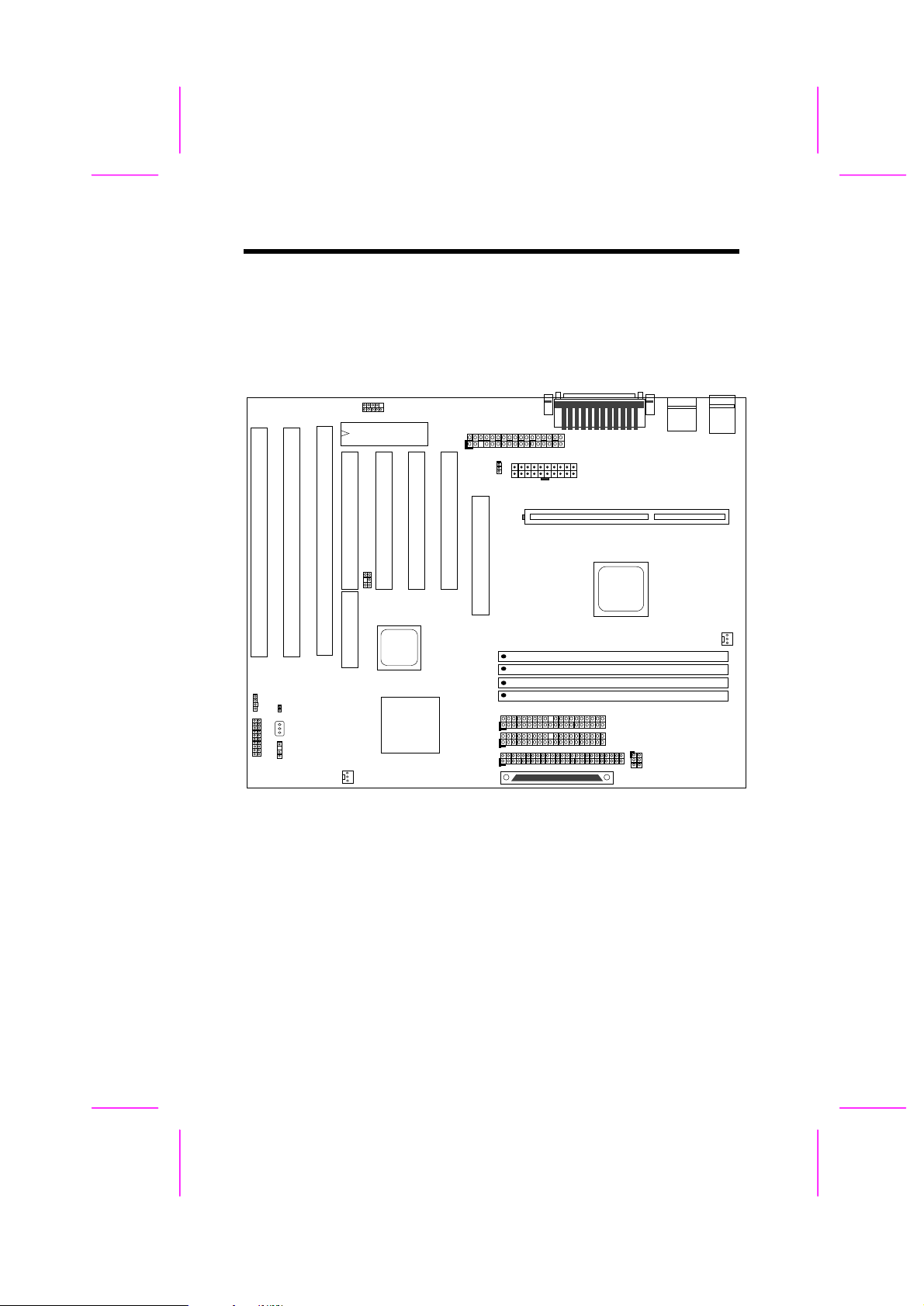
2.1 Jumper and Connector Locations
The following figure shows the locations of the jumpers and connectors on the
system board:
I
S
A
HDD
PANEL
I
S
A
SPWR
LAN Wakeup
BIOS
I
S
A
P
P
C
C
I
I
3
4
SB-Link
R
A
I
D
P
O
R
T
P
P
C
C
I
I
1
2
FDC
A
G
P
CPU SLOT 1
IDE2
IDE1
USB
DIMM4
DIMM3
DIMM2
DIMM1
PS/2
KB
2-2
Page 3

Hardware Installation
Jumpers:
JP14: Clear CMOS
JP23: AGP Ratio
Connectors:
PS2: PS/2 mouse connector
KB: PS/2 keyboard connector
COM1: COM1 connector
COM2: COM2 connector
PRINTER: Printer connector
PWR2: ATX power connector
USB: USB connector
FDC: Floppy drive connector
IDE1: IDE1 primary channel
IDE2: IDE2 secondary channel
CPUFAN: CPU Fan connector
FAN: Housing Fan Connector
IrDA: IrDA (Infrared) connector
HDD LED: HDD LED connector
PANEL: Front panel (Multifunction) connector
SPWR: ATX Soft-Power Switch Connector
MODEM-WKUP: Modem Wake Up Connector
LAN-WKUP: LAN Wake Up Connector
SB-LINK: Creative PCI sound card connector
2-3
Page 4
Hardware Installation
2.2 Jumpers
With the help of Pentium II VID signal and SMbus, this motherboard is jumperless design.
2.2.1 Selecting the CPU Frequency
Pentium II VID signal and SMbus clock generator provide CPU voltage autodetection and allow user to set CPU frequency through CMOS setup, no jumper
or switch is needed. The correct CPU information is saved into EEPROM, with
these technologies, the disadvantages of Pentium base jumper-less design are
eliminated. There will be no worry of wrong CPU voltage detection and no need
to re-open the housing if CMOS battery loss.
The CPU frequency selection is set by going into:
BOIS Setup à Chipset Features Setup à CPU Clock Frequency
(The possible setting is 66, 68.5, 75, 83.3, 100, 103, 112 and 133.3 MHz)
BOIS Setup à Chipset Features Setup à CPU Clock Ratio
(The possible setting is 1.5x, 2x, 2.5x, 3x, 3.5x, 4x, 4.5x, 5x, 5.5x, 6x, 6.5x, 7x,
7.5x, and 8x)
Core frequency = Ratio * External bus clock
INTEL Pentium II CPU Core Frequency Ratio External Bus Clock
Pentium II - 233 233MHz = 3.5x 66MHz
Pentium II - 266 266MHz = 4x 66MHz
Pentium II - 300 300MHz = 4.5x 66MHz
Pentium II - 333 333MHz = 5x 66MHz
Pentium II - 350 350MHz= 3.5x 100MHz
Pentium II - 400 400MHz= 4x 100MHz
Pentium II - 450 450MHz= 4.5x 100MHz
Celeron 266 266MHz= 4x 66MHz
Celeron 300 300MHz 4.5x 66MHz
Celeron 300A 300MHz 4.5x 66MHz
Celeron 333 333MHz 5x 66MHz
2-4
Page 5
Hardware Installation
3
3
Warning: INTEL 440BX chipset supports maximum 100MHz
external CPU bus clock, the 103, 112 and 133.3MHz are for
internal test only. These settings exceed the specification
of BX chipset, which may cause serious system damage.
2.2.2 Setting the CPU Voltage
This motherboard supports Pentium II VID function, the CPU core voltage is
automatically detected, the range is from 1.3V to 3.5V.
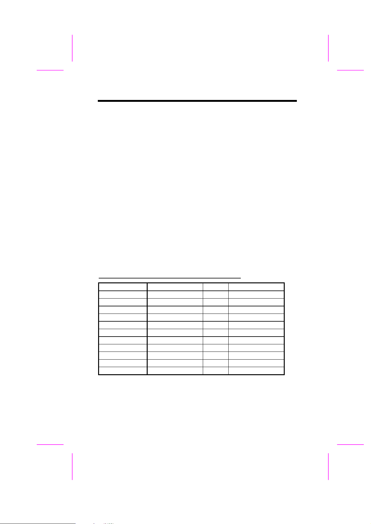
2.2.3 Clearing the CMOS
JP14
1-2
2-3
Clear CMOS
Normal operation
(default)
Clear CMOS
You need to clear the CMOS if you forget your
system password. To clear the CMOS, follow
the procedures listed below:
JP14
1
2
Normal Operation
JP14
1
2
Clear CMOS
(default)
The procedure to clear CMOS:
1. Turn off the system and unplug the AC power.
2. Remove ATX power cable from connector PWR2.
3. Locate JP14 and short pins 2-3 for a few seconds.
4. Return JP14 to its normal setting by shorting pins 1-2.
5. Connect ATX power cable back to connector PWR2.
6. Turn on the system power.
7. Press during bootup to enter the BIOS Setup Utility and specify a
new password, if needed.
Tip: If your system hangs or fails to boot because of
over-clocking, please clear CMOS and the system will go
back to default setting (233MHz).
2-5
Page 6

Hardware Installation
Tip: Except using JP14, you may also press <Home>
key. By this smart design, it would be more convenient to
clear CMOS. For using this function, you just need to
press <Home> key first and then press Power button at
the same time. After doing this, the system will return to
the default setting (233MHz).
2-6
Page 7
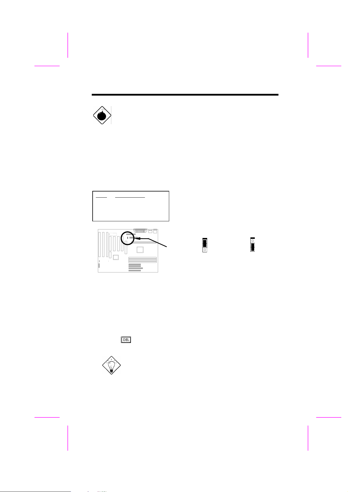
2.2.4 AGP Ratio
5
6
5
6
5
6
Hardware Installation
JP23
1-2
3-4
5-6
AGP Ratio
Auto (default)
2/3
1/1
To improve system performance, AX6B has
implemented this jumper for AGP to synchronize the
CPU 100Mhz (or above) external frequency. We
recommend you choose a better AGP card for
overclocking. Some AGP cards can not take 100MHz
bus frequency and may cause overclocking failure.
JP23
1
3
JP23
2
4
1
3
JP23
2
4
1
2
3
4
Auto
2/3
1/1
(Default)
There is a "66/100" signal pin from CPU for BX chipset to automatically identify
AGP clock, this is important for jumperless design. When a 66MHz Pentium II
CPU is used, the north bridge will synchronize the CPU external frequency and
the AGP bus frequency. Therefore, when you set the CPU external frequency to
100MHz, the AGP bus will also runs at 100MHz.
With 100MHz Pentium II CPU, the north bridge automatically set AGP frequency
to 2/3 AGP frequency. In other words, the AGP card will still runs at 66MHz while
the CPU is running at 100MHz external frequency.
Except Auto setting, you may also set this jumper to 2/3 or 1/1. Below is a table
for better understanding:
CPU Type 66/100 signal Bus clock AGP clock JP23
66MHz Low 66MHz 66MHz 1-2
66MHz Low 100MHz 100MHz 1-2
66MHz Low 100MHz 66MHz 3-4
100MHz High 100MHz 66MHz 1-2
100MHz High 100MHz 66MHz 3-4
100MHz High 100MHz 100MHz 5-6
100MHz High 133MHz 88.6MHz 1-2
100MHz High 133MHz 88.6MHz 3-4
100MHz High 133MHz 133MHz 5-6
Warning: The specification of AGP is maximum 66Mhz
clock. If the bus clock is larger than 66MHz, setting this
item to Enabled may cause serious system damage.
2-7
Page 8

Hardware Installation
5V SB
2.3 Connectors
2.3.1 Power Cable
The ATX power supply uses 20-pin connector shown below. Make sure you
plug in the right direction.
Caution: Make sure that the power supply is
off before connecting or disconnecting the
power cable.
+5V
3.3V
3.3V
PWR2
+5V
2.3.2 ATX Soft-Power Switch Connector
The ATX soft-power switch connector is a 2-pin header on the system board.
Locate the power switch cable from your ATX housing. It is 2-pin female
connector from the housing front panel. Plug this connector to the soft-power
switch connector marked SPWR.
1
2
SPWR
2-8
Page 9

Hardware Installation
SENSE
PS/2 Mouse
2.3.3 Fan
Plug in the fan cable to the 3-pin fan connector onboard. The fan connector is
marked CPU FAN and FAN on the system board.
+12V
GND
CPUFAN and FAN
Note: Attach fan cable to either CPU FAN connector or
FAN connector. Both of these two fans connectors can
support hardware monitoring function, however, you can
only use the CPU FAN connector to control the fan
power ON/OFF.
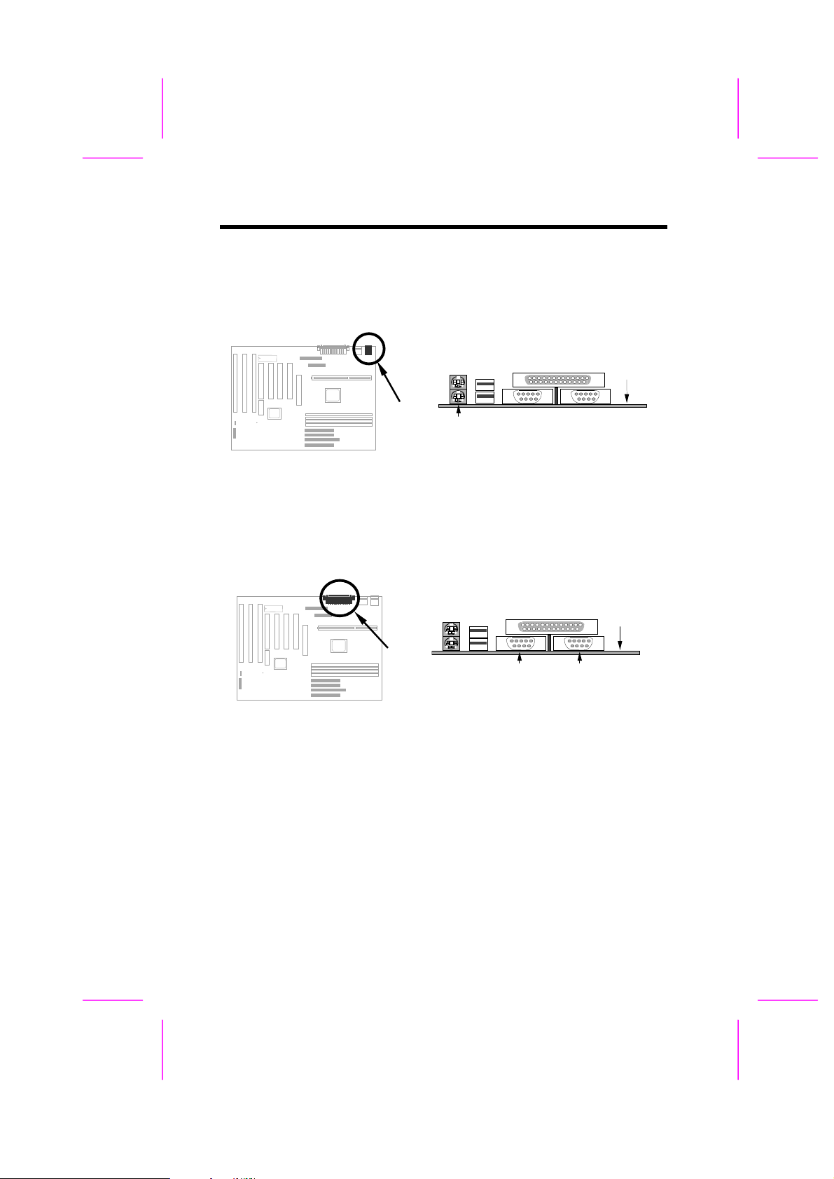
2.3.4 PS/2 Mouse
The onboard PS/2 mouse connector is a 6-pin Mini-Din connector marked PS2.
The view angle of drawing shown here is from back panel of the housing.
2-9
PCB
Page 10
Hardware Installation
PS/2 KB
COM1
COM2
2.3.5 Keyboard
The onboard PS/2 keyboard connector is a 6-pin Mini-Din connector marked
KB2. The view angle of drawing shown here is from back panel of the
housing.
PCB
2.3.6 Serial Devices (COM1/COM2)
The onboard serial connectors are 9-pin D-type connector on the back panel of
mainboard. The serial port 1 connector is marked as COM1 and the serial port
2 connector is marked as COM2.
2-10
PCB
Page 11

Hardware Installation
PRINTER
USB
2.3.7 Printer
The onboard printer connector is a 25-pin D-type connector marked PRINTER.
The view angle of drawing shown here is from back panel of the housing.
PCB
2.3.8 USB Device
You can attach USB devices to the USB connector. The motherboard
contains two USB connectors, which are marked as USB.
PCB
2-11
Page 12

Hardware Installation
34
33
1
40
2
39
1
40
2
39
2.3.9 Floppy Drive
Connect the 34-pin floppy drive cable to the floppy drive connector marked as
FDC on the system board.
2
1
FDC
2.3.10 IDE Hard Disk and CD ROM
This mainboard supports two 40 pin IDE connectors marked as IDE1 and
IDE2. IDE1 is also known as primary channel and IDE2 as secondary
channel, each channel supports two IDE devices that makes total of four
devices.
In order to work together, the two devices on each channel must be set
differently to master and slave mode, either one can be hard disk or CDROM.
The setting as master or slave mode depends on the jumper on your IDE
device, please refer to your hard disk and CDROM manual accordingly.
Connect your first IDE hard disk to master mode of the primary channel. If you
have second IDE device to install in your system, connect it as slave mode on
the same channel, and the third and fourth device can be connected on
secondary channel as master and slave mode respectively.
2-12
IDE2
IDE1
Page 13

Hardware Installation
(3rd)
(4th)
1
50
2
49
1
68
2
67
Caution: The specification of IDE cable is
maximum 46cm (18 inches), make sure your
cable does not excess this length.
Caution: For better signal quality, it is
recommended to set far end side device to
master mode and follow the suggested
sequence to install your new device. Please
refer to following figure.
IDE2 (Secondary Channel)
Slave
IDE1 (Primary Channel)
Slave
(2nd)
Master
Master
(1st)
2.3.11 SCSI Devices
Connect your SCSI devices to the on board 68-pin WIDE-SCSI or 50-pin
SCSI connector.
SCSI
WIDE-SCSI
2-13
Page 14

Hardware Installation
4
+
+
4
+
+
4
+
+
2.3.12 Hard Disk LED
The HDD LED connector is marked as HDD
LED on the board. This connector is designed
for different type of housing, actually only two
pins are necessary for the LED. If your housing
has four pin connector, simply plug it in. If you
have only two pin connector, please connect to
pin 1-2 or pin 3-4 according to the polarity.
1
2
3
HDD LED
4-pin connector
2.3.13 SB-LINK
SB-LINK is used to connect Creative PCI sound
card. If you have a Creative PCI sound card
installed, it is necessary to link the card to this
connector for compatibility issue under DOS
environment.
Pin
1
2
3
4
Description
HDD LED
GND
GND
HDD LED
1
2
3
HDD LED
2-pin
connector at
pin 1-2
Pin
1
2
3
4
5
6
1
2
3
HDD LED
2-pin
connector at
pin 3-4
Description
GNT#
GND
NC
REQ#
GND
SIRQ#
2-14
1 2
5 6
SB-LINK
Page 15

2.3.14 Panel Connector
1
11
10
20
+
+
+
+
1
111020
Hardware Installation
The Panel (multifunction) connector is
a 20-pin connector marked as PANEL
on the board. Attach the power LED,
keylock, speaker, and reset switch to
the corresponding pins as shown in
the figure.
Some housings have a five-pin
connector for the keylock and power
LED Since power LED and keylock
are aligned together, you can still use
this kind of connector.
ACPI & POWER LED
Keylock
ACPI &
Power LED
Speaker
1
11
GND
KEYLOCK
GND
+5V
SPEAKER
+5V
GND
NC
SPEAKER
10 20
PANEL
Reset
PANEL
+5V
GND
Reserved
GND
NC
NC
GND
NC
RESET
GND
Other housings may have a 12-pin
connector. If your housing has this
type of connector, connect it to
PANEL as shown in the figure. Make
sure that the red wire of the
connector is connected to +5V.
+5V
PANEL
2-15
Page 16

Hardware Installation
1 3 5 7 9
2 4 6 8 10
2.3.15 IrDA Connector
The IrDA connector can be configured to support wireless infrared module,
with this module and application software such as Laplink or Win95 Direct
Cable Connection, user can transfer files to or from laptops, notebooks, PDA
and printers. This connector supports HPSIR (115.2Kbps, 2 meters), ASK-IR
(56Kbps) and Fast IR (4Mbps, 2 meters).
Install infrared module onto IrDA
connector and enable infrared function
from BIOS setup, make sure to have
correct orientation when you plug onto
IrDA connector.
Pin
1
3
4
5
6
7
9
IrDA
Description
+5V
FIRRX (FAST IR)
CIRRX
IRRX (STANDARD IR)
5VSB
GND
IRTX (STANDARD IR)
2-16
Page 17

Hardware Installation
3
2.3.16 Modem Wake-up Connector
This mainboard implements special circuit to support
Modem Ring-On, both Internal Modem Card (AOpen
MP56) and external box Modem are supported. Since
Internal Modem card consumes no power when system
power is off, it is recommended to use Internal Modem.
To use AOpen MP56, connect 4-pin cable from RING
connector of MP56 to MODEM-WKUP connector on
the mainboard.
1
2
3
4
MODEM-WKUP
2.3.17 LAN Wake-up Connector
This mainboard implements a LAN-WKUP connector.
To use LAN Wake-up function, you need a network
card that supports this feature. In addition, you also
need to install a network management software, such
as ADM.
Pin
1
2
3
4
Pin
1
2
3
Description
+5V SB
NC
RING
GND
Description
+5V SB
GND
LID
1
2
LAN-WKUP
2-17
Page 18

Hardware Installation
168
2.4 Configuring the System Memory
The DIMM types supported are SDRAM
(Synchronous DRAM) and Registered
SDRAM. This mainboard has four 168 pin
DIMM sockets (Dual-in-line Memory Module)
that allow you to install system memory up to
1GB. But note that mixing SDRAM and
Registered SDRAM is not allowed, you can
install one of the DRAM types only.
PIN 1
Warning: This motherboard does not support EDO
DRAM.
DIMM modules can be identified by the following factors:
I. Size: single side, 1Mx64 (8MB), 2Mx64 (16MB), 4Mx64 (32MB), 8Mx64
(64MB), 16Mx64 (128MB), and double side, 1Mx64x2 (16MB), 2Mx64x2
(32MB), 4Mx64x2 (64MB), 8Mx64x2 (128MB).
2-18
Tip: Here is a trick to check if your DIMM is
single-side or double-side -- if there are traces
connected to golden finger pin 114 and pin 129 of
the DIMM, the DIMM is probably double-side;
otherwise, it is single-side. Following figure is for
your reference.
Pin 129
Pin 114
Note: 1GB memory is achieved by using 64M bit
Registered SDRAMs.
Page 19

Hardware Installation
II. Speed: Normally marked as -12, which means the clock cycle time is 12ns
and maximum clock of this SDRAM is 83MHz. Sometimes you can also find
the SDRAM marked as -67, which means maximum clock is 67MHz.
Caution: Some SDRAMs marked as -10 may
work fine with 100 MHz CPU clock, but not all
this kind of modules can work properly under
100MHz external clock. We suggest you
choose and install SDRAMs that match PC 100
specification if 100MHz or above CPU clock is
selected.
III. Buffered and non-buffered: This motherboard supports non-buffered
DIMMs. You can identify non-buffered DIMMs and buffered DIMMs
according to the position of the notch, following figure is for your reference:
Reserved
non-buffered
buffered
Because the positions are different, only non-buffered DIMMs can be inserted
into the DIMM sockets on this motherboard. Although most of DIMMs on
current market are non-buffered, we still recommend you to ask your dealer
for the correct type.
IV. 2-clock and 4-clock signals: Although both of 2-clock and 4-clock signals
are supported by AX6B, we strongly recommend you to choose 4-clock
SDRAM in consideration of reliability.
Tip: To identify 2-clock and 4-clock SDRAM, you
may check if there are traces connected to golden
finger pin 79 and pin 163 of the SDRAM. If there
are traces, the SDRAM is probably 4-clock;
Otherwise, it is 2-clock.
V. Parity: This motherboard supports standard 64 bit wide (without parity) and
72-bit wide (with parity) DIMM modules.
VI. SPD support: BIOS will automatically detect DIMM with SPD, and set to
appropriate timing. DIMMs without SPD are still able to work fine on this
board, but BIOS POST screen will give you a warning message that you
use a DIMM without SPD.
2-19
Page 20

Hardware Installation
There is no jumper setting required for the memory size or type. It is
automatically detected by the system BIOS, and the total memory size is to add
them together.
Total Memory Size = Size of DIMM1 + Size of DIMM2 + Size of DIMM3 +
Size of DIMM4
Following table list the recommended SDRAM combinations of DIMM:
DIMM
Data chip
1M by 16 1Mx64 x1 4 8MB Yes
1M by 16 1Mx64 x2 8 16MB Yes
2M by 8 2Mx64 x1 8 16MB Yes
2M by 8 2Mx64 x2 16 32MB Yes
4M by 16 4Mx64 x1 4 32MB Yes
4M by 16 4Mx64 x2 8 64MB Yes
8M by 8 8Mx64 x1 8 64MB Yes
8M by 8 8Mx64 x2 16 128MB Yes
DIMM
Data chip
2M by 32 2Mx64 x1 2 16MB Yes, but not tested.
2M by 32 2Mx64 x2 4 32MB Yes, but not tested.
Bit size
per side
Bit size
per side
Single/
Double side
Single/
Double side
Chip
count
Chip
count
DIMM size Recommended
DIMM size Recommended
Following table are possible SDRAM combinations that is NOT recommended:
DIMM
Data chip
4M by 4 4Mx64 x1 16 32MB No
4M by 4 4Mx64 x2 32 64MB No
16M by 4 16Mx64 x1 16 128MB No
Bit size
per side
Single/
Double side
Chip
count
DIMM size Recommended
2-20
Page 21

Hardware Installation
For getting the best performance and stability under 100MHz or above external
clock, we strongly recommend you use PC 100 SDRAM. The PC 100 SDRAM
that AOpen had tested are listed below.
Size Vendor Model Single/Double Chip Count
16M Micron MT48LC2M8A1-08 x1 8
16M TI TMX626812BDGE-10A x1 8
16M Hyundai HY57V168010CTC-10 x1 8
32M Fujitsu 81F16822D-A10-7JF X2 16
32M Micron MT48LC2M8A1-08 x2 16
32M Hyndai HY57V168010CTC-10 x1 16
32M NEC D4516821AG5-A10-7JF x1 16
32M SEC KM48S2020CT-GH x1 16
32M LGS GM72V661641CT7J x1 4
64M Fujitsu 81F64842B-103FN x2 16
64M Mitsubishi M5M4V64S30ATP-10 x1 8
64M NEC D4564841G5-A10-9JF x1 8
64M SEC KM48S8030BT-GH x1 8
64M Toshiba TC59S6408FTL-80H x1 8
64M LGS GM72V661641CT7J x2 8
64M LGS GM72V66841CT7J x1 9
128M LGS GM72V66841CT7J x2 18
128M Simens HYS72V16220GU x2 18
Memory error checking is supported by parity check. To use parity check you
need 72 bit DIMM (64+8 bit parity), which are automatically detected by BIOS.
2-21
Page 22

Hardware Installation
Warning: The driving capability of new generation chipset is
limited because the lack of memory buffer (to improve
performance). This makes DRAM chip count an important
factor to be taking into consideration when you install DIMM.
Unfortunately, there is no way that BIOS can identified the
correct chip count, you need to calculate the chip count by
yourself. The simple rule is: By visual inspection, use only
DIMM which is less than 16 chips.
Tip: The parity mode uses 1 parity bit for each byte, normally it
is even parity mode, that is, each time the memory data is
updated, parity bit will be adjusted to have even count "1" for
each byte. When next time, if memory is read with odd
number of "1", the parity error is occurred and this is called
single bit error detection.
2-22
 Loading...