

Page 1

Chapter 2
Hardware Installation
This chapter gives you a step-by-step procedure on how to install your
system. Follow each section accordingly.
2.1 ESD Precautions
Electrostatic discharge (ESD) can damage your processor, disk drives,
expansion boards, and other components. Always observe the following
precautions before you install a system component.
1. Do not remove a component from its protective packaging until you are
ready to install it.
2. Wear a wrist ground strap and attach it to a metal part of the system unit
before handling a component. If a wrist strap is not available, maintain
contact with the system unit throughout any procedure requiring ESD
protection.
2-1
Page 2
Hardware Installation
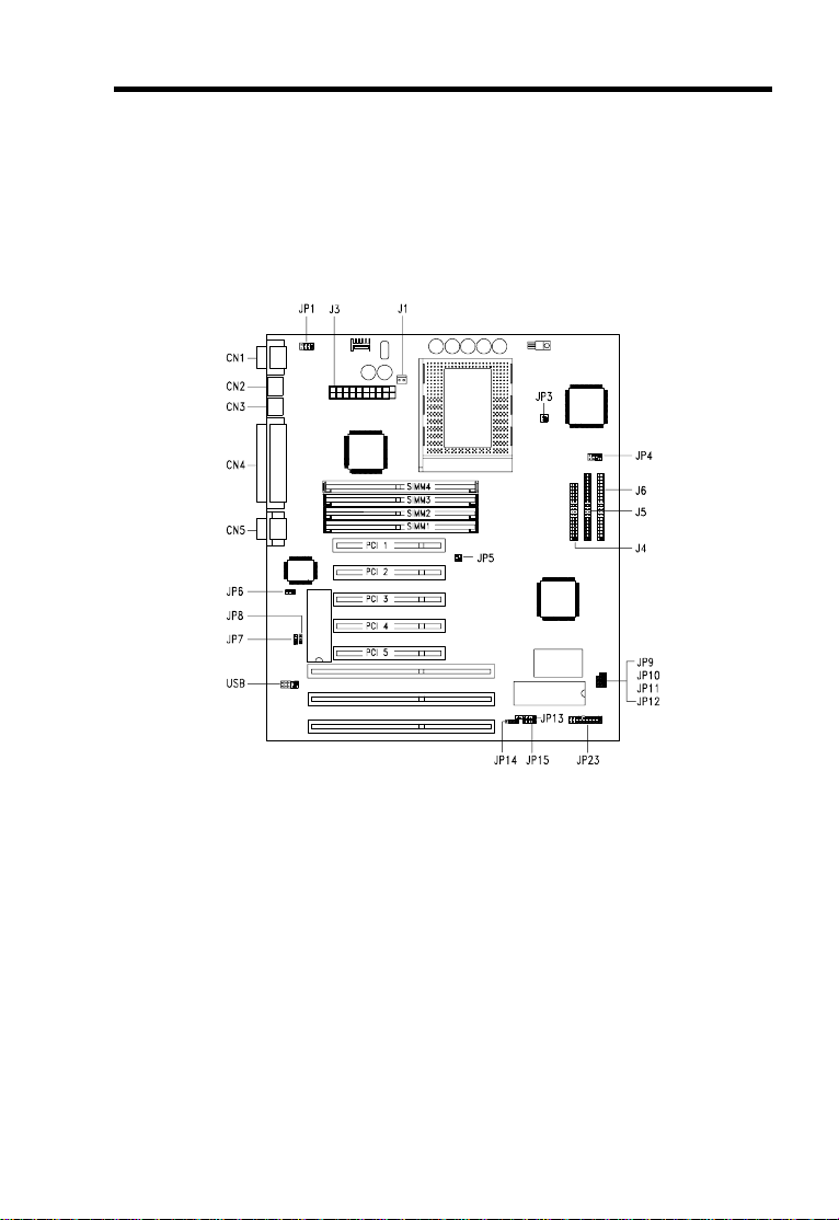
2.2 Jumper and Connector Locations
The following figure shows the locations of the jumpers and connectors on the
system board:
J1: Two-pin fan connector JP3 and JP5: CPU external freq.
J3: ATX power connector select jumper
J4: FDD connector JP4: CPU bus ratio select jumper
J5: Primary IDE connector JP6: Super I/O controller function
J6: Secondary IDE connector jumper
JP13: IrDA connector JP7: Keyboard clock jumper
JP14: Software power switch jumper JP8: P/2 mouse function jumper
JP15: HDD LED connector JP9: Reserved jumper
JP23: Multifunction connector JP10: CMOS jumper
CN1: COM1 port JP11 and JP12: Intel Flash ROM
CN2: PS/2 mouse connector programming jumper
CN3: PS/2 keyboard connector
CN4: Parallel port
CN5: COM2 port
2-2
Page 3

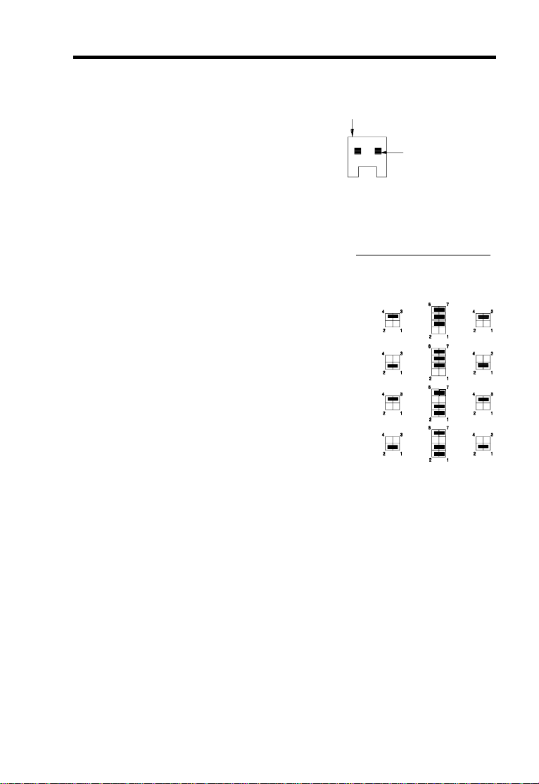
2.3 Setting the Jumper
Set a jumper switch as follows:
• To open a jumper, remove the
jumper cap.
• To close a jumper, insert the
plastic jumper cap over two pins of
a jumper.
The conventions in the figure are used
to represent the proper jumper settings.
Hardware Installation
Open
Closed (1-2)
2-3
Page 4
Hardware Installation
2.4 Installing a Microprocessor
The motherboard comes with a ZIF microprocessor socket that allows you to
install a CPU without using any tool.
Follow these steps to install a CPU into a ZIF-type CPU socket:
Make sure that the system power is OFF before
installing a component.
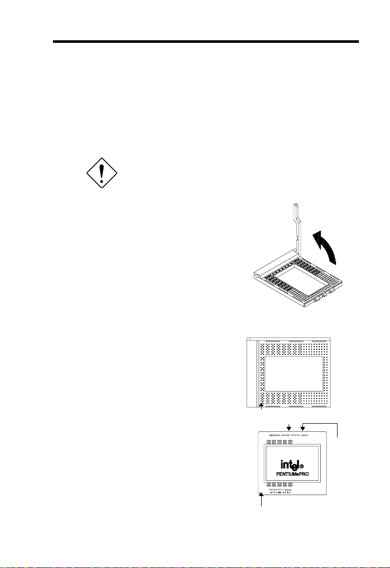
1. Locate the CPU socket on the
system board and pull up the
socket lever.
2. Align pin 1 of the CPU with hole 1
of the socket. The dot on the CPU
indicates pin 1. The topmost label
indicates the CPU frequency and
the cache size.
2-4
Hole 1 CPU frequency
L2 cache
size
supported
Pin 1 indicator
Page 5
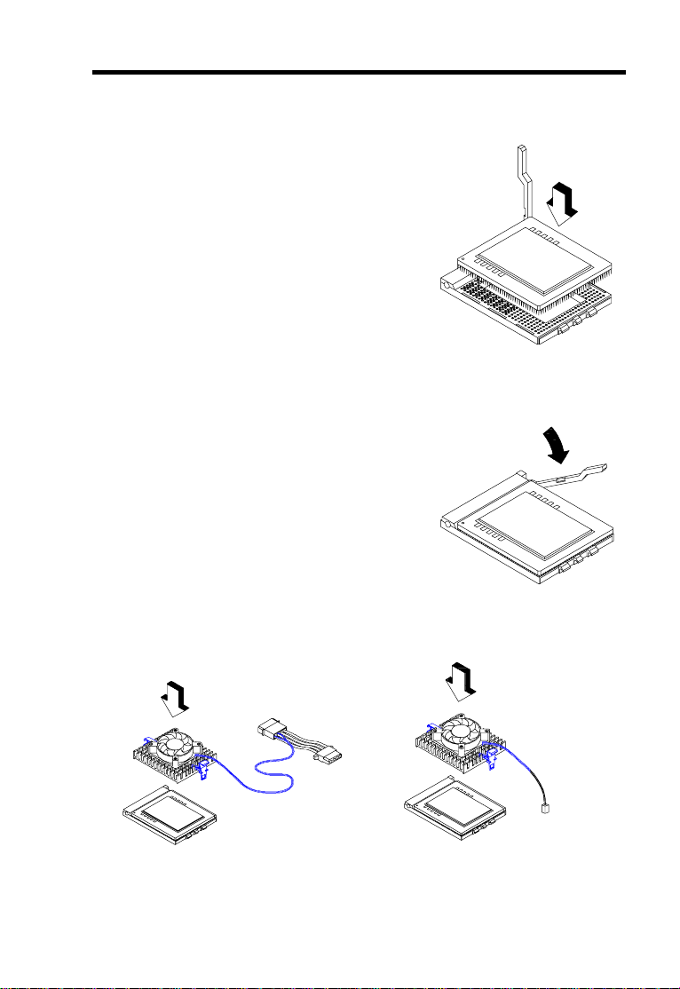
3. Gently insert the CPU into the
socket.
4. Pull down the socket lever to lock
the CPU into the socket.
Hardware Installation
5. Attach the heatsink and fan to the CPU.
With four-pin fan connector
With two-pin fan connector
2-5
Page 6
Hardware Installation
6. Plug in the fan cable to the two-pin
+12V
fan connector onboard. The fan
connector is marked J1 on the
system board. If your fan cable
has four pins, plug it into the
connector on the power supply
2-pin fan power connector (J2)
unit.
7. Set jumpers JP3, JP4 and JP5
CPU FREQUENCY SELECT
according to the frequency
supported by the CPU currently
JP3 JP4 JP5
installed on your board.
150 MHz
166 MHz
180 MHz
200 MHz
2.5 Upgrading the Microprocessor
GND
GND
To upgrade a CPU:
1. Turn off the system power and remove the housing cover.
2. Locate the CPU socket on the system board.
3. Pull up the socket lever.
4. Remove the installed CPU, if any.
5. Install the upgrade CPU. Refer to section 2.4 for instructions on how to
install a CPU.
2-6
Page 7

Hardware Installation
2.6 Configuring the System Memory
The system memory is expandable to 512 MB by adding single in-line
memory modules (SIMMs). The four 72-pin SIMM sockets accommodate
4-, 16- and 64-MB single-density SIMMs, and 8- and 32-MB double-density
SIMMs. These SIMM sockets also accept both FPM and EDO type DRAMs,
with or without parity. The EDO feature extends the data transfer cycle, thus
improves memory performance. All SIMMs support a DRAM speed of 60/70
ns or less.
The SIMMs with parity supports the ECC (Error Checking and Correction)
feature that enables the system to detect and correct data errors. To fully
support this function, you must install 36-bit parity-type SIMMs (i.e., 8 chips
plus 4 parity chips) in pairs in all banks. The combination of 32-bit non-parity
(i.e., 8 chips) and 36-bit parity-type (i.e., 12 chips) memory configuration is
also possible; however, this does not allow you to make use of the ECC
function.
The following are the possible SIMM configurations. Notice that you must
install the same SIMMs in one bank.
Memory Configurations
Bank 0 Bank 1 Total
SIMM 1 SIMM 2 SIMM 3 SIMM 4 Memory
4 MB 4 MB 8 MB
4 MB 4 MB 4 MB 4 MB 16 MB
8 MB 8 MB 16 MB
8 MB 8 MB 4 MB 4 MB 24 MB
8 MB 8 MB 8 MB 8 MB 32 MB
16 MB 16 MB 32 MB
2-7
Page 8

Hardware Installation
Memory Configurations (continued)
Bank 0 Bank 1 Total
SIMM 1 SIMM 2 SIMM 3 SIMM 4 Memory
4 MB 4 MB 16 MB 16 MB 40 MB
8 MB 8 MB 16 MB 16 MB 48 MB
16 MB 16 MB 16 MB 16 MB 64 MB
32 MB 32 MB 64 MB
4 MB 4 MB 32 MB 32 MB 72 MB
8 MB 8 MB 32 MB 32 MB 80 MB
16 MB 16 MB 32 MB 32 MB 96 MB
32 MB 32 MB 32 MB 32 MB 128 MB
64 MB 64 MB 128 MB
4 MB 4 MB 64 MB 64 MB 136 MB
8 MB 8 MB 64 MB 64 MB 144 MB
16 MB 16 MB 64 MB 64 MB 160 MB
32 MB 32 MB 64 MB 64 MB 192 MB
64 MB 64 MB 64 MB 64 MB 256 MB
128 MB 128 MB 256 MB
4 MB 4 MB 128 MB 128 MB 264 MB
8 MB 8 MB 128 MB 128 MB 272 MB
16 MB 16 MB 128 MB 128 MB 288 MB
32 MB 32 MB 128 MB 128 MB 320 MB
64 MB 64 MB 128 MB 128 MB 384 MB
128 MB 128 MB 128 MB 128 MB 512 MB
2-8
Make sure that you install the same SIMM type for each
bank.
Do not install memory modules that contain more than
24 chips. These modules exceed the ASIC
specification. Doing so may result in unstable system
performance.
Page 9

2.6.1 Installing a SIMM
Observe the ESD precautions when installing
components.
Follow these steps to install a SIMM:
1. Slip a SIMM at a 45 ° angle into a
socket. If the SIMM does not
completely fit into the socket,
reverse the SIMM orientation. The
SIMM has a curved edge indicating
pin 1 that ensures installation in
one direction only.
Be careful when inserting or removing SIMMs.
Forcing a SIMM in or out of a socket can
damage the socket or the SIMM (or both).
Hardware Installation
curved edge
2. Gently push the SIMM up until the
pegs of the socket slip into the
holes on the SIMM and the holding
clips lock the SIMM into a vertical
position.
The SIMM should be at a 90 angle when
installed.
2-9
Page 10

Hardware Installation
2.6.2 Removing a SIMM
To remove a SIMM:
1. Press the holding clips on both
sides of the SIMM outward to
release it.
2. Press the SIMM downward to
about a 45° angle.
3. Gently pull the SIMM out of the
socket.
2-10
Page 11

Hardware Installation
2.7 Customizing your Hardware Setup
You may customize your hardware setup according to your desired system
performance. However, doing so requires resetting of several jumpers. The
onboard jumpers are normally set to its default setting. See the figure in
section 2.2 for the location of the jumpers on the system board.
The following sections tell how to configure the system board to meet the
desired performance:
2.7.1 Setting the Voltage Regulator
The jumper JP1 enables you to set the voltage of the onboard voltage
regulator. The supported voltage range is from 2.1V to 3.5V. See the
following figure for the correct settings.
Voltage JP1 Voltage JP1
*
Auto *
3.5V
3.4V
3.3V
3.2V
3.1V
3.0V
2.9V
* The system can automatically detect the CPU volltage through the VID pins; therefore,
by default, JP1 is set to OPEN. You do not need to set the voltage regulator setting.
2.8V
2.7V
2.6V
2.5V
2.4V
2.3V
2.2V
2.1V
2-11
Page 12

Hardware Installation
2.7.2 Disabling the Onboard Super I/O Controller
The board is preset by the manufacturer
with the onboard I/O controller enabled.
In case you wish to use an external I/O
controller, you need to disable the
onboard I/O before the external I/O card
functions. To disable, you need to reset
jumper JP6 to 1-2.
Enabled
Disabled
2.7.3 Setting the Keyboard Clock
By default, the keyboard clock is set
according to the ISA clock. If you want
to increase the clock setting to 12 MHz
by simply resetting jumper JP7 to 1-2.
JP7
2.7.4 Disabling the PS/2 Mouse Function
JP6
ISA Clock
12 MHz
The PS/2 mouse function is normally
enabled and occupies IRQ12. To
reassign IRQ12 to another function, you
need to disable the PS/2 mouse function
by setting jumper JP8 2-3 and changing
the BIOS setting (see Chapter 3).
2-12
JP8
Enabled
Disabled
Page 13

Hardware Installation
2.7.5 Enabling the Intel Flash ROM Boot Block
Programming
The Intel Flash ROM has two areas that
can be programmed separately: the
8KB boot block and the 120KB main
BIOS area.
The jumpers JP11 and JP12 allow you
to program the Flash ROM boot block.
By default, the boot block program
function is enabled and both JP11 and
JP12 are set to 1-2.
Enabled (default)
Reserved
The jumper setting shown above applies only
for Intel Flash ROM.
Do not change the default setting of JP11
and JP12. Doing so modifies the main BIOS
area but not the boot block, causing the
BIOS to become inconsistent. This may
result in serious system damage.
2.7.6 Selecting the Power Switch Type
The jumper JP14 allows you to set the
power switch type that you want to
support, i.e., either the toggle type or the
momentary type. However, before you
set this jumper, make sure that you
know your power switch type.
JP14
Toggle type switch
Momentary type switch
JP11 JP12
2-13
Page 14

Hardware Installation
To differentiate a toggle type from a momentary type, check the On and Off
switch position. In a toggle type switch, a pressed switch indicates On
position while a normal switch position indicates Off. In a momentary type,
the switch position does not change for both modes.
To support a toggle type switch, close pins 2-3 of JP14. Close all pins (1-4)
to support a momentary type switch.
2.7.7 Clearing the CMOS
You need to clear the CMOS if you forget your system password. To clear the
CMOS, do the following steps:
Before you proceed, check your onboard CMOS
chip. The learing procedures vary depending
on the CMOS chip type. Read the CMOS chip
label to determine the chip type.
For Dallas DS12887A:
1. Turn off the system power.
2. Locate JP10 and short pins 1-2 for
a few seconds. Check your manual
for the correct jumper settings and
location of the jumpers.
3. Reset JP10 to its normal setting by
shorting pins 2-3.
4. Turn on the system power.
5. Press
the BIOS Setup Utility and specify a
new password, if needed.
during bootup to enter
Normal (default)
Clear CMOS
JP10
2-14
Page 15

Hardware Installation
For Dallas DS12B887, BENCHMARQ bq3287AMT, or SGS ST M48T86 PCI
chip:
1. Turn off the system power.
2. Locate JP10 and short pins 1-2 for a few seconds. Check your manual
for the correct jumper settings and location of the jumpers.
3. Turn on the system power.
4. Turn off the system power again.
5. Reset JP10 to its normal setting by shorting pins 2-3.
6. Turn on the system power .
7. Press
new password, if needed.
during bootup to enter the BIOS Setup Utility and specify a
2-15
Page 16

Hardware Installation
2.8 Installing the System Board
Make sure that you have already installed the
system board components like the CPU and
memory, and have set the appropriate jumpers
before you proceed.
Follow these steps to install a system board into a housing:
1. Open the system housing. Refer
to the housing documentation for
steps on how to remove the
housing cover.
2. Install the board into the housing
and secure it with the screws that
come with the housing.
3. Attach the cables and install the
necessary peripherals. See the
following section for information on
how to connect the peripherals.
2-16
Refer to your housing documentation for more
information on the system housing.
Page 17

Hardware Installation
2.9 Connecting Peripherals
2.9.1 Power Cable
The board comes with an ATX type
power connector. This connector has a
ool-proof design that allows you to
connect the ATX power cable in one
direction only.
If you cannot insert the cable into the
connector, reverse the cable orientation.
Do not force to insert the cable.
The power connector is marked J3 on
the system board.
Make sure that the power supply is off before
connecting or disconnecting the power cable.
2-17
Page 18

Hardware Installation
2.9.2 Mouse
PS/2 Mouse
To connect a PS/2 mouse, simply plug
in the PS/2 mouse cable connector to
CN2 on the system board.
Serial Mouse
To connect a serial mouse, plug in the mouse cable connector to CN1
(COM1) or CN5 (COM2). See section 2.9.4.
2.9.3 USB Devices
You need a USB bracket to enable your
system to support USB device(s). To
attach a USB bracket, simply insert the
bracket connector to the onboard USB
connector. See section 2.2 for the
location of the USB connector.
2-18
Page 19

Hardware Installation
2.9.4 Serial Devices (COM1/COM2)
To support serial devices, insert the
serial device connectors to the
appropriate COM ports marked CN1
(COM1) and CN5 (COM2) on the
system board.
2.9.5 Floppy Disk Drives
Connect the drive cable to the floppy
disk drive connector marked J4 on the
system board. See section 2.2 for the
location of the connector. Refer to the
figure on how to connect the cables.
2.9.6 Printer
Plug in the printer cable to the onboard
parallel connector marked CN4. Refer
to the figure.
2-19
Page 20

Hardware Installation
2.9.7 IDE Devices
Primary IDE Connector
The primary IDE connector marked J5
on the system board supports two IDE
devices - one IDE hard disk and one
additional IDE device. Connect your
IDE HDD to the master port of the
primary IDE cable. If you have other
IDE device to install in your system,
connect it to the slave port.
Secondary IDE Connector
The secondary IDE connector is marked
J6 on the board. This connector also
supports two IDE devices. To install an
IDE CD-ROM drive into your system,
insert master port of the secondary IDE
cable into the CD-ROM drive connector.
If you have more than two hard disks,
connect your third hard disk to the
master port of the cable. Then, connect
your CD-ROM drive to the slave port.
HDD 1
Master port
HDD 2
Slave port
Master port
Slave port
2-20
Page 21

Hardware Installation
2.9.8 Front-panel Switches and LEDs
HDD LED
The HDD LED connector is marked
JP15 on the board. Plug in the HDD
LED cable to this four-pin connector.
See the figure.
Multifunction Connector
The multifunction connector is a 20-pin
connector marked JP23 on the board.
Attach the green mode LED, software
power switch, reset switch, break switch,
and speaker connectors to its
corresponding pins on the connector as
shown in the figure.
2.9.9 Keyboard
To connect a PS/2 keyboard, plug in the
PS/2 keyboard cable to the PS/2
keyboard connector marked CN3 on the
system board .
Speaker Power LED Keylock
Break Switch Green Mode LEDReset
( Turbo Switch ) ( Turbo LED )
Software Power
wi
h
2-21
Page 22

Hardware Installation
2.9.10 IrDA Module
The connector marked JP13 allows you to install an Infrared (IrDA) module.
The IrDA module enables the system to transfer data and communicate with
portable devices such as laptops, PDA, and printers, without the need to
connect cables. This remote (or wireless) communication function complies
with the IrDA specification, i.e, 115 Kbs maximum data transfer rate at a
distance of up to one meter. The ASK-IR feature is also supported.
When installing an IrDA module, take note of the pin configuration of JP13 to
ensure proper connection.
2-22
Page 23

Hardware Installation
2.10 Installing Expansion Boards
Before you install any expansion board, make sure that you have secured the
system board in the housing.
Follow these steps to install an expansion board:
1. Observe the ESD precautions
before removing the expansion
board from its protective
packaging.
2. Locate an empty expansion slot on
the system board.
3. Remove the bracket opposi te the
slot that you want to use. Save the
cover and screw for future use.
4. Remove the board from its
protective packaging.
Golden edge
ISA slot
5. Gently insert the golden edge of
the board onto the slot until it fits
into place.
6. Secure the bracket to the housing
with a screw.
Golden edge
PCI slot
2-23
 Loading...