

Page 1
18.5″&21.5″&24″ TV Monitor AOC T942we&T2242we&T2442e
Service
Service
Service
Description Page Description Page
Table of Contents.......……....................................…........1
Important Safety Notice.......................................……......2
Revision List…………………………………………………3
1. General Specification..............................……...…........4
2. Operating Instructions………………...…….……….......5
2.1 The Use of Remote Control…….…..……….…….......5
2.2 To Use the Menus….....………………….…..…….......6
2.3 How to Connect……..……………….…….……….....13
2.4 Front Panel Control Knobs…….………….……….....16
3. Input/Output Specification…………....................…....18
4. Mechanical Instructions…………………….................22
5. Repair Flow Chart ……………………….…….…….....29
6. PCB Layout ………………..…………………....….......36
ANY PERSON ATTEMPTING TO SERVICE THIS CHASSIS MUST FAMILIARIZE HIMSELF WITH THE CHASSIS
TABLE OF CONTENTS
6.1 Main Board…………..……………...…….…….......36
6.2 Power Board………………..…….…….……….......40
6.3 Key Board………………………..……..……….......46
6.4 IR Board………………………….……..……….......46
7. Adjustment……..………………………….................47
8. Block Diagram.…….................................................48
9. Schematic Diagram…..…………....………………...50
9.1 Main Board…………………………………...….......50
9.2 Power Board…………..….….……...………….......70
9.3 Key Board……………….……….…………….........74
9.4 IR Board……...………….……….…………….........75
10. Exploded View………………………………….…...76
11. BOM List……………….………………….………….79
SAFETY NOTICE
AND BE AWARE OF THE NECESSARY SAFETY PRECAUTIONS TO BE USED WHEN SERVICING
ELECTRONIC EQUIPMENT CONTAINING HIGH VOLTAGES.
CAUTION: USE A SEPARATE ISOLATION TRANSFOMER FOR THIS UNIT WHEN SERVICING
1
Page 2

Important Safety Notice
Proper service and repair is important to the safe, reliable operation of all AOC Company Equipment. The service
procedures recommended by AOC and described in this service manual are effective methods of performing service
operations. Some of these service operations require the use of tools specially designed for the purpose. The
special tools should be used when and as recommended.
It is important to note that this manual contains various CAUTIONS and NOTICES which should be carefully read in
order to minimize the risk of personal injury to service personnel. The possibility exists that improper service
methods may damage the equipment. It is also important to understand that these CAUTIONS and NOTICES ARE
NOT EXHAUSTIVE. AOC could not possibly know, evaluate and advise the service trade of all conceivable ways in
which service might be done or of the possible hazardous consequences of each way. Consequently, AOC has not
undertaken any such broad evaluation. Accordingly, a servicer who uses a service procedure or tool which is not
recommended by AOC must first satisfy himself thoroughly that neither his safety nor the safe operation of the
equipment will be jeopardized by the service method selected.
Hereafter throughout this manual, AOC Company will be referred to as AOC.
WARNING
Use of substitute replacement parts, which do not have the same, specified safety characteristics might create
shock, fire, or other hazards.
Under no circumstances should the original design be modified or altered without written permission from AOC.
AOC assumes no liability, express or implied, arising out of any unauthorized modification of design.
Servicer assumes all liability.
FOR PRODUCTS CONTAINING LASER:
DANGER-Invisible laser radiations when open AVOID DIRECT EXPOSURE TO BEAM.
CAUTION-Use of controls or adjustments or performance of procedures other than those specified herein may
result in hazardous radiation exposure.
CAUTION -The use of optical instruments with this product will increase eye hazard.
TO ENSURE THE CONTINUED RELIABILITY OF THIS PRODUCT, USE ONLY ORIGINAL MANUFACTURER'S
REPLACEMENT PARTS, WHICH ARE LISTED WITH THEIR PART NUMBERS IN THE PARTS LIST SECTION OF
THIS SERVICE MANUAL.
Take care during handling the LCD module with backlight unit
-Must mount the module using mounting holes arranged in four corners.
-Do not press on the panel, edge of the frame strongly or electric shock as this will result in damage to the screen.
-Do not scratch or press on the panel with any sharp objects, such as pencil or pen as this may result in damage to
the panel.
-Protect the module from the ESD as it may damage the electronic circuit (C-MOS).
-Make certain that treatment person’s body is grounded through wristband.
-Do not leave the module in high temperature and in areas of high humidity for a long time.
-Avoid contact with water as it may a short circuit within the module.
-If the surface of panel becomes dirty, please wipe it off with a soft material. (Cleaning with a dirty or rough cloth may
damage the panel.)
2
Page 3

Revision List
Note: Check updating contents, please input keywords in the “Find box” of PDF and click “OK”. After that, it will
automatically locate to the updating contents.
Version Release Date Revision Instructions
A00 Aug.2,2010 Initial Release T2242We V2AAAANSX4K66N
A01 Oct.15,2010 Add new customer model T942We V1BAAANSX4K73N
A02 Dec.9,2010 Add new customer model T2442e V24AAANCX4ACNN
A03 Dec.15,2010 Add new model T2242We V2AAAANCX4ADNN
Add new models,
lead in the new power board[PCB
P/N: 715G3977P04000004L]
A04 Dec.28,2010
A05 Jan.18,2011 Add new models
Update as below:
PCB Layout
Schematic
BOM
Customer
Model
T2242We V2AAAANCX41GNN
T2442e V24AAANCX41GNN
T2242WE V2AAAANCX4PUNN
T2442e V24AAANCX4PUNN
TPV Model
A06 Mar.01,2011 Add the new model T942We V1BAAANSX4K83N
V2AAAANCX4ACNN
T2242WE
A07 May.13,2011 Add new model
T2442e V24AAANCX4A2NN
T2442E V24AAANAX4UNNN
A08 Dec.13,2011 Add new models
T2442E V24AAANCX4GGNN
V2AAAANEX4GGNN
3
Page 4
1. General Specification
Model T942we T2242we T2442e
Panel size 470mm (18.5”) 546mm (21.5”)
Resolution 1366 x 768 1920 x 1080
View Angle
Brightness 250cd/m² 250cd/m² 250cd/m²
Dynamic Contrast Ration 20,000,000:1 20,000,000:1 20,000,000:1
Speaker 3Wx2 3Wx2 5Wx2
Video System PAL M/N,NTSC M PAL M/N,NTSC M PAL DK/BG/I
Audio System M,N M,N DK/BG/I
Antenna impedance 75Ω 75Ω 75Ω
Input Voltage AC100-240V 50/60Hz AC100-240V 50/60Hz 220V 50/60Hz
Power consumption ≤35W ≤42W ≤45W
Horizontal 170°
Vertical 160°(Typ.)
Horizontal 170°
Vertical 160°(Typ.)
609mm (24”)
1920 x 1080
Horizontal 170°
Vertical 160°(Typ.)
Standby power
consumption
Size(W x H x D)
(with base and stand) (mm)
Wall mount accessory Option Option Option
Mall mount size
Equipment:
Operation Temperature
Operation Humidity
Storage Temperature
Storage Humidity
≤1W ≤1W ≤1W
458 x 367 x 179.4 521x401.5x179.4 581.4 x 435.6 x 194.4
75 x75mm
M4x4 pcs (Screw)
0ºC~40ºC
20~70%
-20ºC~60ºC
5~95%
75 x75mm
M4x4 pcs (Screw)
0ºC~40ºC
20~70%
-20ºC~60ºC
5~95%
100 x 100mm
M4 x 4 pcs (Screw)
0ºC~35ºC
20~80%
-20ºC~50ºC
10~90%
4
Page 5
2. Operating Instructions
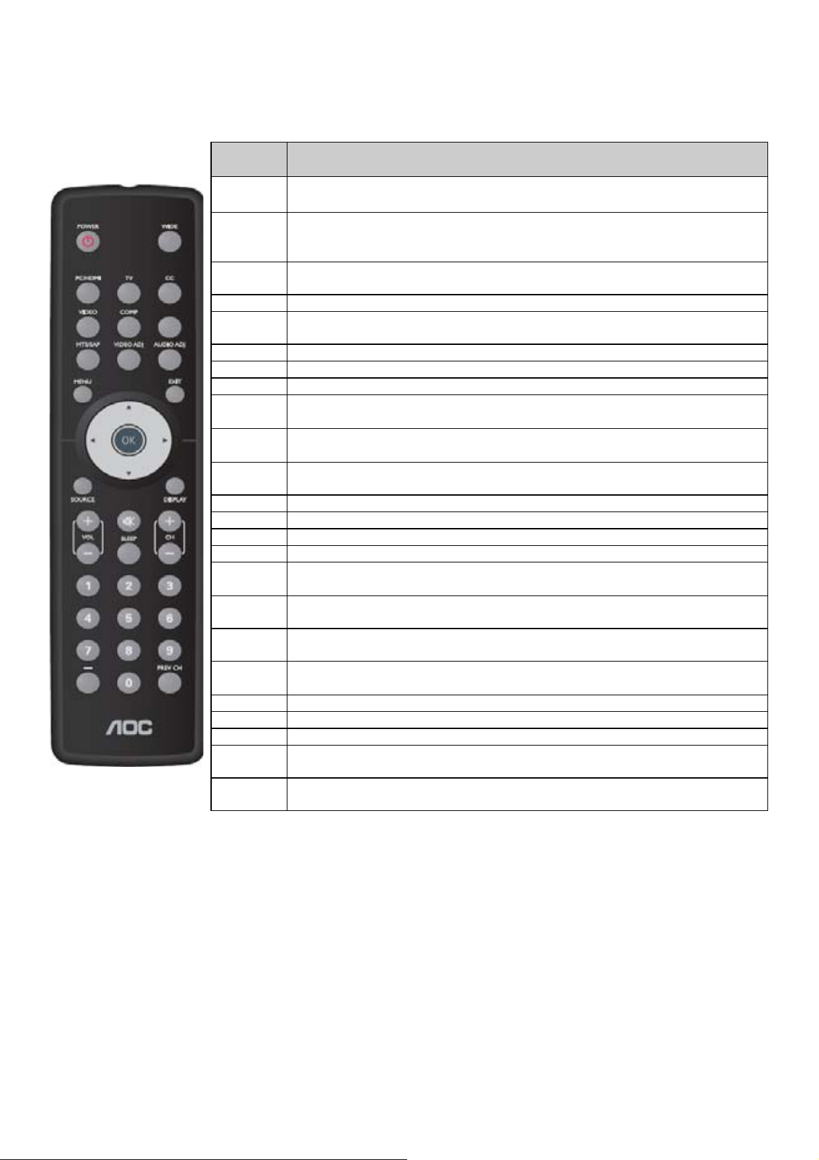
2.1 The Use of Remote Control
Button Description
POWER:
0~9/100
Digit
buttons
DISPLAY
MUTE
CH +/-
VOL+/-
Source
MENU
WIDE
AUDIO
ADJ
VIDEO
ADJ
PC/HDMI
TV
VIDEO
COMP
Up
Down
Left
Right
OK
CC
PREV CH
–
MTS/SAP
Press to turn on/off the TV. The TV is never completely powered off unless it
is physically unplugged. To select a TV channel.
To select a TV channel.
Press this button to display channel number on the left top corner In all
source and display source on the left top corner in the other source
Temporarily interrupt the sound or restore it.
Press CH+ to switch to next channel
Press CH- to switch to last channel
Press + or -to adjust the volume.
Switch your input source(PC/HDMI/AV/S-Video/YPbPr/TV)
Press repeatedly to display OSD menu.
4:3 / 16:9 (non-Linear) / Movie / Panorama
Switch Zoom the video & audio will mute less then 2 sec.
Press this key to select Audio Scenario mode(include Standard, Club,
Dance, Live & Pop)
Switch picture mode(Vivid / Standard / Mild / User)
Select your input source to HDMI or PC
Select your input source to TV source
Select your input source to AV/S-Video source
Select your input source to Component video
Press this key to shift up in the OSD menu
In all source, equal CH+ key
Press this key to shift down in the OSD menu
In all source, equal CH- key
Press this key to shift left in the OSD menu
In all source, equal VOL- key
Press this key to shift right in the OSD menu
In all source, equal VOL+ key
Equal to enter
Closed captioning function
Return last channel
When you skip channel, press this key to replace decimal or centesimal
number
Press this key to activate Multi-channel Television Sound (include Stereo,
Sap and Mono sound)
5
Page 6
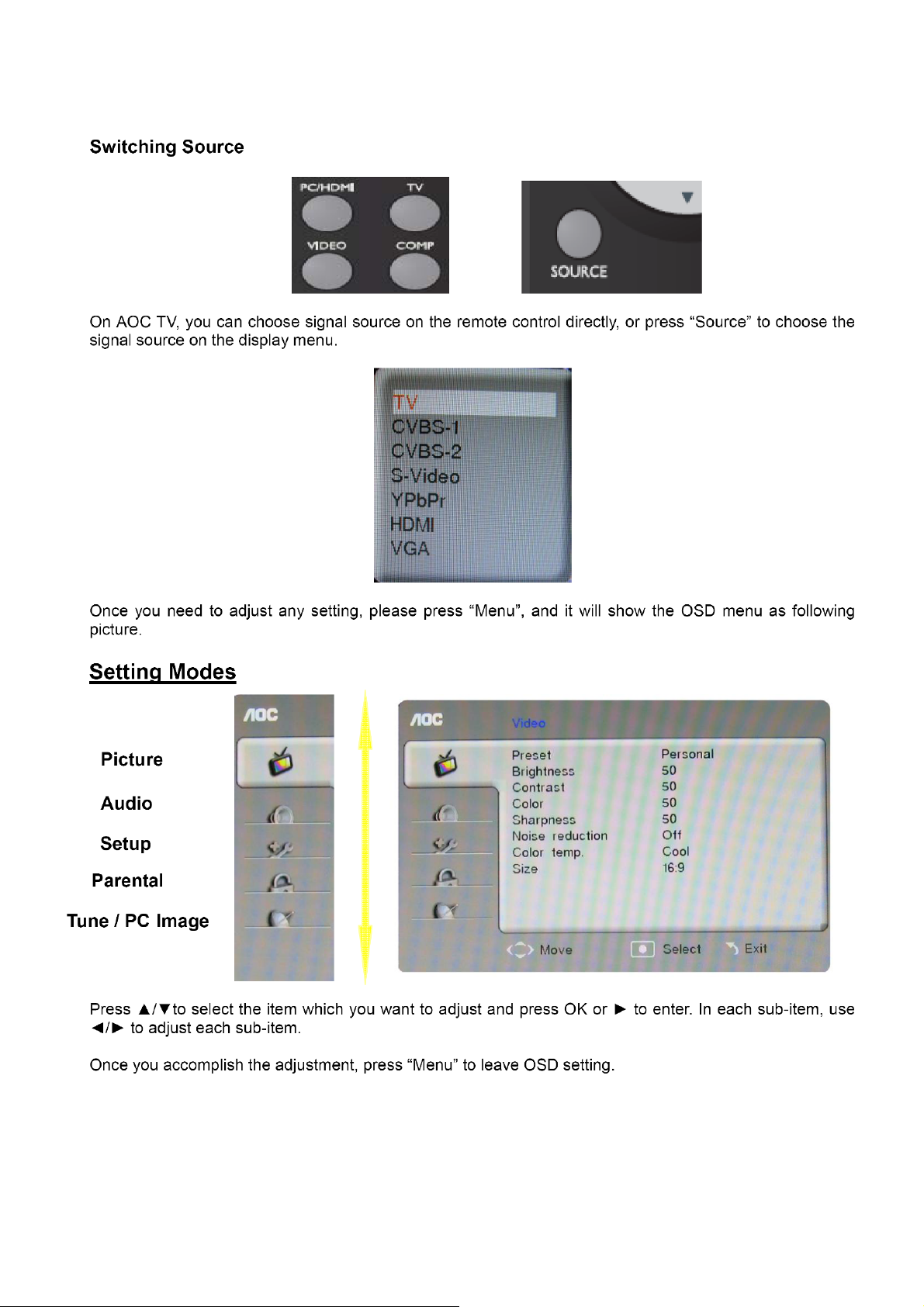
2.2 To Use the Menus
Using TV Features
6
Page 7
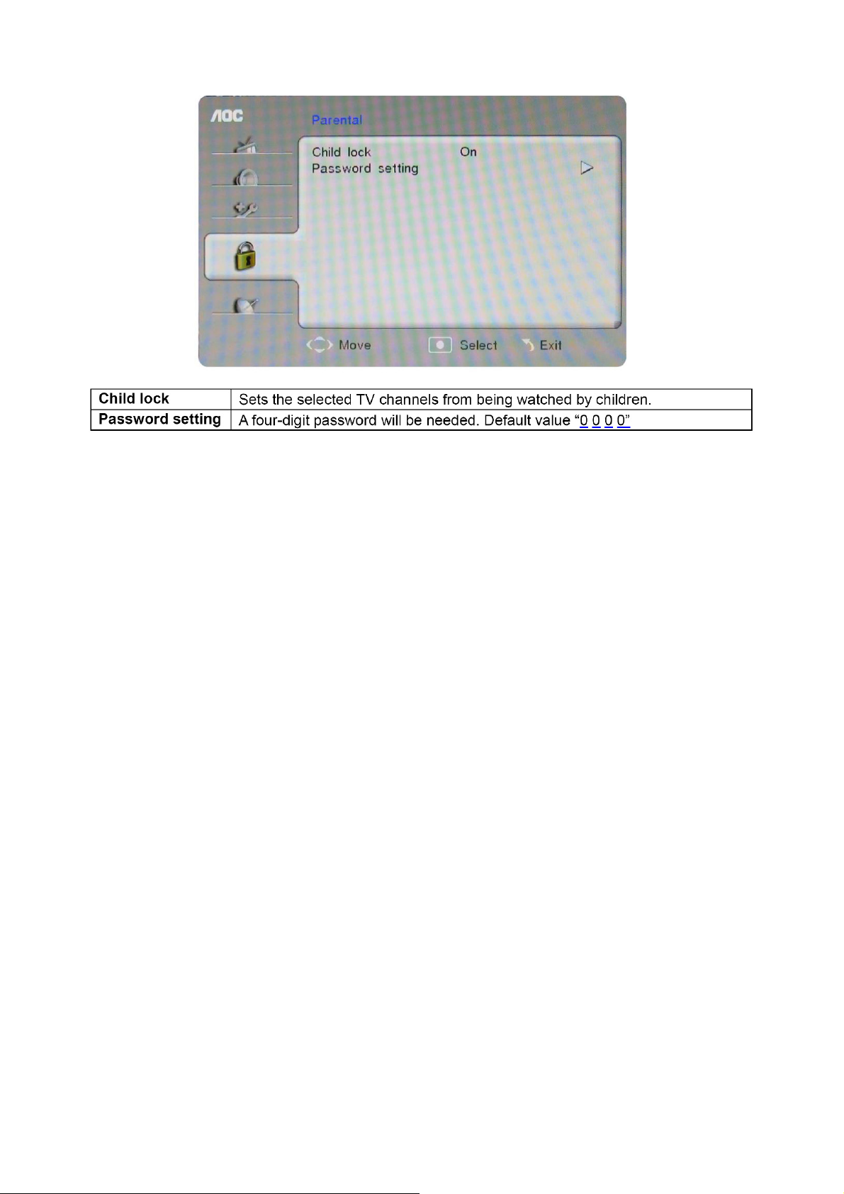
Parental Control Description
7
Page 8
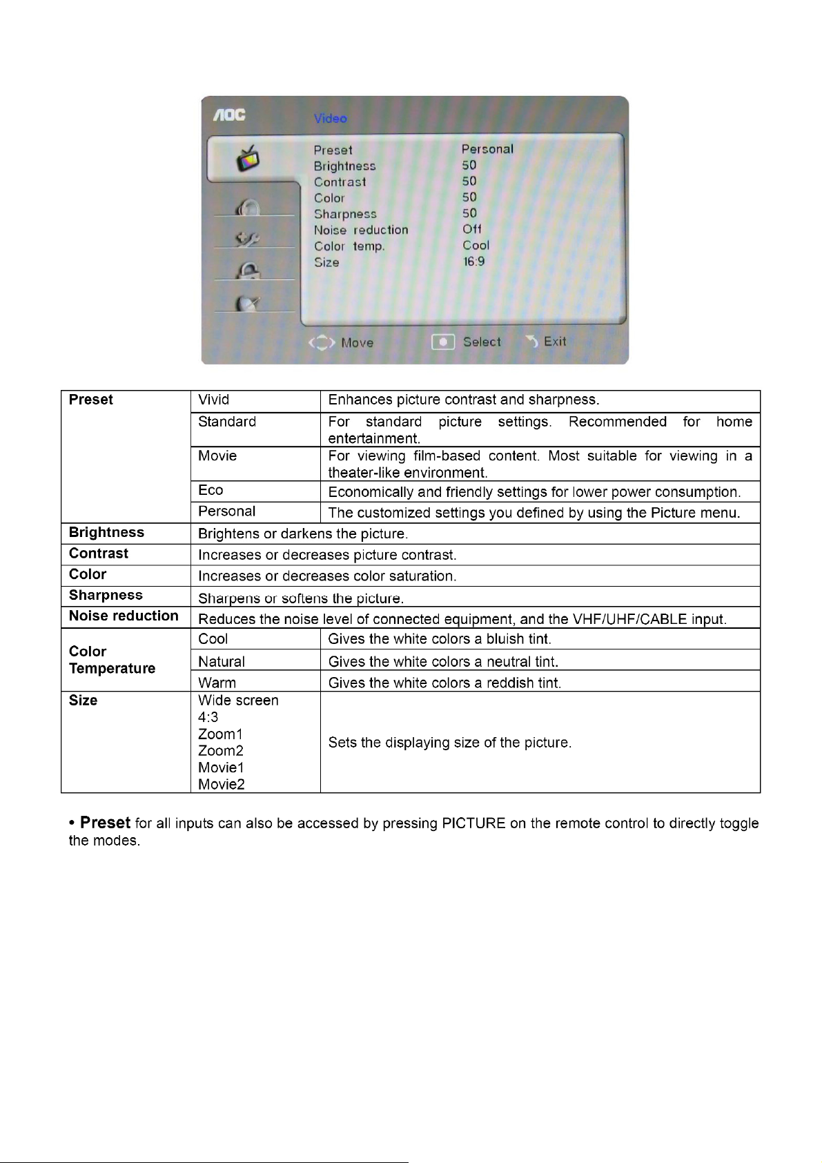
Picture Settings Descriptions
8
Page 9

Audio Settings Descriptions
9
Page 10
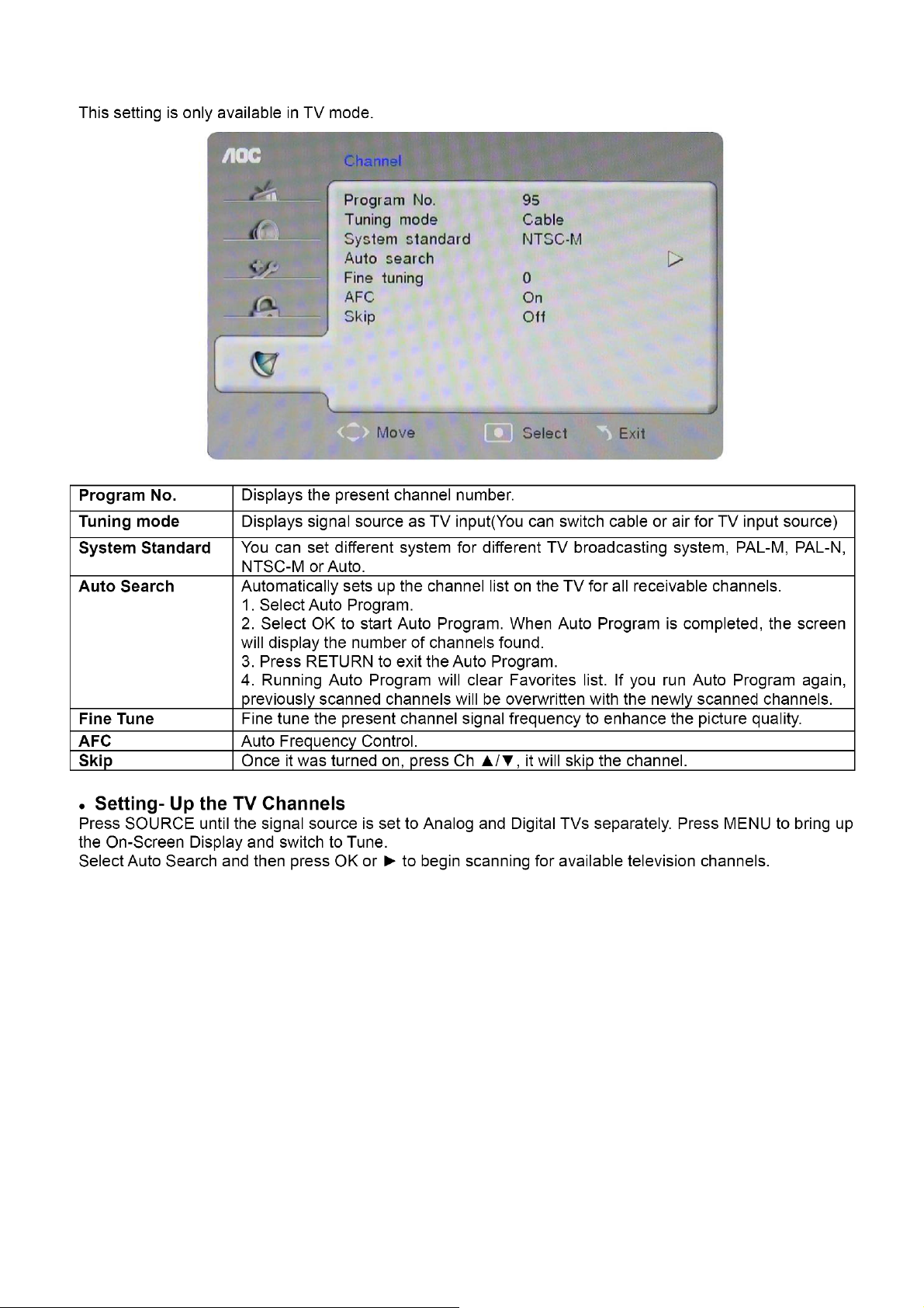
Tune Settings Descriptions
10
Page 11
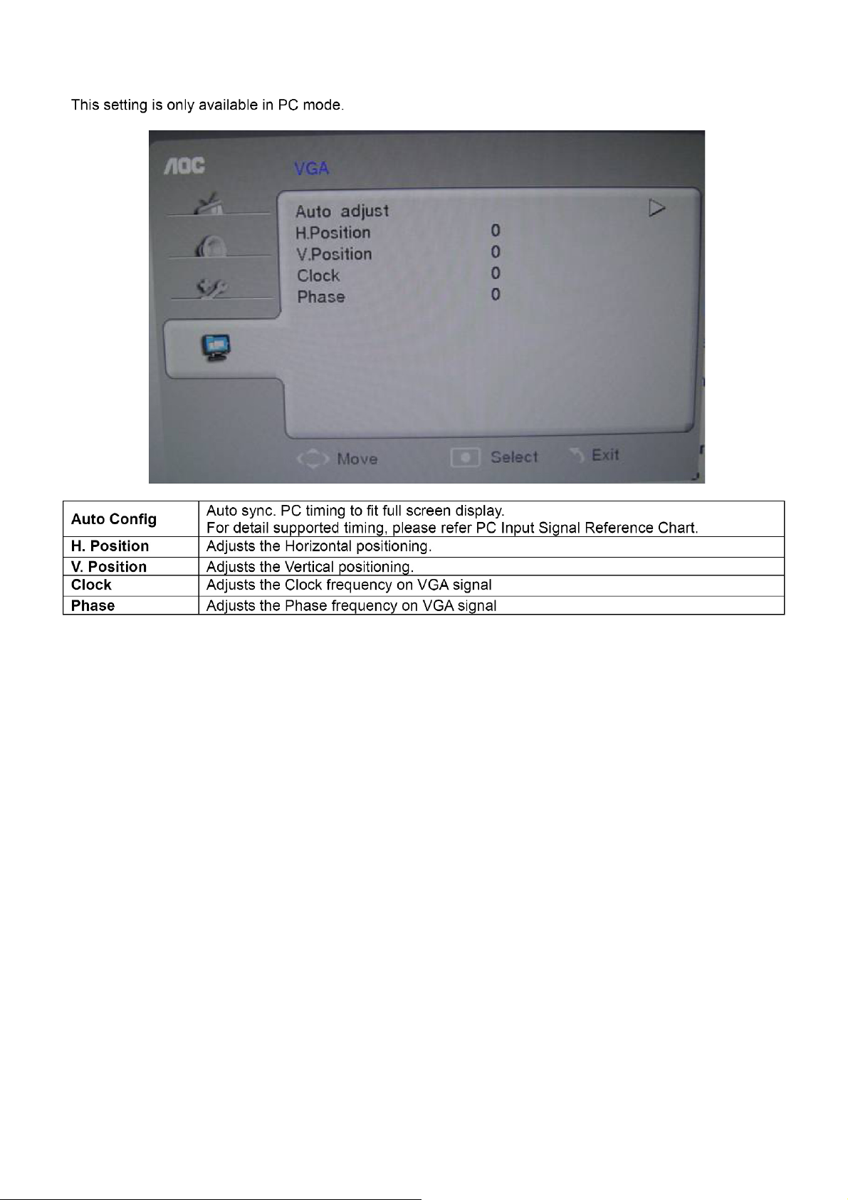
PC Image Settings Descriptions
11
Page 12
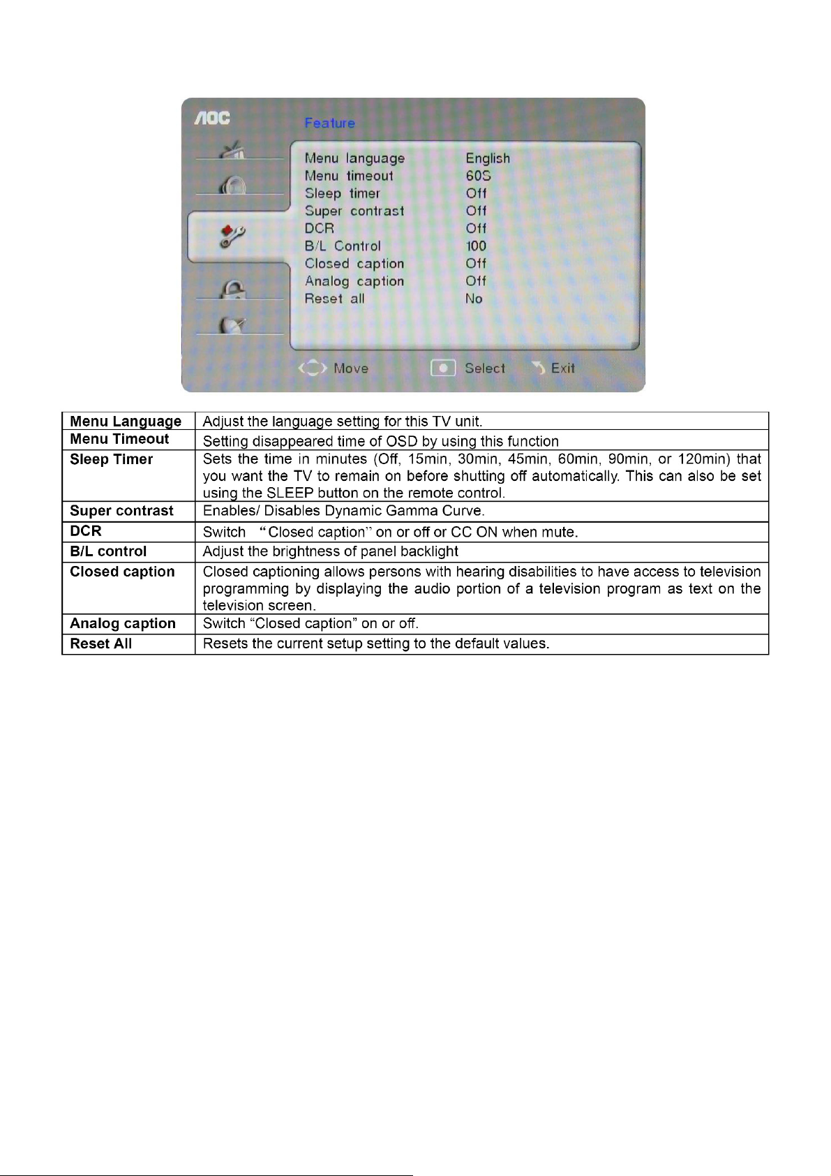
Setup Settings Descriptions
12
Page 13
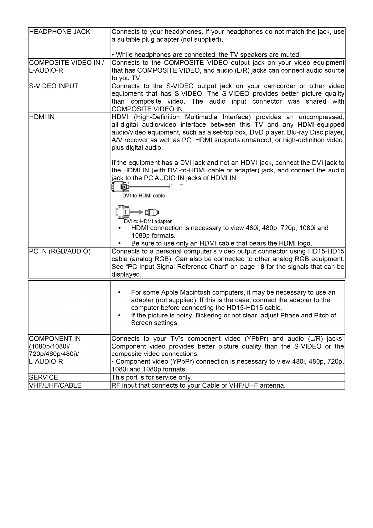
2.3 How to Connect
Connecting TV
13
Page 14
14
Page 15
15
Page 16
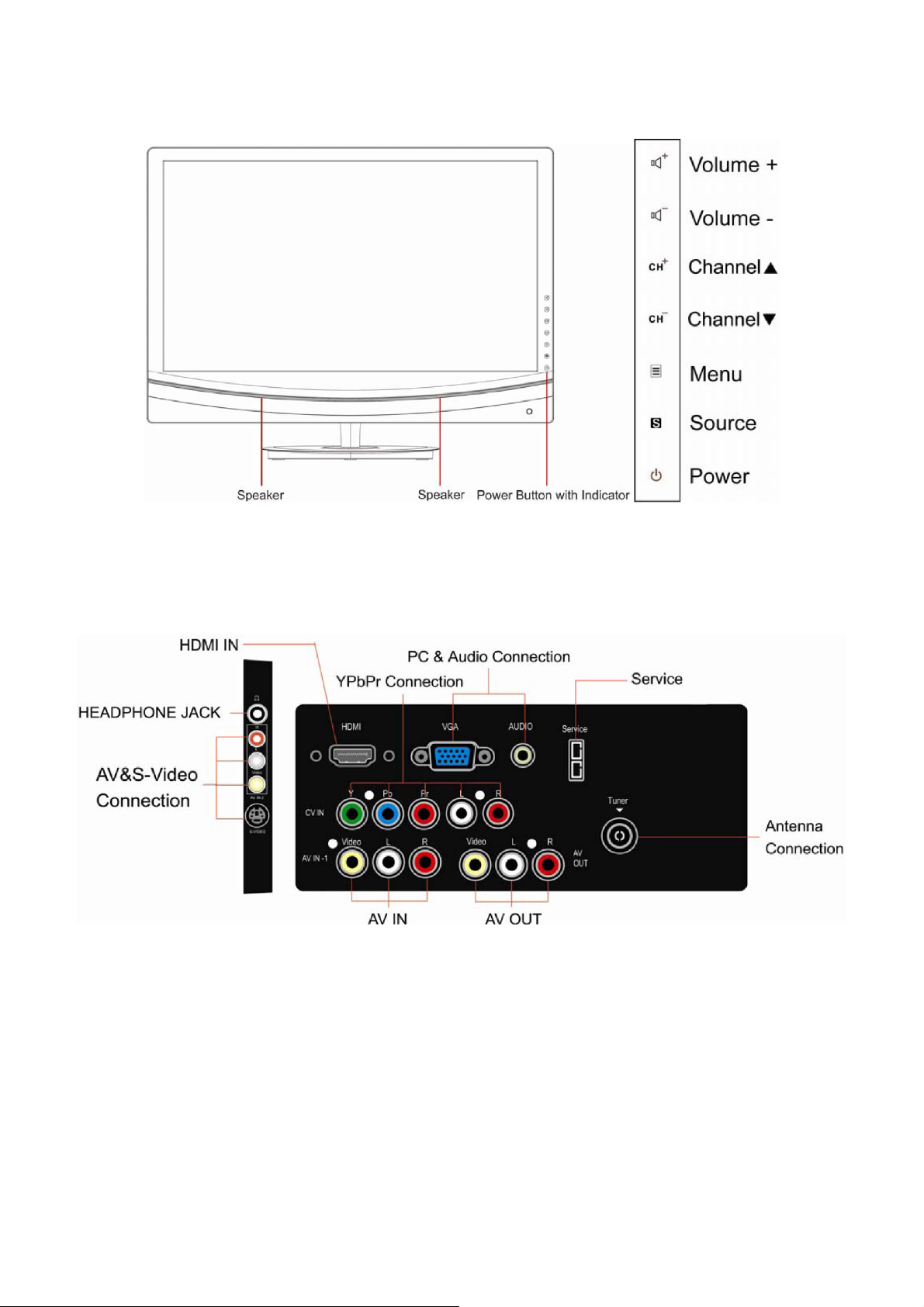
2.4 Front Panel Control Knobs
16
Page 17
17
Page 18
3. Input/Output Specification
3.1 RGB Signal Input
15 - Pin Color Display Signal Cable
Pin No. Description Pin No. Description
1 Red 9 +5V (Supply from PC)
2 Green 10 Sync Ground
3 Blue 11 NC
4 NC 12 Bi-directional data(SDA)
5 Ground 13 H-Sync.
6 Red Ground 14 V-Sync.
7 Green Ground 15 Data clock(SCL)
8 Blue Ground
3.2 HDMI Digital Connector Pin Assignments
Pin No. Description Pin No. Description
1 TMDS Data2+ 2 TMDS Data2 Shield
3 TMDS Data2- 4 TMDS Data1+
5 TMDS Data1 Shield 6 TMDS Data1-
7 TMDS Data0+ 8 TMDS Data0 Shield
9 TMDS Data0- 10 TMDS Clock+
11 TMDS Clock Shield 12 TMDS Clock-
13 CEC 14 Reserved (N.C. on device)
15 SCL 16 SDA
17 DDC/CEC Ground 18 +5V Power
19 Hot Plug Detect
18
Page 19

3.3 Compatible Mode Table
T942We
Resolution
DOS 640x350/70 25.18 31.47 70.09 449 p / n
DOS 720x400/70 28.32 31.47 70.09 449 n / p
DMT 4:3 640x480/60 25.18 31.47 59.94 525 n / n
MAC 640x480/67 30.24 35.00 66.67 525 n / n
DMT 4:3 640x480/72 31.50 37.86 72.81 520 n / n
DMT 4:3 640x480/75 31.50 37.50 75.00 500 n / n
DMT 4:3 640x480/85 36.00 43.27 85.01 509 n / n
DMT 4:3 800x600/56 36.00 35.16 56.25 625 p / p
DMT 4:3 800x600/60 40.00 37.88 60.32 628 p / p
DMT 4:3 800x600/72 50.00 48.08 72.19 666 p / p
DMT 4:3 800x600/75 49.50 46.88 75.00 625 p / p
DMT 4:3 800x600/85 56.25 53.67 85.06 631 p / p
MAC 832x624/75 57.28 47.73 74.55 667 n / n
WVGA 1024X600/60
DMT 4:3 1024x768/60 65.00 48.36 60.00 806 n / n
DMT 4:3 1024x768/70 75.00 56.48 70.07 806 n / n
DMT 4:3 1024x768/75 78.75 60.02 75.03 800 p / p
IBM 1024x768/76 83.10 61.10 76.00 803 p / p
DMT 1024x768/85 94.50 68.68 85.00 808 p / p
1152x864/60 79.90 54.00 60.00 900 p / p
1152x864/70 94.50 63.90 70.00 912 p / p
DMT 1152x864/75 108.00 67.50 75.00 900 p / p
MAC 1152x870/75 100.00 68.68 75.06 915 n / n
SUN 1152x900/66 92.94 61.80 65.95 937 p / p
SUN 1152x900/76 105.56 71.71 76.05 943 p / p
CVT 16:9 1280x720/60 74.50 44.77 59.86 748 n / p
CVT 16:9 1280x720/75 95.75 56.46 74.78 755 n / p
CVT 16:9 1280x720/85 110.25 64.40 84.85 759 n / p
CVT 15:9 1280x768/60 79.50 47.78 59.87 798 n / p
CVT 15:9 1280x768/75 102.25 60.29 74.89 805 n / p
CVT 15:9 1280x768/85 117.50 68.63 84.84 809 n / p
CVT 1280x800/60 83.50 49.70 59.81 831 n / p
CVT 1280x800/75 106.50 62.80 74.93 838 n / p
CVT 1280x800/85 122.50 71.55 84.88 843 n / p
DMT 4:3 1280x960/60 108.00 60.00 60.00 1000 p / p
CVT 4:3 1280x960/75 130.00 75.23 74.86 1005 n / p
DMT 4:3 1280x960/85 148.50 85.94 85.00 1011 p / p
DMT 5:4 1280x1024/60 108.00 63.89 60.02 1066 p / p
SUN 5:4 1280x1024/66 117.00 71.70 67.00 1067 p / p
DOS 5:4 1280x1024/72 130.22 76.00 72.00 1064 p / p
DMT 5:4 1280x1024/75 135.00 79.98 75.03 1066 p / p
SUN 5:4 1280x1024/76 138.01 81.10 76.00 1066 n / n
DMT 5:4 1280x1024/85 157.50 91.15 85.02 1072 p / p
DMT 16:9 1360x768/60 85.50 47.71 60.02 795 p / p
Pixel Rate
( MHz )
Horizontal
( KHz )
Vertical
( Hz )
V_Total
( Line )
Polarity
( H / V )
19
Page 20
CVT 16:9 1360x768/75 109.00 60.29 74.89 805 n / p
CVT 16:9 1366x768/60 85.50 47.71 59.79 798 p / p
CVT 1440x900/60_RB 88.75 55.47 59.90 926 p / n
CVT 1440x900/60 106.50 55.94 59.89 934 n / p
CVT
VDMTREV
DMT 4:3 1600x1200/60 162.00 75.00 60.00 1250 p / p
CVT 16:10 1680x1050/60_RB 119.00 64.67 59.88 1080 p / n
CVT 16:10 1680x1050/60 146.25 65.29 59.95 1089 n / p
CVT 16:9 1920x1080/60_RB 138.50 66.59 59.93 1111 p / n
CVT 16:10 1920x1200/60_RB 154.00 74.04 59.95 1235 p / n
CVT 16:9 1920x1080/60_RB 148.50 67.50 60.00 0 p / p
1440x900/75 136.75 70.64 74.98 942 n / p
1440x900/85 157.00 80.43 84.84 948 n / p
1600x900/60
1600x1000/60
108.00 60.00 60.00
T2242We
Standard Resolution
VGA 640×480 @60Hz DMT 31.469 59.940
VGA 640×480 @67Hz MAC 35.000 66.667
VGA 640×480 @72Hz DMT 37.861 72.809
VGA 640×480 @75Hz DMT 37.500 75.000
Dos-mode 720×400 @70Hz DOS 31.469 70.087
SVGA 800×600 @56Hz DMT 35.156 56.250
SVGA 800×600 @60Hz DMT 37.879 60.317
SVGA 800×600 @72Hz DMT 48.077 72.188
SVGA 800×600 @75Hz DMT 46.875 75.000
SVGA 832×624 @75Hz 49.725 74.500
XGA 1024×768 @60Hz DMT 48.363 60.004
XGA 1024×768 @70Hz DMT 56.476 70.069
XGA 1024×768 @75Hz DMT 60.023 75.029
XGA 1024×768 @75Hz MAC 60.241 74.927
*** 1152×864 @75Hz DMT 67.500 75.000
*** 1280×960 @60Hz DMT 60.000 60.000
SXGA 1280×1024 @60Hz DMT 63.981 60.02
SXGA 1280×1024 @75Hz DMT 79.976 75.025
WXGA+ 1440×900 @60Hz CVT16:10 55.935 59.887
WXGA+ 1440×900 @60Hz RB CVT16:10 55.469 59.901
WSXGA 1680X1050 @60Hz CVT16:10 65.290 59.954
WSXGA 1680X1050 @60Hz RB CVT16:10 64.674 59.883
HD 1920×1080@60Hz 67.500 60.000
SD 480P@60Hz for SDTV Digital only 31.469 59.94
SD 576P@50Hz for SDTV Digital only 31.250 50.000
HD 720P@60Hz for HDTV Digital only 45.000 60.000
HD 720P@50Hz for HDTV Digital only 37.500 50.000
HD 1080i@60Hz for HDTV Digital only 33.750 60.000
HD 1080i@50Hz for HDTV Digital only 28.125 50.000
HD 1080P@60Hz for HDTV Digital only 67.500 60.000
HD 1080P@50Hz for HDTV Digital only 56.250 50.000
Horizontal
Frequency (kHz)
Vertical Frequency
(Hz)
20
Page 21
T2442e
PC Input Signal Reference Table
After connecting the PC to the TV with the VGA port, set the PC output signal according to the table below.
Default PC mode
Standard Resolution H. Sync. (kHz) V. Sync. (kHz)
VESA 640 x 480 31.469 59.940
VESA 800 x 600 37.879 60.317
VESA 1024 x 768 48.363 60.004
VESA 1360 x 768 47.720 59.799
WXGA+ 1400 x 900 59.887 55.935
WSXGA 1680 x 1050 59.884 64.674
FHD 1920 x 1080 60.000 67.500
HDMI Input Signal Reference Table
When connecting the PC to this TV with HDMI, set the PC output signal according to the table below.
Default HDMI mode
Standard Resolution H. Sync. (kHz) V. Sync. (kHz)
VESA 640 x 480 31.469 59.940
VESA 800 x 600 37.879 60.317
VESA 1024 x 768 48.363 60.004
VESA 1360 x 768 47.720 59.799
WXGA+ 1400 x 900 59.887 55.935
WSXGA 1680 x 1050 59.884 64.674
FHD 1920 x 1080 60.000 67.500
Video Input Signal Reference Table
1. After connecting video equipment to this TV with component video or HDMI, set the output signals of the video
equipment according to the table below.
2. If the graphic card of the PC supports video out, you can also set the PC output signals according to the table
below.
Default Component Video or HDMI mode
Standard Resolution H. Sync. (kHz) V. Sync. (kHz)
SD 720 x 480i 15.734 60
SD 720 x 480P 31.500 60
SD 720 x 576i 15.625 50
SD 720 x 576P 31.250 50
HD 1280 x 720P 37.500 50
HD 1280 x 720P 45.000 60
HD 1920 x 1080i 28.125 50
HD 1920 x 1080i 33.750 60
FHD 1920 x 1080P 56.300 50
FHD 1920 x 1080P 67.500 60
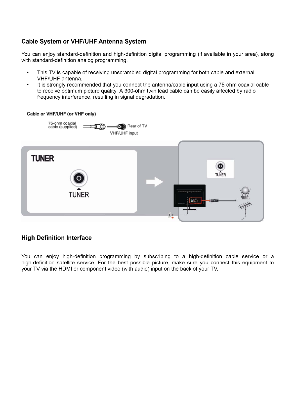
Video Components Supporting TV, Video and S-video
PAL D/K B/G I; NTSC M/N.
HD Interface
You can also play back traditional programs with a DVD player or VCR player by connecting these video
components to the TV from the video or S-video terminals on the side of the TV.
21
Page 22
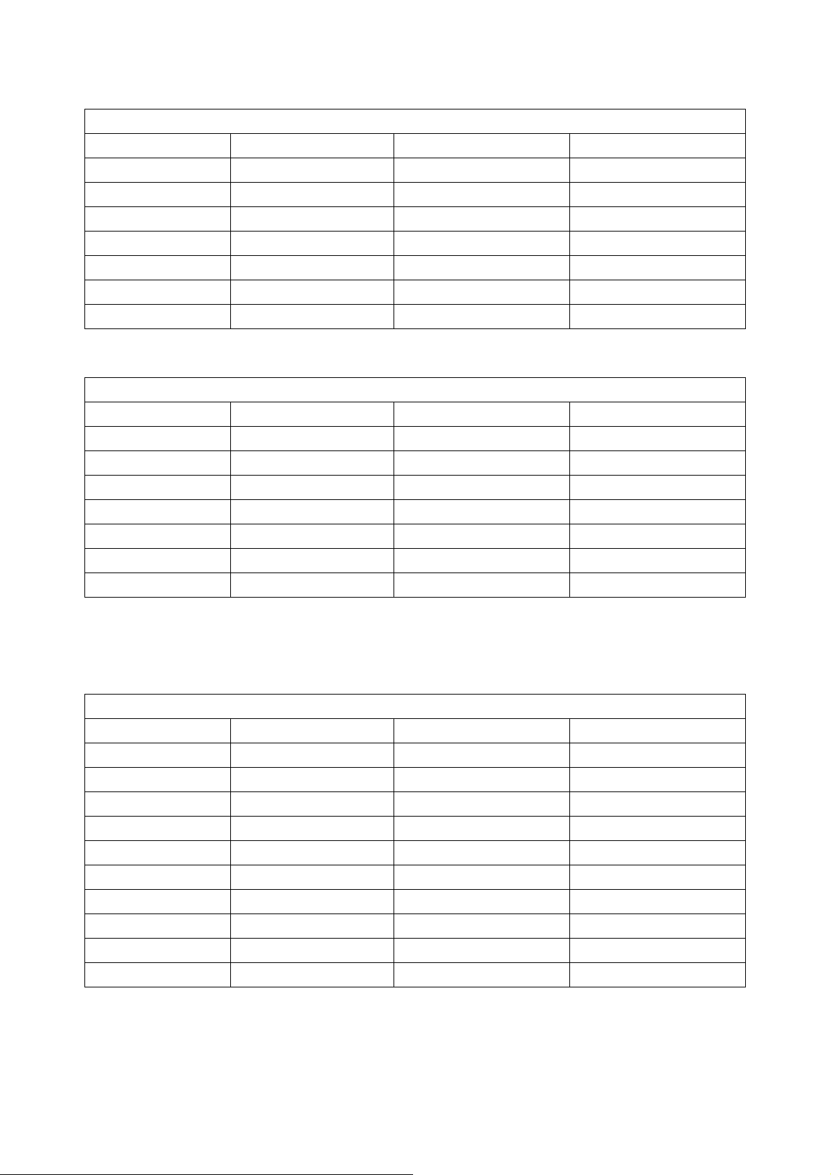
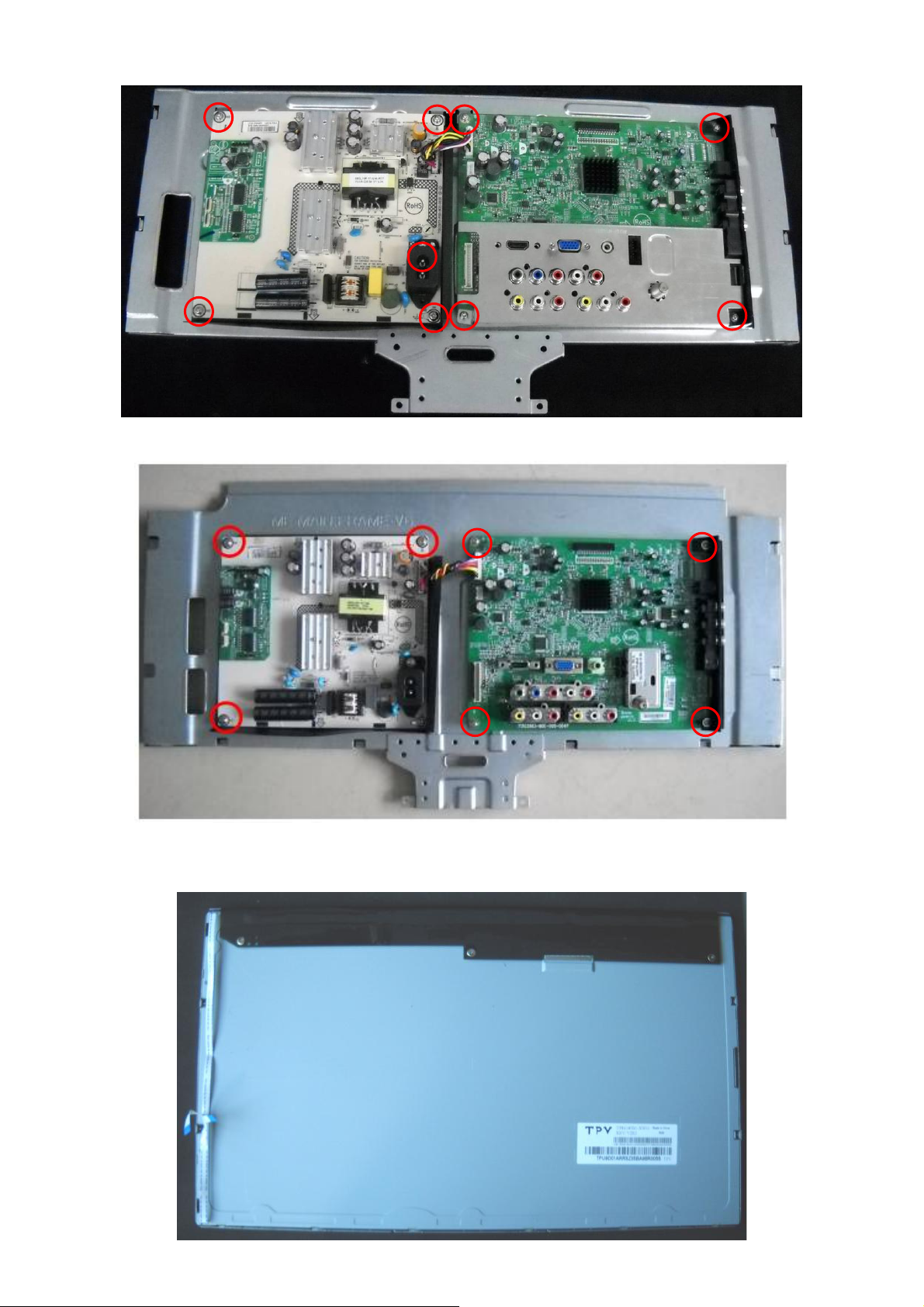
4. Mechanical Instructions
Note: Maybe there are some differences for the below pictures with actual TV, pls base the actual TV, and
below pictures are only for your reference.
1. Unscrew the 4 screws to remove the STAND and BASE.
T942We/ T2442e
T2242We
22
Page 23
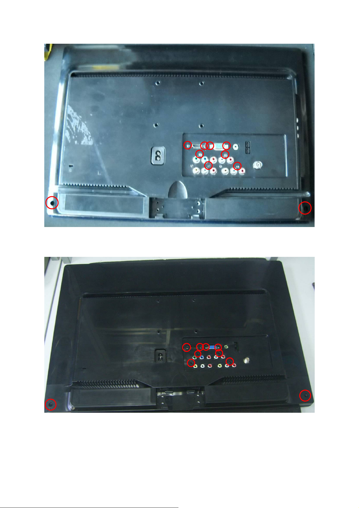
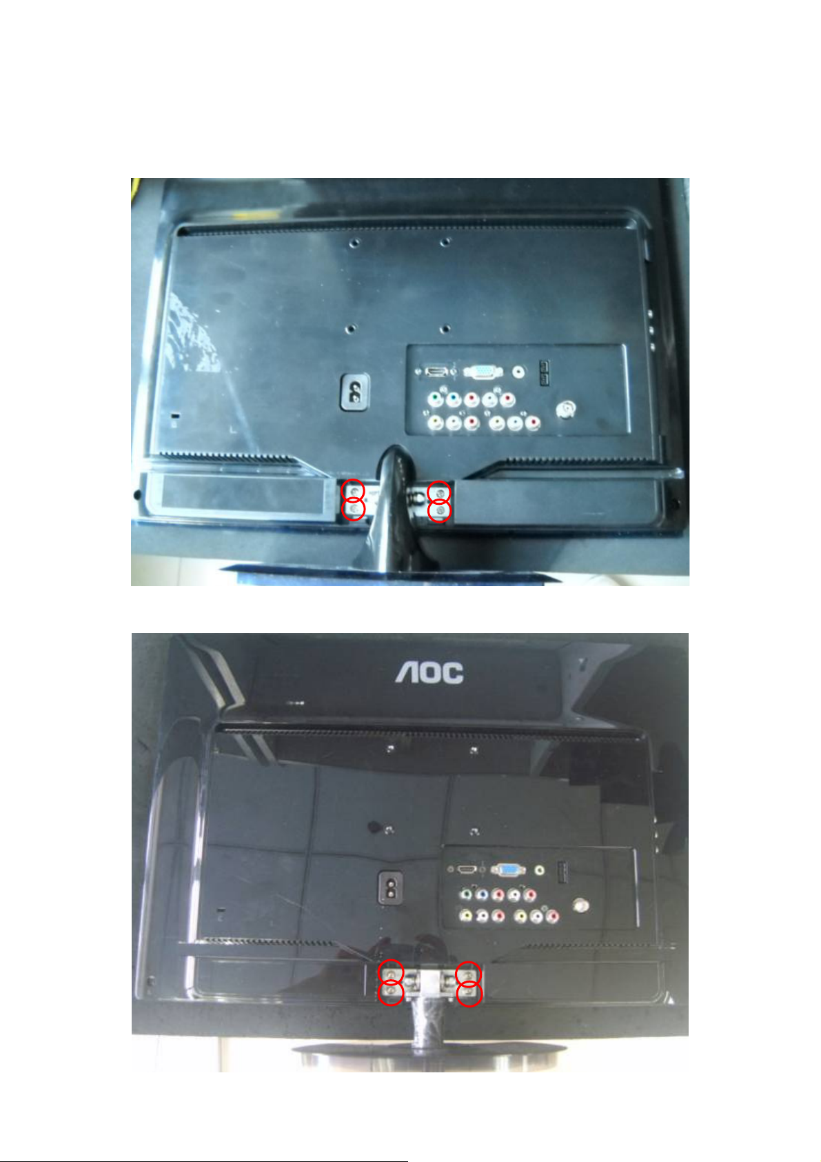
2. Unscrew the 10 screws to remove REAR COVER.
T942We/ T2442e
T2242We
23
Page 24
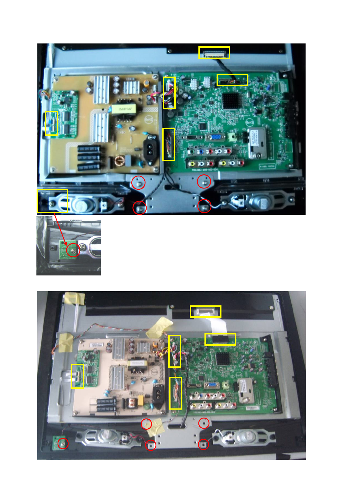
3. Disconnect the connectors , unscrew the 5 screws to remove IR BOARD and separate MAIN FRAME and BEZEL.
T942We
T2242We
24
Page 25

T2442e
4. Unscrew the 2 screws to separate panel and main frame.
5. Unscrew the screws to remove MAIN BOARD and POWER BOARD.
T942We
.
25
Page 26
T2242We
T2442e
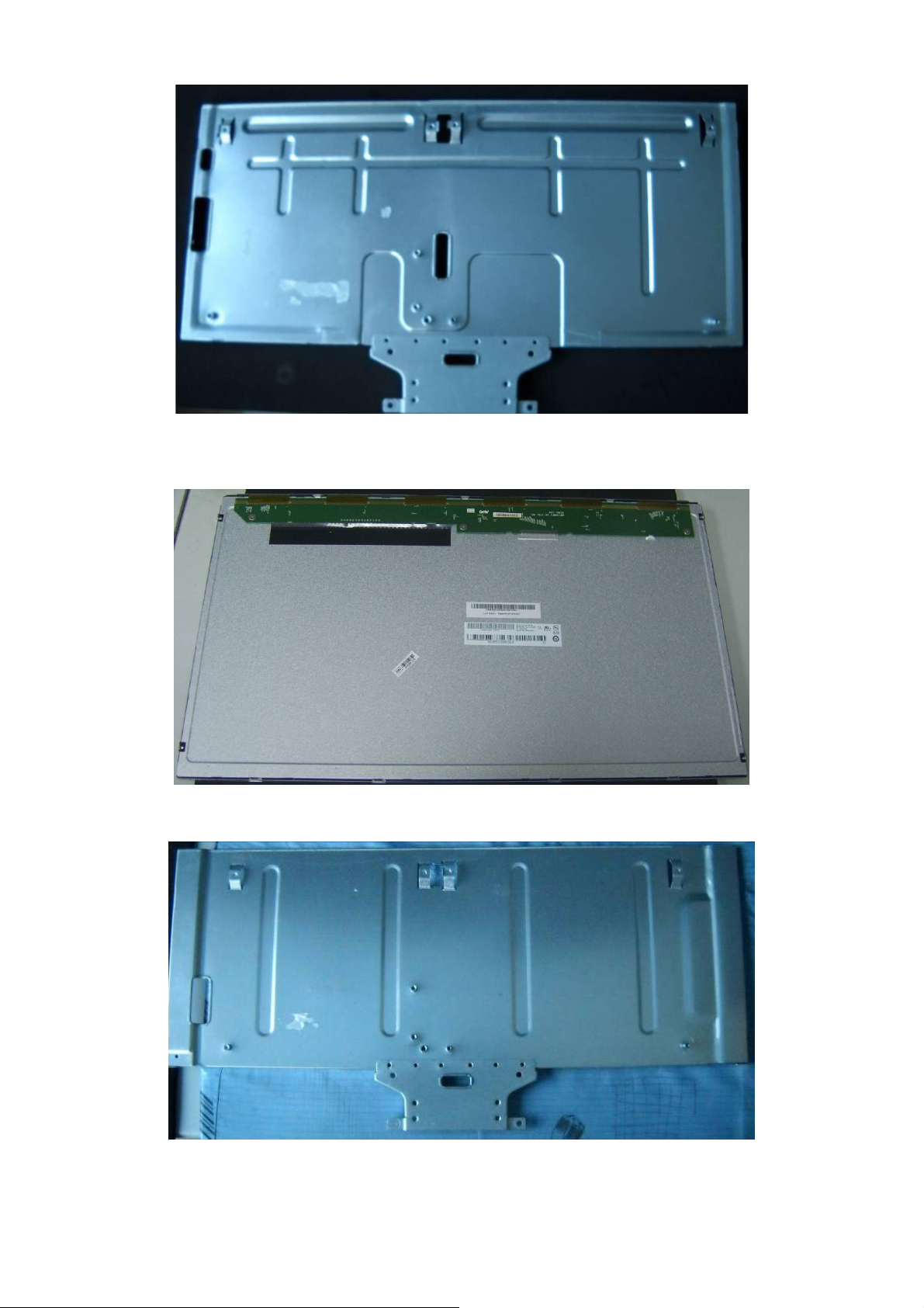
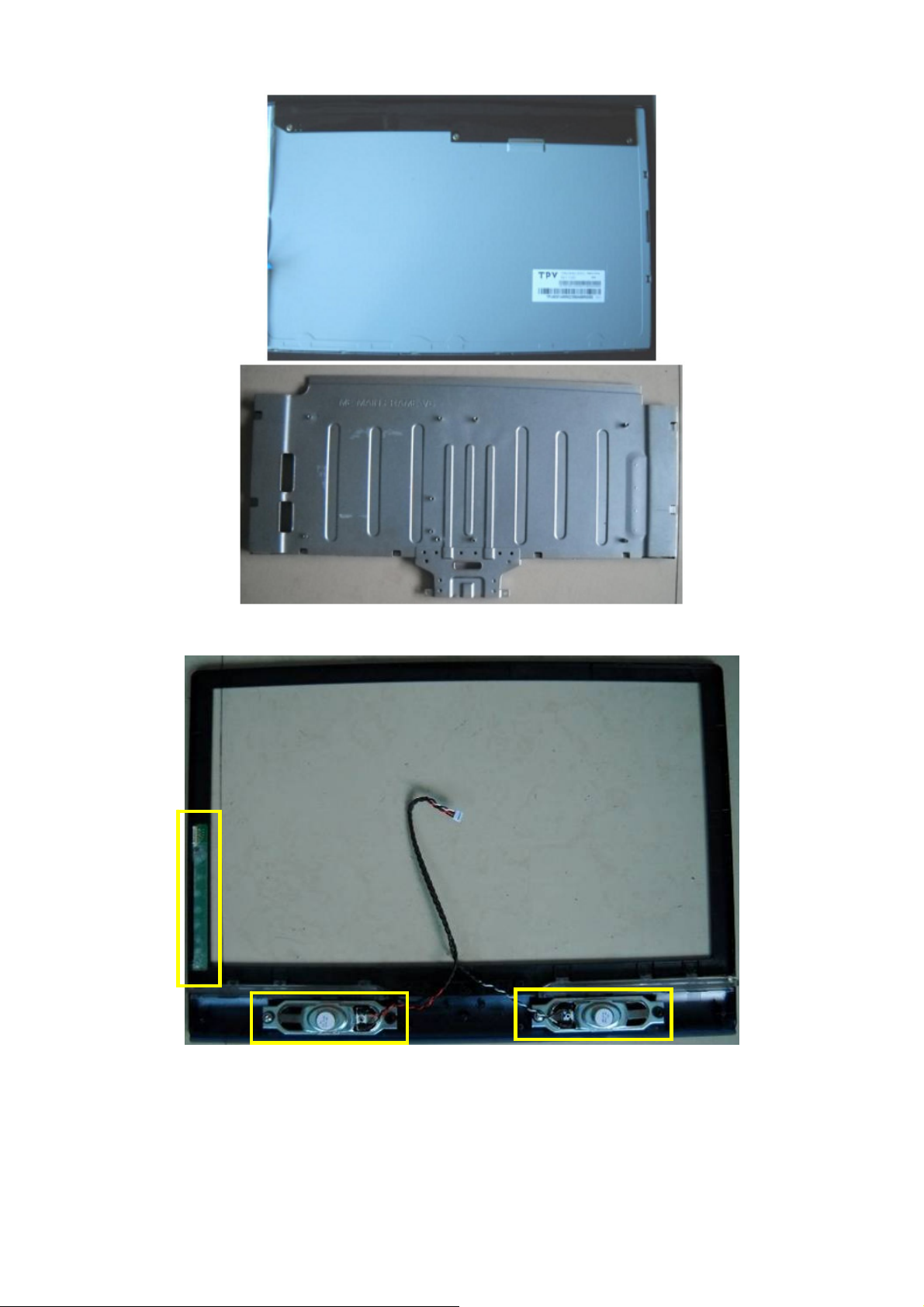
6. The PANEL and MAIN FRAME.
T942We
26
Page 27
T2242We
27
Page 28
T2442e
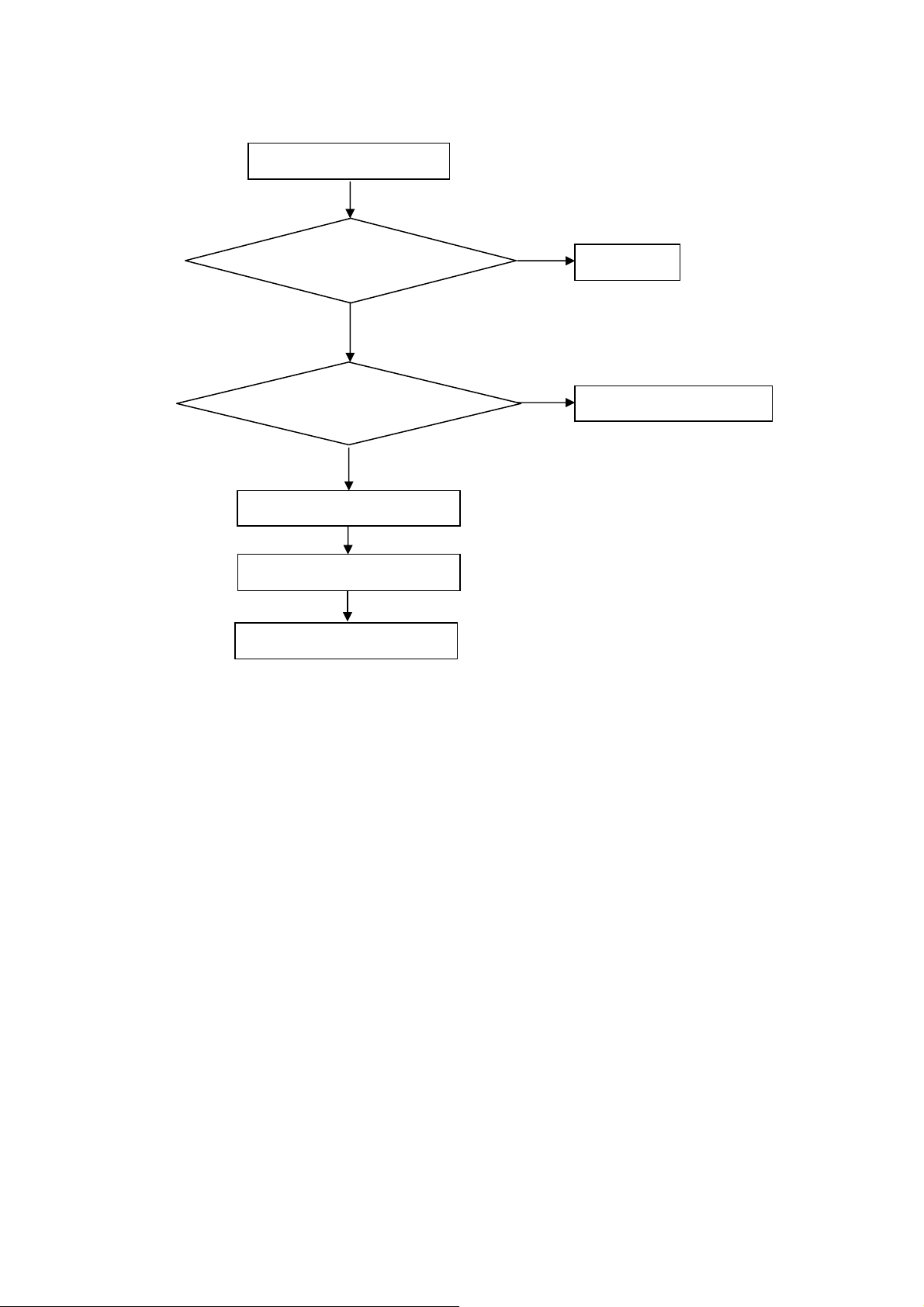
7. Remove the KEY BOARD and SPEAKERS.
28
Page 29
p
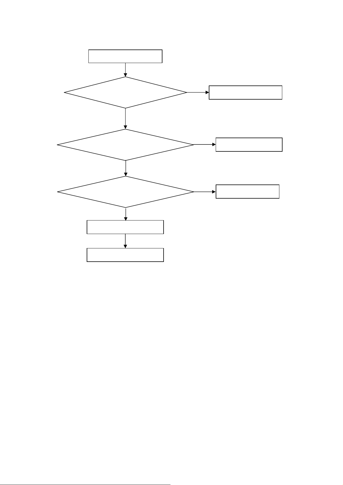
5. Repair Flow Chart
No power
No power (LED “Off”)
Check the AC input and
the
ower is “ON”?
Yes
Power board output=5V?
Yes
Check the IR board and LED
Replace the IR board
No
Replace the main board
No
Power “On”
No
Replace the power board
29
Page 30
Can’t start
Can’t start(LED red)
Power board output=16V?
Yes
Check the power key is under control?
No
Check the IR receiver is normal?
No
Replace the power board
Yes
Replace the key board
Yes
Replace the IR board
No
Replace the main board
No
Replace the Power board
30
Page 31

Abnormal Display
Abnormal Display
Check the source
Yes
Enter factory mode to do
“EEPROM initial”&“Reset”
No
No
Reset the source
Check the main board
Yes
Check the LVDS cable
Yes
Check the panel
No
Replace the panel
No
Replace the main board
No
Replace the LVDS cable
31
Page 32

No display
No display (LED white)
Check TV is under control and power
on/off by remote control and power key?
Yes
Check the LVDS cable
Yes
Yes
Check the backlight is
“On”?
No
Reinsert or replace the
LVDS cable
No
No
Check the B/L
signal is available?
Yes
Replace the main board
No
Replace main board
Panel Vcc = 5V?
Yes
Replace the Panel
No
Replace the main board
Power board output=16V?
Yes
Replace the Panel
Replace the power board
No
32
Page 33

Sound problem
No sound or sound abnormal
Check the audio source connection
and the TV system are correct?
Yes
Check the TV is muted, adjust the
volume or enter the menu to reset?
No
No
Reinsert the audio cable or
change the TV system
Enter factory mode to do “Reset”
No
Check the cable between the
speakers and main board is OK?
Yes
Check the speaker resistance value is in spec
(Remark: The value is marked on the speaker)?
Yes
Replace the cable
Replace the main board
No
No
Replace the speaker
33
Page 34

Remote control malfunction
Remote Control malfunction
Check the remote control battery is
not properly placed or no power?
No
Use the other remote controls
No
Whether the IR board is
abnormal?
No
Replace the main board
Yes
Replace the battery
Yes
Replace the remote control
Yes
Replace the IR board
34
Page 35

OSD is unstable or can’t work normally
OSD is unstable or can’t work normally
Key board connected properly?
Yes
Buttons are OK?
Yes
Key board is OK?
Yes
Enter factory mode to do “Reset”
No
No
No
No
Reconnect the key board
Replace the button function
Replace the key board
Replace the main board
35
Page 36

6. PCB Layout
6.1 Main Board
T942We/T2242we 715G3983M0E000004F
36
Page 37

37
Page 38

T2442e 715G3983M01001004L
38
Page 39

39
Page 40

6.2 Power Board
715G3973P01W21003S
40
Page 41

41 42
Page 42

Page 43

T942we 715G3918P03000004F
43
Page 44

44
Page 45

Converter Board
715G3977P04000004L
45
Page 46

6.3 Key Board
715G4066K01000004S
6.4 IR Board
715G4079R01000004S
46
Page 47

7. Adjustment
It’s no need to adjust the white balance for this model.
1. Enter into the factory mode:
Turn on the TV, press MENU key with remote control, then press number key 1 Æ 9 Æ 9 Æ 9. It will achieve the
factory mode.
2. Click on "Autowhite 100%" in the PC and Component modes:
PC mode: TIM = 107; PAT =48
Component mode: TIM = 311; PAT = 184
Take other model’s factory menu for example:
47
Page 48

8. Block Diagram
CN7602
HDMI
BACK
CN109
YPbPr
CN107
AV&S-VIDEO
SIDE
CN108
BACK
VGA
CN101
AV1
BACK
RX0,RX1,RX2,RXCLK
Y,Pb,Pr
CVBS
Y/C
R,B,G,H,V
RS232
HDMI EDID(U301)
SDA,SCL
CVBS
CVBS
Himax M2D U405
HDMI_RXA0,A1,A2,CLK
AINA2,AINB2,AINC2,SOG2
AINA5
AINB4,AINC4
AINA1,AINB1,AINC1
HSYNC,VSYNC
Himax M2D
AINA3
AINC3,AINB3,AIND1
AIN0_FAD,AIN1_FAD
AIND4
HDMI/ADC
CVBS_O
Himax M2D
TTL/LVDS/RSDS
AV Line Out
(CN110)
LVDS BUS
CN404
LVDS
I/O
BACK
LVDS BUS
PANEL
TU100
BACK
Tuner
IR
ADC KEY
CN103
PC Audio
BACK
AV&S-Video
Audio(CN107)
SIDE BACK
AV1&SCART Option
Audio
(CN104&CN105)
BACK
Tuner
YPbPr
Audio
AV Audio Line Out
BACK
MONO_AUD
COM1_AUL/R
IR_DAT
U601
Switch 4052
SCL,SDA
SIF
SCR_AUOUT_L/R
U404
EEPROM
24C32
MUX_AUL/R
RS232
ADCINN,ADCINP
P0,P1
RAIN0,LAIN0
RAIN2,LAIN2
RAIN1,LAIN1
Himax M2D U405
Himax M2D
MCU
Himax M2D U405
Himax M2D
Audio
48
Himax M2D U405
U402
SPI EEROM
U603
R2A15112FP
U604
APA2176A
Backlight
On/Off,Brightness
CN602
Connector
CN601
Earphone
Page 49

5V_POWER
TPS54286PWPR
U7408
200mA
VCC3
VCC3
MX25L4005AM2C
U402
VCC3AD
VCC3IO / V33LV
HX6201
U405
VCC3AD
VCC3IO
/ V33LV
POWER_ON
AO4449
Q706
1084_33
VCC5
U707
VCC5 AP2176
VCC5
U604
EARPHONE AMP
M24C02
U301
1180mA
VCC18_CORE
281mA
V33_ADC
AP1117D18
U703
AVDD18 / VCCLV
HX6202A
U405
V33ADC / VCCADC / VDDA33
HX6201
U405
39mA
V33_AUD
117mA
VCC18
16mA
VCC18_PLL
M24C02U101
AVDD18 / VCCLV
V33HDMI / VCCADC / VDDA33
V33AUD
HX6201
U405
V18_33HDMI
HX6201
U405
V18AUD / PVDD_LV
V18AUD / PVDD_LV
HX6201
U405
M24C32
U404
V33AUD
16V_POWER
PANEL_ON
Q406
PANEL_VCCAO4449
16V_POWER_AP
R2A15112FP
U603
PANEL
49
Page 50

9. Schematic Diagram
9.1 Main Board
T942We/T2242we 715G3983M0E000004F
CN701
CONN
1
2
3
4
5
6
7
8
9
10
BL_ON1
PWR_ON
V_IPWM
NC
GND
100nF 50V
NC
10K 1/10W
C723
NC
C728
C730
R719
C726
100nF 50V
5VSB
5VSB
GND
5VSB
GND
R728
10K 1/10W
Q710
PMBS3904
GND
R733
NC
Q711
NC
R717
10K 1/10W
Q707
PMBS3904
5V_POWER
GND
V_IPWM
BL_ON1
PWR_ON
1K 1/16W 5%
R734
NC
R720
1K 1/16W 5%
NC
R731
+
C7502
R718
NC
100nF 50V
BL_ADJ 11
16V_POWER
C714
GND
BL_ON 12
PW_ON 12
MCU_5V_POWER _ON13
5VSB
C7545
C7550
10uF 16V
+
C715
NC
100N 16V
R4506
NC
C7552
VCC3
5V_POWER
R4503
NC
NC
Q7503
NC
GND
L7210 47uH
220UF 16V
C7546
C7556
150pF 50V
+
GND
5V_POWER 5VSB
R4501
NC
NC
R4505
GND
20K 1/16W 1%
R4669
6.2K 1/16W 1%
1 2
FB7502 300 OHM
1 2
FB7503 300 OHM
1 2
FB7501 300 OHM
C7501
NC
R4504
Q7502
NC
C7547 33N 50V 1 2
C7548
D7209
1 2
Q7501
B360B
D
D
D
D
8
7
6
5
470UF 25V
GND
GND
+
470pF 50V
C727
R4672
NC
1
S
2
S
3
S
4
G
R4502
NC
NC
U7408
1
PVDD1
2
BOOT1
3
SW1
4
GND
5
EN1
6
EN2
FB17FB2
GND GND
R4673
10OHM1/16W
Vref=0.8V
Vout=Vref*(1+Rup/Rdown)
C7503
100nF 50V
+
GND
Therm al Pa d
PVDD2
BOOT2
SW2
BP
SEQ
ILIM2
TPS54286PWPR
C718
220UF 16V
C7542
10uF 16V
15
14
13
12
11
10
9
8
C701
10UF50V
C7554 33N 50V
C7553
4U7 25V
GND
AZ1117D-1. 8-E1
VCC18
C721
+
100nF 50V
GND
POWER_ON11
VCC5
FB706
300 OHM
1 2
+
GND
U703
ADJ/GN D1OUTPUT2INPUT
GND
C738
100nF 50V
FB7513
120R/6000mA
C7544
470pF 50V
R4670
10OHM1/16W
V33_ADC
3
+
C717
100nF 50V
R729
4.7K 1/10W
U707
G1084-33TU3Uf
VIN3VOUT
GND
1
12
FB709
300 OHM
C716
220UF 16V
2
1 2
5VSB
GND
+
C740
220UF 16V
L7209
22uH
D7208
B360B
10K 1/10W
R725
4.7K 1/10W
R727
4.7K 1/10W
Q709
PMBS3904
V33_ADC
5VSB
R716
GND
2008-11-18
1 2
C739
100nF 50V
R4674
20K 1/16W 1%
R4671
15K 1%
C719
0.1uF 50V
R726
47K +-5% 1/10W
Q708
PMBS3904
2008-9-10
FB701
300 OHM
C734
+
220UF 16V
C7543
100P 50V
220UF 16V
AO4411
1
2
3
4
R721
100K 1/10W
V33_AUD
C735
100nF 50V
VCC18_CORE
C7555
+
C7551
100N 16V
GND
VCC5
Q706
8
S
D
7
S
D
6
S
D
5
G
D
VCC3
+
100UF16V
GND
C722
C748
1nF 50V
C733
100nF 50V
C749
1nF 50V
1nF 50V
50
GND GND
T P V ( Top Victory Electronics Co . , Ltd. )
絬 隔 瓜 絪 腹
Key Component
03.Power
Date
OEM MODEL
TPV MODEL
PCB NA ME
Sheet
715G3806-M0A-000-0040
412Tuesday , June 01, 2010
of
GND
GND
A3
Size
Rev
A
<
称爹
称爹
>
Page 51

VCC3_HD
20
21
22
23
24
20
22
23
21
ZD7506
ZD7508
ZD7509
ZD7507
ZD7505
ZD7504
CN7601
NC
TH1
TH2
TH3
TH4
TH5
TH1
TH3
TH4
TH2
12
12
12
CE Remote
DDC DATA
12
12
12
CE Remote
DDC DATA
DDC_WP
DDCB_SCL-
DDCB_SDA-
CN7602
HDMI
D2+
D2 Shield
D2-
D1+
D1 Shield
D1-
D0+
D0 Shield
D0-
CK+
CK Shield
CK-
NC
DDC CLK
GND
+5V
HP DET
DDC_WP
DDCA_SCL-
DDCA_SDA-
RClamp0520B.TCT
D2+
D2 Shield
D2-
D1+
D1 Shield
D1-
D0+
D0 Shield
D0-
CK+
CK Shield
CK-
NC
DDC CLK
GND
+5V
HP DET
1
2
3
4
5
6
7
8
9
10
11
12
13
14
15
16
17
18
19
ZD7503
1
2
3
4
5
6
7
8
9
10
11
12
13
14
15
16
17
18
19
124
124
DDCA_SCL
DDCA_SDA
HDMIA_5VIN
HDMIA_HPD
2
RXB2P_M2-
RXB2N_M2-RXB1P_M2-
RXB1N_M2RXB0P_M2-
RXB0N_M2RXBCLKP_M2-
RXBCLKN_M2HDMIB_CEC-
DDCB_SCL
DDCB_SDA
HDMIB_5VIN
HDMIB_HPD
L7211
90 ohm
L7213
90 ohm
3
3
L7212
124
3
90 ohm
L7214
124
90 ohm
R4555 0R05 1/10W
R4556 0R05 1/10W
R4509 1K 1/16W 5%
5V_POWER 5V_POWER
R4665
0R05 1/16W
Q7504
NC
R4512
1
0R05 1/10W
L7201
124
NC
L7203
124
NC
R4515 NC
R4518 NC
R4511
NC
HDMIB_HPD
Q7507
NC
HDMIA_HPD
Q7520
BC847C
3
3
1 2
FB7504
R4513
3
3
1 2
FB7505
NC
R4536
NC
R4535
4.7K1/16W
RXA2P_M2-
RXA2N_M2RXA1P_M2-
RXA1N_M2RXA0P_M2-
RXA0N_M2RXACLKP_M2-
RXACLKN_M2-
BEAD
R4666
NC
Q7505
2N7002
0R(NC)
NC
ZD7502
HDMI_LP/12
HDMI_DET_A
4.7K1/16W
DDCA_SCLDDCA_SDA-
ZD7501
1 3
BZX84-C5V6
L7202
124
NC
L7204
124
NC
C7517
NC
1 3
HDMI_DET_B
DDCB_SDADDCB_SCLRXBCLKN_M2H
RXBCLKP_M2H
RXB0N_M2H
RXB0P_M2H
RXB1N_M2H
RXB1P_M2H
RXB2N_M2H
RXB2P_M2H
R4510
DDC_WP
C7516
100N 16V
3
3
HD5V_A
VCC5_HD
Q7506
NC/BC847C
R4525
4.7K1/16W
VCC3
R4533
0R05 1/16W
VCC5
R4663
0R05 1/16W
R4554
27K 1/16W
RXB2P_M2H
RXB2N_M2H
RXB1P_M2H
RXB1N_M2H
RXB0P_M2H
RXB0N_M2H
RXBCLKP_M2H
RXBCLKN_M2H
HD5V_B
R4534
0R05 1/16W
49
NC
50
HPD2
51
SDA2
52
SCL2
53
B21
54
A21
55
VCC
56
B22
57
A22
58
GND
59
B23
60
A23
61
VCC
62
B24
63
A24
64
NC
132
R4527
10K1/16W
3V3_EX_MCU
R4664
NC
RXA2P_M2-
48
R4538 1K 1/16W 5%
HD5V_A
D7201
BAT54C
R4544 100R 1/ 16W 5%(NC)
C7513
220N 10V
U7401
8
A0
VCC
7
A1
WP
6
A2
SCL
5
GND
SDA
M24C02-WMN6TP
HA_CEC 13
DDCA_SCL-
RXACLKN_M2-
RXA1P_M2-
RXA0P_M2-
DDCA_SDA-
HDMI_DET_A
RXACLKP_M2-
RXA2N_M2-
RXA0N_M2-
RXA1N_M2-
35
36
37
43
40
46
39
42
45
B1138A11
B1241A12
B1344A13
B1447A14
VCC
VCC
GND
SCL1
SDA1
HPD1
HPD_SINK
SDA_SINK
SCL_SINK
NC1NC2GND3NC4NC5VCC6NC7NC8GND9NC10NC11VCC12NC13NC14GND15VSADJ
R4539 1K 1/16W 5%
R4540 1K 1/16W 5%
R4541 1K 1/16W 5%
R4542 1K 1/16W 5%
R4543 1K 1/16W 5%
R4546 1K 1/16W 5%
R4547 1K 1/16W 5%
R4548 1K 1/16W 5%
R4549 1K 1/16W 5%
1
2
3
4
34
33
S2
EQ
GND
VCC
GND
VCC
16
R4516
0R05 1/10W
U7403
AZHW251R
32
S1
31
30
29
28
27
Z1
26
Y1
25
24
Z2
23
Y2
22
21
Z3
20
Y3
19
18
Z4
17
Y4
R4537
6K2 1/10W 1%
R4521
NC
DDC_WP
DDCB_SCLDDCB_SDA-
VCC3_HD
DDC_WP_EN12
NC
L7205
124
90 ohm
L7207
124
90 ohm
R4528
10K1/16W
R4522
R4560
VCC5
1K 1/16W 5%
3
3
10K 1/10W
1K 1/10W
VCC3_HD
R4526
10K1/16W
132
R4523
NC
R4558
123Q7511
PMBS3906
HDMI_S2/SDA 12
HDMI_S1/SCL 12
D7206
NC
R4545 NC
C7518
NC
8
VCC
7
WP
6
SCL
5
SDA
NC
VCC5_HD
R4531
C7519
NC
L7206
124
90 ohm
L7208
124
90 ohm
R4557
HD5V_B
U7402
GND
R4507
2K OHM
100 OHM 1/10W
1
A0
2
A1
3
A2
4
R4508
2K OHM
C7520
NC
R4514 20R 5% 1/16W
R4517 20R 5% 1/16W
R4519 20R 5% 1/ 16W
R4520 20R 5% 1/ 16W
3
R4524 20R 5% 1/ 16W
R4529 20R 5% 1/ 16W
R4530 20R 5% 1/ 16W
R4532 20R 5% 1/ 16W
3
Q7510
PMBS3904
HPDA 9
DDCHA_SDA 9
DDCHA_SCL 9
DDC_WP 7
VCC3
RXACLKN_M2 9
RXACLKP_M2 9
RXA0N_M2 9
RXA0P_M2 9
RXA1N_M2 9
RXA1P_M2 9
RXA2N_M2 9
RXA2P_M2 9
HDMIA_5VIN
HDMIB_5VIN
1 2
FB7506
R4552
10K 1/10W
R4553
NC
BEAD
HD5V_A
VCC5
5VSB
5VSB
C7504
10uF 16V
132
132
R4550
10K 1/10W
Q7508
PMBS3904
R4551
NC
Q7509
NC
D7203
HA5V_DET
HB5V_DET
C7505
100N 16V
BAT54C
D7204
BAT54C
HA5V_DET 12
HB5V_DET 12
C7506
C7507
100N 16V
100N 16V
HD5V_B
C7514
100N 16V
C7508
100N 16V
C7515
100N 16V
C7509
100N 16V
VCC5_HD
C7510
100N 16V
C7511
100N 16V
C7512
100N 16V
VCC3_HD
51
T P V ( Top Victory Electronics Co . , Ltd. )
絬 隔 瓜 絪 腹
Key Component
04.HDMI
Date
OEM MOD EL
TPV MOD EL
PCB NAME
Sheet
715G3806-M0A-000-0040
512Tuesday, June 01, 2010
of
A2
Size
Rev
A
<
称爹
>
称爹
Page 52

1
ANT IN
NC
NC
2
TGND
R320
100 OHM 1/10W
AS
3
TU1 00
SDA4SCL5SIF
SCL
SDA
6
7
R317
100 OHM 1/10W
5V for Tuner
8
G965-25ADJ PIUF
2.2 OHM 1/10W
C219
100UF16V
R208
U159
R739
C206
0.1uF 50V
GND
VEN1VIN2VO3ADJ
36KOHM +-1% 1/8W
GND5GND6GND7GND
4
R4689 0R051/ 8W
+
C218
100UF16V
R172
12K1/10W
R173
T_CVBS 9
Put Near
to IC
+5VT
VCC5
12
TH1
13
TH2
14
TH3
15
TH4
Vcc
NC
AGC
9
8
T5V
VIDEO OU T
AUDI O OUT
11
10
TGN D
+5VT
2008/11/05
FB300
R207
0R05 1/16W
C208
220pF 50V
TV_CVBS
100UF16V
SIF 10
SCL_A_Tuner 12
SDA_A_Tuner 12
C308
TGN D
+
C309
100nF 50V
remove
C207
R206
2.2uH
R212
0R05 1/16W
TV_CVBS T_CVBS
220pF 50V
TGN D
+
100 OHM 1/10W
R210
75OHM1/16W
C324
56pF 50V
TGND
C323
56pF 50V
52
T P V ( Top Victory Electronics Co . , Ltd. )
絬 隔 瓜 絪 腹
Key Component
05.TUNER
Date
OEM MOD EL
TPV MOD EL
PCB NAME
Sheet
715G3806-M0A-000-0040
of
612Tuesday , June 01, 2010
Size
Rev
称爹
A3
A
称爹
>
<
Page 53

CN109
E
D
C
B
A
JACK
R151
100OHM1/16W
RX
VGASDA_IN
VGA_HIN
VGA_VIN
VGA_HIN
CN103
PHONEJAC K
PHONEJAC K
11
10
9
8
7
6
5
4
3
2
1
VGASCL_IN
AZC199-04S
2
1
U101
3
2
1
COM_AUR
COM_AUL
COM_AUL
COM_AUR
UART_RX 11
11
12
13
14
15
I/O23I/O3
GND
VDD
I/O1
I/O4
VGA_AUR_O
VGA_AUL_O
PR
PB
Y
CN108
1716
1
6
2
7
3
8
4
9
5
10
18 19
CONN
4
5
5VSB
6
Y
VPORT0603100KV05
VPORT0603100KV05
PB
VPORT0603100KV05
VPORT0603100KV05
PR
VPORT0603100KV05
VPORT0603100KV05
RED
RED_GND
GRN
GRN_GND
BLU
BLU_GND
100OHM1/16W
ZD114
1 2
VPORT0603100KV05
VGA PIN DEFIINITION
1 R_OUT
2 G_OUT
3 B_OUT
4 NC
5 GND
C113 4U7 25V
R116
27K 1/10W
C114 4U7 25V
R115
27K 1/10W
R122
R121
100K 1/10W 5%
100K 1/10W 5%
ZD107
1 2
ZD108
1 2
ZD109
1 2
R211
27K 1/10W
R205
27K 1/10W
R215
R209
100K 1/10W 5%
100K 1/10W 5%
R148
6 R_GND
7 G_GND
8 B_GND
9 +5V(DDC)
10 GND
UART_TX 11
11 NC
12 DDC SD A
13 TTL H-S
14 TTL V-S
15 DDC SC L
VGA_AUR 10
VGA_AUL 10
R656
75 OHM 1/10W
R657
75OHM1/16W
R655
75OHM1/16W
C179
4U7 25V
C182
4U7 25V
VGA_5V_A
0R05 1/10W
C171
0R05 1/10W
NC
0R05 1/10W
0R05 1/10W
C172
NC
0R05 1/10W
0R05 1/10W
C173
NC
U103
AZC199-04S
BLU
DDC_WP5
R168
R167
R166
COM1_AUL 10
COM1_AUR 10
RED
1
I/O1
6
5VSB
VGASDA_IN
VGASCL_IN
C175
NC
C174
NC
C170
NC
RX
2
3
I/O2
GND
I/O34VDD5I/O4
GRN
R4561
4.7K1/16W
VGA_DDCSCL
VGA_DDCSDA
R203 0R05 1/16W
R169 0R05 1/16W
Near to IC
4.7K1/16W
R246
100OHM1/16W
100OHM1/16W
R222
100OHM1/16W
100OHM1/16W
R224
100OHM1/16W
100OHM1/16W
R245
100OHM1/16W
100OHM1/16W
VCC5
R4562
VGA_DDCSD A 9, 13
VGA_DDCSC L 9,13
C184
C183 1N 50V
C186
C185
1
R4563
10K1/16W
47N 50V
47N 50V
47N 50V
D7202
2
3
BAT54C
R4564100R 1/ 16W 5%(NC)
C7521
220N 10V
8
VCC
7
WP
6
SCL
5
SDA
M24C02-WMN6TP
Y1 9
SOY1 9
GND
PB1 9
GND
PR1 9
GND
VGA_5V_A
U7404
A0
A1
A2
GND
GRN
GRN_GND
RED
1
2
3
4
RED_GND
BLU
BLU_GND
T P V ( Top Victory Electronics Co . , Ltd. )
絬 隔 瓜 絪 腹
Key Component
06.VGA/Y PbPr Connector
Date
R161
75 OHM 1/10W
R149
75 OHM 1/10W
R150
75 OHM 1/10W
VGA_VIN
VGA_HIN
1 2FB7514 60 OHM
C147
NC 180pF 50V
1 2FB7515 60 OHM
C117
NC 180pF 50V
1 2FB7516 60 OHM
C142
NC 180pF 50V
C146
NC 180pF 50V
C141
NC 180pF 50V
C143
NC180pF 50V
2.2K 1/10W
R127
120 OHM
FB103
2.2K 1/10W
OEM MOD EL
TPV MOD EL
PCB NAME
Sheet
R144
UART_TX11
UART_RX11
715G3806-M0A-000-0040
712Tuesday, July 20, 2010
R156
100OHM1/16W
R164
100OHM1/16W
R157
100OHM1/16W
R155
100OHM1/16W
Near to IC
C148
22P 50V
C150
22P 50V
of
100OHM1/16W
R126
100OHM1/16W
VCC3
C155 1N 50V
C152
47N 50V
C154
47N 50V
47N 50V
R125
(TX)
(RX)
VCC1
C153
1
2
3
CN7603
CONN
SOGAIN 9
GAIN 9
RAIN 9
BAIN 9
VSYNC 9,13
HSYNC 9,13
Size
Rev
称爹
A3
A
<
称爹
>
53
Page 54

CVBS1_IN
ZD101
CVBS_GND
SY_I N
SY_GN D
SC_IN
SC_GND
VPORT0603100KV05
ZD102
VPORT0603100KV05
ZD103
VPORT0603100KV05
S-video
SC_GND
CVBS & R/L
CN107B
JACK
2
1
4
3
6
5
CN107A
JACK
12
7 8
CY
9 10
GG
CVBS1_IN
CVBS_GND
R252
27K 1/10W
R256
27K 1/10W
R259
R253
100K 1/10W 5%
100K 1/10W 5%
SY_I NSC_IN
SY_GN D
11
C192
4U7 25V
C193
4U7 25V
SV/AV_AUL 10
SV/AV_AUR 10
VCC5
L101
2.2uH
1 2
L102
2.2uH
1 2
L103
2.2uH
1 2
C189
220P 50V
C190
220P 50V
C187
220P 50V
CVBS2_IN
CVBS_GND
L105
L106
2.2uH
2.2uH
ZD104
1 2
VPORT0603100KV05
C217
220P 50V
C216
220P 50V
0R05 1/16W
L111
2.2uH
R254
0R05 1/16W
R257
0R05 1/16W
R250
Near to IC
L104
C214
220P 50V
2.2uH
R247
100OHM1/16W
R248
75OHM1/16W
R255
100OHM1/16W
R249
75OHM1/16W
R251
100OHM1/16W
R258
75OHM1/16W
R267
0R05 1/16W
C197
220P 50V
100N 16V
100N 16V
100N 16V
R260
100OHM1/16W
R261
75OHM1/16W
C194
C188
C191
CVBS 9
GND
SV_Y 9
GND
SV_C 9
GND
C202
100N 16V
SCR_Y 9
GND
AV-OUT
CN110
A
B
C
JACK
2
1
4
3
6
5
GND
C195
100N 16V
FB107
1 2
121 OHM
220pF 50V
C196
100P 50V
C211
CVBS signal output
GND
23
R263
75OHM1/16W
C198
470pF 50V
Q110
1
PMBS3906
R273
150 OHM 1/10W
R278
120OHM 1/10W
FB105
600 OHM
R280
200 OHM 1/10W
Q111
PMBS3904
GND
FB106
600 OHM
C209
470pF 50V
R277
47K +-5% 1/10W
C210
10uF 16V
R262
47K +- 5% 1/10W
GND
C205
4U7 25V
C200
4U7 25V
R271
100K 1/10W 5%
100K 1/10W 5%
CVBS_O
GND
R274
C782
NC
GND
CVBS_O 9
R279
680R 1/16W 5%
R264
680R 1/16W 5%
C204
4U7 25V
C203
4U7 25V
54
SCR_AU OUT_L 10
SCR_AU OUT_R 10
T P V ( Top Victory Electronics Co . , Ltd. )
絬 隔 瓜 絪 腹
Key Component
Date
07.SCAR T SV/AV
JACK
CN101
CVBS2_IN
2
A
CVBS_GND
1
4
B
3
6
C
5
OEM MO DEL
TPV MODEL
PCB NAME
Sheet
R265
27K 1/10W
R270
27K 1/10W
R272
R266
100K 1/10W 5%
100K 1/10W 5%
715G3806-M0A-000-0040
812Tuesday , June 01, 2010
C199
4U7 25V
SCR_AU _L 10
C201
4U7 25V
SCR_AU _R 10
Size
Rev
of
称爹
A3
A
<
称爹
>
Page 55

V33_ADC
1 2
C305
10uF 16V
VCC18
1 2
FB306 300 OHM
VCC18
VCC3
V33_ADC
FB303
1 2
300 OHM
C316
10uF 16V
FB307
1 2
300 OHM
1 2
C325
10uF 16V
FB302
300 OHM
HDMI 3.3V POWER
C306
100nF 50V
GNDGND
C312
100nF 50V
GND
AVDD18
C317
100nF 50V
GNDGND
V33ADC_PLL
C328
C330
100nF 50V
100P 50V
ADC 3.3V POWER
FB301 300 OHM
V33ADCV33ADC
V33HDMI
C307
100nF 50V
V18_33HDMI
C313
100nF 50V
C318
100nF 50V
C329
100nF 50V
GND
C326
100nF 50V
C314
100nF 50V
V33ADC
V33ADC1
V33ADC1
AVDD18
V18_33HD MI
V33HDMI
176
1
175
5
U405A
GND
3
HDMI_RXACKN
4
HDMI_RXACKP
6
HDMI_RXA0N
7
HDMI_RXA0P
8
HDMI_RXA1N
9
HDMI_RXA1P
10
HDMI_RXA2N
11
HDMI_RXA2P
170
GPIO_52/HPD
171
GPIO_53/CEC
172
GPIO_54/HDMIDDC_SDA
173
GPIO_55/HDMIDDC_SCL
13
EXT_R
168
GPIO_47/DSUBDDC_SDA/UART_TX1
169
GPIO_48/DSUBDDC_SCL/UART_RX1
2
VSSD(0V)
17
VSSDP_AD (0V)
42
VSSA_AD(0V)
174
VSSD_AL(0V)
177
GND
HX6201
RXACLKN_M25
RXACLKP_M25
RXA0N_M25
RXA0P_M25
RXA1N_M25
RXA1P_M25
RXA2N_M25
RXA2P_M25
HPDA5
HA_CEC _M2D+13
DDCHA_SDA5
DDCHA_SCL5
VGA_DDCSDA7,13
VGA_DDCSCL7,13
V33HDMI REXT
R315
0R05 1/16W
R318 390 OHM 1/10W
R301
R319
0R05 1/16W
0R05 1/16W
12
DVCC(1.8V)
AVDD33_RX
VDD18(1.8V)
VDDA_AL(1.8V)
VDDD _AL(1.8V)
HDMI/ADC
V33ADC _PLL
36
22
19
45
14
FILT
HSYNC
VSYN C
AINA1
AINB1
SOG1
VDDA_AD(3.3V)41VDDA_AD(3.3V)
VDDP_AD(3.3V)
VDDD_AD(3.3V)
BVDDA_AD(3. 3V)
VDDD P_AD(3.3V)
AINC 1
AINA2
SOG2
AINB2
AINC 2
AINA3
SOG3
AINB3
AINC 3
AIND 1
AINA5
AINB4
AINC 4
AIND 4
AOUT1
AOUT2
AIN0_FAD
AIN1_FAD
AIN2_FAD
VMIDS
VREF
18
15
16
23
24
25
26
27
28
29
30
31
32
33
34
35
37
38
39
40
43
44
48
47
46
VMID
20
ADC_VREF
21
100nF 50V
FILT
C315 100nF 50V
C319 100nF 50V
C333 100nF 50V
C335 100nF 50V
C321
GND GND
C301
10N 50V
R314
1K62 1/10W 1%
C322
10uF 16V
V33ADC _PLL
V33ADC _PLL
C311
100nF 50V
HSYNC 7,13
VSYN C 7, 13
BAIN 7
GAIN 7
SOGAIN 7
RAIN 7
SCR_Y 8
SOY1 7
Y1 7
PB1 7
PR1 7
T_C VBS 6
SV_C 8
SV_Y 8
CVBS 8
CVBS_O 8
GND
GND
C7540 100nF 50V
C7539 100nF 50V
C320 100nF 50V
GND
1 2
FB305
300 OHM
V33ADC1
C327
C331
100nF 50V
100nF 50V
GNDGND
C332
100nF 50V
GND
T P V ( Top Victory Electronics Co . , Ltd. )
絬 隔 瓜 絪 腹
Key Component
08.M2D HDMI/Analog I/O
Date
55
OEM MODEL
TPV MO DE L
PCB NAME
Sheet
715G3806-M0A-000-0040
of
912Tuesday , June 01, 2010
Size
Rev
称爹
A3
A
称爹
>
<
Page 56

VCC3
V33_AUD
SIF6
0R05 1/16W
VGA_AUR7
VGA_AUL7
SCR_AU_R8
SCR_AU_L8
SV/AV_AUR8
SV/AV_AUL8
COM1_AUR7
COM1_AUL7
AGSCRT
FB606
1 2
GND
R602
VREF_AD C
VCM_ADC
VBG
VRN
VRP
C625
10uf 6. 3V
300 OHM
FB602
1 2
C604
10uF 16V
R604
NC
GND GN D
SIF1SIF1+
C631
C629
C627
100nF 50V
10UF 6.3V
100nF 50V
GND
VCC3AD
C663
100nF 50V
GND
300 OHM
GND
C602
0.1uF 50V
SIF1+
SIF1-
C603
0.1uF 50V
77
78
49
50
52
53
54
55
56
57
59
60
61
62
63
64
V33AUD
C605
100nF 50V
U405B
ADCINN
ADCINP
RAIN0
LAIN0
RAIN1
LAIN1
RAIN2
LAIN2
RAIN3
LAIN3
VREF_ADC
VCM
AGSCRT
VBG
VRN
VRP
HX6201
C661
100nF 50V
VCC3AD
79
65
AVDD_DAC(3.3V)
AVDD(3.3V)(ForPIFADC)
AUDIO
C606
100nF 50V
V33AUD
58
VDDA(3.3V)
GPIO_03/PIF_AGC
GPIO_04/PIF_AMP
GPIO_02/SPDIFI
GPIO_40/SP DIFO
DAC_LSR
DAC_LSL
SCART1R
SCART1L
SCART2R
SCART2L
VREF(ForPIFADC )
SIF_VCMG
SIF_VRE FN
SIF_VREFP
VSSA(0V)
SIF_VRE FP
SIF_VREFN
16V_POWER
1 2
1 2
C617
100nF 50V
C634
100nF 50V
FB422
300 OHM
FB7511
300 OHM
VCC5
C648
C649
12
11
10
9
GND
GND
GND
R614
5.6KOHM + -1% 1/10W
R615 33K 1/10W
PGND
R618
5.6KOHM + -1% 1/10W
PGND
SGND
SPK_ROUT
SPK_LOUT
C659
100nF 50V
FB7521
FB7522
FB7523
1U 25V
PGND
Q603
PMBS3904
100nF 50V
C650 1uF 25V
C655 1uF 25V
GND
0.05R
0.05R
0.05R
C643
C644 10uF 16V
C646
10uF 16V
SGND
C651 10uF 16V
GND
CN601
5
4
3
2
6
7
1
PHONEJACK
To SPK_L
10uF 16V
AMP5VO
C652
1U 25V
C654
1U 25V
SGND
270K 1/10W 5%
10uF 16V
U604
15
13
SGND
2 3
C645
1uF 25V
NC
VCC5
+
C660
R616
10K1/16W
Q601
PMBS3904
SGND
PGND
PGND
R639
10K 1/10W
Q413
PMBS3906
C672
100UF16V
16
PVDD
1
CP+
2
APA2176A
PGND
3
CP-
4
NC
CVSS5VSS6LOUT7VDD
VCC5
R634
5.1K 1/10W
GND
STBY:
L: 10uA
STBY
C639
0.1uF 50V
SGND
R4684 0R05 1/16W
C7561
NC
R4683 0R05 1/16W
C7560
NC
VCC5
47K 1/16W 5%
FOR AC "PO PO"
10/31/08
NC
GND14/LSD
RIN
/RSD
LIN
ROUT
8
C658
100nF 50V
R620
5VSB
R603
SW_AMP_RIN
SW_AMP_LIN
GND
GND
VREFI_PIF
SIF_VCMG
SIF_VRE FN
SIF_VRE FP
C620
100nF 50V
SW_AMP_LIN
SW_AMP_RIN
NC
SCR_AUOUT_R 8
SCR_AUOUT_L 8
C611
100nF 50V
VRN
VRP
C621
100nF 50V
STYAMP_MUT12
R4680 12K 1/16W 1%
R4682 12K 1/16W 1%
AMP_MUT12
84
85
86
167
70
71
68
69
66
67
73
74
75
76
51
EAR_DET
SW_AMP_RIN 11
SW_AMP_LIN 11
C613
100nF 50V
GND
C622
10uF 16V
C623
100nF 50V
GND
10K 1/10W
PGND
PGND
R622
10K 1/10W
5VSB
GND
C647
1uF 25V
VCC3
C7557
0.1uF 50V
GND
EAR_DET
R613
R4685 1KOHM +- 1% 1/16W
C7558
1N 50V
R4681 1KOHM +- 1% 1/16W
C7559
1N 50V
R638
1
10K 1/10W
R637
10K 1/10W
SGND
SGND
R642
R643
SGND
13
14
15
16
17
18
19
20
21
22
23
24
C662
NC
0R05 1/16W
0R05 1/16W
C664
NC
16V_POWER_AP
C635
0.1uF 50V
R619
0R05 1/10W
49
TGND
CBIAS
ROSC
AVCC
GND
NC
NC
NC
NC
NC
CLOCK
VREF
PROT
R617
NC
R799
GND
2008-11-07
C615
1.5nF 50V
1K 1/16W 5%
R612
1K 1/16W 5%
R611
C616
1.5nF 50V
10K 1/10W
GND
+
C636
470UF 25V
SGND
SGND
11
5
12
9
10
NC6NC7NC8NC
IN1
GAIN1
STBYL
IN225GAIN226MUTEL27NC28NC29NC30NC31VD232VD233NC34OUT235OUT2
SGND
C667
0.1uF 50V
SGND
VD14VD1
GND
SGND
3
2
NC
SGND
SW_AMP_RIN
SW_AMP_LIN
R633
OUT11OUT1
NC
VS1
VS1
NC
HB1
NC
DVDD
HB2
NC
VS2
VS2
NC
36
C657
0.1uF 50V
PW_GND
C638
0.1uF 50V
U603
R2A15112FP
48
47
46
45
44
43
42
41
40
39
38
37
C665
0.1uF 50V
16V_POWER_AP
GND
C653
Q604
PMBS3904
MUTE_H PHO NE 1 2
L600
22uH +-25%
C641
0.1uF 50V
10uF 16V
L601
22uH +-25%
VCC5
R630
47K 1/16W 5%
GND
SGND
SGND
C656
NC
GND
FB7517 300 OHM
C640
470UF 25V
+
1 2
C642
330N 50V
C668
330N 50V
1 2
+
C666
470UF 25V
PGND
SGND
絬 隔 瓜 絪 腹
Key Component
16V_POWER
2 3
R4565
SGND
R4567
CN602
4
3
2
1
CONN
1
D7205
BAS316
123Q7513
R4566
47K 1/16W 5%
2N3906S-RTK/PS
1K 1/16W 5%
47K 1/16W 5%
SGND
FB7518
300 OHM
T P V ( Top Victory Electronics Co . , Ltd. )
09.M2D Audio
Date
Q7512
2N3906S-RTK/PS
C7522
47UF25V
+
D7207
BAS316
GND
OEM MODE L
TPV MOD EL
PCB NAME
C7523
0.1uF 50V
GND
2N3904S-RTK/PS
Sheet
R4568
100K 1/16W 5%
GND
Q7515
Q7514
2N3904S-RTK/PS
SPK_ROUT
715G3806-M0A-000-0040
of
10 12Sunday, June 13, 2010
R4569
10K1/16W
GND
SPK_LOUT
A2
Size
Rev
A
称爹
>
<
称爹
56
Page 57

VCC3
C403
R402
4.7K 1/16W
GND
C423
10uF 16V
IRDAT13
PD013
Touch_IRQ13
CSN
SDO
WP
U402
1
CS#
2
SO
HOLD#
3
W#
4
GND
IC MX25L4005AM2C-12G SOP-8
GND
VCC
SCK
100nF 50V
GND
8
7
SCK
6
SDI
5
SI
R4668
0R05 1/10W
Q7521
2N7002
SDA_Key13
SCL_Key13
3V3_EX_MCUVCC3
R4667
NC
C7525NCC7526
R406 10K 1/10W
LEDG12,13
R404 10K 1/10W
LEDY12, 13
NC
VPORT0603100KV05
1 2
ZD116
C409
1uF 25V
C405
100P 50V
Q402
PMBS3906
1
C404
100P 50V
VCC3VCC3
23
1
ZD117
VPORT0603100KV05
1 2
Q403
23
PMBS3906
C406
1uF 25V
VCC3
12
FB403 0 O HM
FB7519 300 OHM
FB7520 300 OHM
ZD115
C407
NC
ESD MLVS0603M04 0603)
1 2
3V3_EX_MCU
12
FB7507
FB7508
NC
150OHM
1 2
R405 20K 1/10W 5%
R407 20K 1/10W 5%
1 2
1 2
C7524
100P 50V
5V_POWER
12
FB402
150OHM
C408
100P 50V
CN402
1
2
3
4
5
6
7
8
9
10
11
12
13
14
15
CONN
R4628
10K 1/10W
SDO
CSN
SCK
SDI
WP
PD0_M2D+13
IRQ_key13
SW_AMP_LIN10
SW_AMP_RIN10
IRDAT_M2D+13
System PLL 1.8V POWER
VCC18_CORE
FB415
300 OHM
GNDGND
V18AUD
C419
100nF 50V
1 2
C418
10uF 16V
R408NCR409
C420
100P 50V
NC
VCC3
R429
R430
R4687 NC
R4688 NC
RST_N
TSTMD
GND
R417
R416
R418
100 OHM 1/10W
R432
0R05 1/16W
0R05 1/16W
TSTMD
R436
1K 1/10W
HW:I2C
R4642
0R05 1/10W
R4632
10K 1/10W
Sheet
C415
100P 50V
3V3_EX_MCU
R4641
NC
R4634
R4633
10K 1/10W
10K 1/10W
VCC3
R456
5.1K 1/10W
Q404
C427
PMBS3904
NC
715G3806-M0A-000-0040
of
11 12Thursday, June 24, 2010
MSCL_key
MSDA_key
C424
10uF 16V
NVRAM_WP 12
RST_N 13
Size
Rev
称爹
A3
A
称爹
>
<
VCC3
10K 1/10W
10K 1/10W
10K 1/10W
R420
R419
10K 1/10W
10K 1/10W
U405D
155
GPIO_33/SPI _SDI
156
GPIO_34/SPI_C SN
157
GPIO_35/SPI _SCK
158
GPIO_36/SPI _SDO
152
GPIO_30/SPI _WP
160
SARIN0
161
SARIN1
162
SARIN2
163
SARIN3
90
RST_N
89
TSTMD
159
GPIO_39/IR_RX
HX6201
C421
33P 50V
GND GND
XTAL _ O
R441
1M 1/10W
X40 1
24.576MHz
V18AUD
83
AVDD_PL(1.8V)
PAD_OSCI81PAD_OSCO
GND
82
GPIO_00/UA RT_TX0
GPIO_01/UART_RX0
AVSS_PL(0V)
GPIO_31/MSDA
GPIO_32/MSCL
GPIO_27/PWM_B/ DBLC
GPIO_29/PWM_D
80
XTAL _ I N
12
C422
33P 50V
5VSB
10K 1/10W
10K 1/10W
R425
R422
R421
10K 1/10W
R4620
LEDG12,13
10K 1/10W
LEDG
UART_TX 7
UART_RX 7
MSDA_key 13
MSCL_key 13
BL_ADJ 4
POWER_ON 4
5VSB
R465
10K 1/10W
C425
10uF 16V
T P V ( Top Victory Electronics Co . , Ltd. )
絬 隔 瓜 絪 腹
Key Component
Date
87
88
153
154
150
151
U7407
1
2
3
4
M24C32-WMN6TP
3
1 2
D403
BAV99
R460
1K 1/10W
10. M2D MCU
A0
A1
A2
GND
123Q414
R466
10K 1/10W
VCC
WP
SCL
SDA
8
7
6
5
PMBS3906
R438
220N 10V
+
R454
10K 1/10W
C7541
C410
47UF25V
100 OHM 1/10W
OEM MO DEL
TPV MODEL
PCB NAME
57
Page 58

PN swap for layout
5VSB
V33LV
VCC3I O
VCCLV
VCC18_COR E
10uF 16V
PANEL POWER
1>OFF ;
0>ON
PANEL_ON
VCC3
C451
10uF 16V
C460
U405C
102
125
164
143
114
72
100
127
166
HX6201
1 2
GND
1 2
GND
4.7K 1/16W
AVDD3V_LV(3.3V)
AVDD3V_LV(3.3V)
VCC3IO(3.3V)
VCCLV(3.3V)
PVDD_LV(1.8V)
VCCK(1.8V)
VCCK(1.8V)
VCCK(1.8V)
VCCK(1.8V)
3V3_EX_MCU
R4635
10K1/16W
R4636
0R(NC)
FB417
300 OHM
FB419
300 OHM
GNDLV
R569
TX3BP
TXCKBP
TX3BN
TX2BN
TXCKBN
106
104
108
105
107
FRSR 0P/LVB3P/EB7
FRSR 2P/LVB2P/EB3
FRSR0N /LVB3N/EB6
FRSR1P/ LVBCKP/EB5
FRSR 1N/LVBCKN/ EB4
TTL/RSDS/LVDS
BRSR0N/ GPO_07
BRSR0P/GPO_06
BRSR1N/ GPO_09
BRSR1P/GPO_08
BRSR2P/GPO_10
129
128
131
130
133
V33LV
C453
C452
1uF 25V
1uF 25V
C461
1U 25V
1U 25V
5VSB
FB421
1 2
FB7512
1 2
5VSB
R566
4.7K 1/16W
R568
100K 1/16W 5%
Q408
PMBS3904
GND
TX0BP
TX1BN
TX2BP
TX0BN
TX1BP
111
112
113
110
109
FRSCLKP/ LVB1P
FRSC LKN/LVB1N
FRSG0P/ LVB0P/EG7
FRSR2N /LVB2N/EB2
BRSCLKN
BRSCLKP
BRSG0P/GPO_12
BRSR2N/ GPO_11
136
135
138
137
134
R4571
R4573
1 2
300 OHM
C454
100nF 50V
C463
C462
1U 25V
100nF 50V
1U 25V
300 OHM
TX3AN
115
FRSG1P/ LVA3P/EG5
FRSG0N/ LVB0N/EG6
BRSG0N/GPO_13
BRSG1P/GPO_14
139
FB416
C455
100nF 50V
C464
100nF 50V
300 OHM
TXCKAP
TX3AP
TXCKAN
117
116
118
FRSG1N/ LVA3N/EG4
FRSG2P/ LVACKP/EG3
FRSG2N /LVACKN/EG2
BRSG1N/GPO_15
BRSG2N/GPO_17
BRSG2P/GPO_16
140
142
141
0R05 1/16W
0R05 1/16W
C465
1U 25V
1U 25V
10K 1/10W
GND
TX2AN
TX1AN
TX0AN
TX1AP
TX2AP
119
121
123
120
122
FRSB0P/ LVA2P/ER7
FRSB1P/ LVA1P/ER5
FRSB2P/ LVA0P/ER3
FRSB0N/ LVA2N/ER6
FRSB1N/ LVA1N/ER4
BRSB0N/GPO_38
BRSB0P/GPO_37
BRSB1N/GPO_44
BRSB1P/GPO_43
BRSB2P/GPO_45
145
144
147
146
148
R4570
R4572
R4627
R4637
C456
100nF 50V
C466
100nF 50V
VCC5_PANEL_I N
R565
33nF 50V
100K 1/10W 5%
Q407
PMBS3904
TX0AP
124
GPIO_18/GVON
GPIO_19/GVOFF
GPIO_20/OEV/TTL_DE
GPIO_21/CPV/ TTL_HS
GPI O_22 /STV 1/TTL_ VS
GPIO_23/POL
GPIO_24/FTP
GPIO_25/FSTH1/ TTL_CLK
FRSB2N/ LVA0N/ER2
GPIO_26/BSTH1
AVSS3V_LV(0V)
AVSS3V_LV(0V)
BRSB2N/GPO_46
149
NC
0R05 1/16W
0R05 1/16W
0R05 1/16W
VCC3I O
C458
C459
C457
1uF 25V
1uF 25V
100nF 50V
VCCLV
C469
C467
C468
1U 25V
100nF 50V
100nF 50V
1U 25V
C470
R570
R567
NC
GNDK(0V)
GNDK(0V)
1
S
2
S
3
S
4
G
91
92
93
94
95
96
97
98
99
132
PI
103
126
101
165
HDMI_LP/ 5
NVRAM_WP 11
DDC_WP_EN 5
PW_ON 4
HDMI_S1/SCL 5
HDMI_S2/SDA 5
Panel Power
AO4449 -7A/-30V
Q406
8
D
7
D
6
D
5
D
GND
VCC3
GND
R4621
PI
C477
10uF 16V
5V_POWER
R489
13K 1/16W 5%
5V_POWER
R4686
10K 1/10W
GND
NC/0R05 1/16W
PANEL_ON
C478
100nF 50V
C471
NC
GND
R510 10K 1/ 10W
R523 10K 1/ 10W
R522 10K 1/ 10W
R519 10K 1/ 10W
R526 10K 1/ 10W
R512 10K 1/ 10W
R509 10K 1/ 10W
R511 10K 1/ 10W
SCL_A_Tuner 6
HA5V_DET 5
AMP_MUT 10
STYAMP_MUT 10
HB5V_DET 5
MUTE _HP HON E 10
BL_ON 4
CEC_IRQ 13
C431
100nF 50V
GND
R571
220 OHM 1/4W
SDA_A_Tuner 6
VCC3VCC3
R442
R440
10K 1/10W
10K 1/10W
VCC5_IN
R572
NC
LEDY 11, 13
LEDG 11,13
TX3BN1TX3BN
TX3BP1TX3B P
TXCKBN1TXCKBN
TXCKBP1TXCKBP
TX2BN1TX2BN
TX2BP1TX2B P
TX1BN1TX1BN
TX1BP1TX1B P
TX0BN1TX0BN
TX0BP1TX0B P
TX3AN1TX3AN
TX3AP1TX3A P
TXCKAN1TXCKAN
TXCKAP1TXCKAP
TX2AN1TX2AN
TX2AP1TX2A P
TX1AN1TX1AN
TX1AP1TX1A P
TX0AN1TX0AN
TX0AP1TX0A P
GND GND
T P V ( Top Victory Electronics Co . , Ltd. )
絬 隔 瓜 絪 腹
Key Component
11.M2D LVDS
Date
CN404 was used for non full HD panel
CN407 was used for full HD panel
CN407
30
29
28
27
26
25
24
23
22
21
20
19
18
17
16
15
14
13
12
11
10
9
8
7
6
5
4
3
2
1
CONN
GND
2
1
4
3
6
5
8
7
10
9
12
11
14
13
16
15
18
17
20
19
22
21
24
23
26
25
28
27
30
29
CN404
NC
715G3806-M0A-000-0040
of
12 12Tuesday, June 01, 2010
TX0AN1
TX1AN1
TX2AN1
TXCKAN1
TX3AN1
TX0BN1
TX1BN1
TX2BN1
TXCKBN1
TX3BN1
VCC5_IN
TX0AN1
TX0AP1
TX1AN1
TX1AP1
TX2AN1
TX2AP1
TXCKAN1
TXCKAP1
TX3AN1
TX3AP1
TX0BN1
TX0BP1
TX1BN1
TX1BP1
TX2BN1
TX2BP1
TXCKBN1
TXCKBP1
TX3BN1
TX3BP1
VCC5_IN
TX0AP1
TX1AP1
TX2AP1
TXCKAP1
TX3AP1
TX0BP1
TX1BP1
TX2BP1
TXCKBP1
TX3BP1
OEM MO DEL
TPV MODEL
PCB NAME
Sheet
Size
Rev
称爹
A3
A
称爹
>
<
58
Page 59

NC
C7534
5V_POWER
+
GND
U7406
IC G903T63UF 0. 6A/3.3V SOT-223
VIN3VOUT
C7535
NC
GND14
4
PD011
MCU_5V_POWER_ON4
Touch_IRQ11
IRDAT11
HA_CEC5
VSYN C7,9
HSYNC7,9
TXD1
TXD1
RXD1
RXD1
CEC_IRQ12
LEDY11,12
VGA_DDCSCL7,9
VGA_DDCSDA7, 9
SCL_Key11
SDA_Key11
3V3_EX_MCU
2
C7537
+
NC
GND
3V3_EX_MCU 3V3_EX_MCU 3V3_EX_MCU
R4611 NC
R4610 NC
MCU_TR
C7532
NC
R4602 NC
R4603 NC
R4613 NC
R4612 NC
C7531
R4604 NC
R4605 NC
3V3_EX_MCU
C7536
NC
R4616
NC
C7533
NC
R4614 NC
NC
R4609 NC
R4606 NC
R4607 NC
R4608 NC
R4615
NC
1 2
R4601 NC
R4600 NC
R4599 NC
R4598 NC
R4597 NC
R4596 NC
R4595 NC
R4594 NC
R4593 NC
R4592 NC
R4591 NC
R4590 NC
R4589 NC
R4588 NC
R4587 NC
FB7510
RESET
NC
C7527
NC
4
NPST
22
GPIOA0/AD0
21
GPIOA1/AD1
20
GPIOA2/AD2
19
GPIOA3/AD3/IR
12
GPIOB2/IRQ0
11
GPIOB3/IRQ1
10
GPIOB4/VIN
9
GPIOB5/HIN
8
GPIOB6/IRQ2/TXD
7
GPIOB7/IRQ3/RXD
18
GPIOA4/SCL3
17
GPIOA5/SDA3
16
GPIOA6/SCL1
15
GPIOA7/SDA1
14
GPIOB0/SCL2
13
GPIOB1/SDA2
NC
C7528
NC
U7405
SCL_Key
SDA_Key
23
VDD
3
R4625
R4626
24
VDD_RTC
GPIOC1/PWM1
GPIOC0/PWM0
VSS
3V3_EX_MCU
32KOSCO
32KOSCI
10OHM1/10W
10OHM1/10W
OSCO
1
OSCI
2
R4584 NC
5
R4585 NC
6
VCC2
1
2
3
Debug for MCU
R4583 NC
CN7604
CONN
C7529
NC
1 2
X4301
NC
C7530
NC
LEDG 11,12
RST_N 11
PD0
IRDAT
HA_CEC
SDA_Key
NC
SCL_Key
Touch_IRQ
Q7516 NC
R4580
R4582
R4581
R4576
R4618
NC
R4631
0R05 1/ 10W
R4574
NC
0R05 1/16W
NC
Q7519
NC
0R05 1/16W
Q7518
NC
0R05 1/16W
Q7523
NC
Q7522
NC
Q7524
NC
PD0_M2D+ 11
R4577
IRDAT_M2D+ 11
R4575
NC
HA_CEC_M2D+ 9
R4617
NC
MSDA_key 11
R4624
NC
MSCL_key 11
R4630
NC
IRQ_key 11
5V_POWER
R4619
NC
Q7517
MCU_TR
NC
R4579 NC
59
T P V ( Top Victory Electronics Co . , Ltd. )
絬 隔 瓜 絪 腹
Key Component
Date
12.Ext eranl MCU
OEM MOD EL
TPV MODEL
PCB NAME
Sheet
715G3983-M0E-000-0040
13 13Tuesday , June 01, 2010
of
Size
Rev
称爹
<
称爹
Custom
E
>
Page 60

T2442e 715G3983M01001004L
CN701
1
2
3
CONN
4
5
6
7
8
9
10
BL_ON1
PWR_ON
V_IPWM
NC
GND
100nF 50V
C730
NC
10K 1/10W
C723
NC
C728
R719
100nF 50V
5VSB
5VSB
GND
5VSB
GND
C726
R728
10K 1/10W
Q710
PMBS3904
GND
R733
NC
Q711
NC
R717
10K 1/10W
Q707
PMBS3904
5V_POWER
GND
V_IPWM
BL_ON1
PWR_ON
1K 1/16W 5%
R734
NC
R720
1K 1/16W 5%
NC
R731
+
C7502
R718
NC
100nF 50V
BL_ADJ 11
C714
GND
BL_ON 12
PW_ON 12
16V_POWER
C715
+
NC
MCU_5V_POWER_ON13
100N 16V
R4506
NC
C7552
VCC3
5V_POWER
R4503
NC
R4505
NC
Q7503
NC
GND
L7210 47uH
220UF 16V
C7546
C7556
150pF 50V
+
GND
5V_POWER 5VSB
R4501
NC
NC
GND
20K 1/16W
R4669
6.2K 1/16W 1%
1 2
FB7502 300 O HM
1 2
FB7503 300 O HM
1 2
FB7501 300 O HM
C7501
NC
R4504
Q7502
NC
5VSB
C7545
C7550
10uF 16V
NC
U7408
1
C7547 33N 50V 1 2
C7548
D7209
Q7501
470pF 50V
B360B
R4673
1 2
10OHM1/16W
GND
8
D
7
D
6
D
5
D
C727
+
470UF 25V
GND
R4672
NC
1
S
2
S
3
S
4
G
R4502
NC
PVDD1
2
BOOT1
3
SW1
4
GND
5
EN1
6
EN2
FB17FB2
GND GND
C7503
100nF 50V
+
GND
Ther mal Pa d
PVDD2
BOOT2
SW2
BP
SEQ
ILIM2
TPS54286PWPR
C718
220UF 16V
C7542
10uF 16V
15
14
13
12
11
10
9
8
C701
10UF50V
C7554 33N 50V
C7553
4U7 25V
GND
AZ1117D-1. 8-E1
VCC18
C721
+
100nF 50V
GND
POWER_ON11
VCC5
FB706
300 OHM
1 2
+
GND
U703
ADJ/GN D1OUTPUT2INPUT
GND
C738
100nF 50V
FB7513
120R/6000mA
C7544
470pF 50V
R4670
10OHM1/16W
V33_ADC
3
C717
100nF 50V
4.7K 1/10W
U707
G1084-33TU3Uf
VIN3VOUT
GND
1
12
FB709
300 OHM
+
C716
220UF 16V
R729
2
L7209
22uH
D7208
B360B
1 2
10K 1/10W
5VSB
R725
4.7K 1/10W
R727
4.7K 1/10W
Q709
PMBS3904
GND GND
V33_ADC
+
C740
220UF 16V
5VSB
R716
FB701
1 2
300 OHM
C739
100nF 50V
R4674
20K 1/16W
R4671
15K 1%
C719
0.1uF 50V
R726
47K +- 5% 1/10W
Q708
PMBS3904
C734
+
220UF 16V
C7543
100P 50V
R721
100K 1/10W
1
2
3
4
V33_AUD
220UF 16V
C7555
GND
Q706
S
S
S
G
AO4411
C735
100nF 50V
+
D
D
D
D
VCC18_CORE
VCC5
8
7
6
5
+
100UF16V
GND
VCC3
C722
C748
1nF 50V
C7551
100N 16V
C733
100nF 50V
C749
1nF 50V
1nF 50V
60
GND GN D
T P V ( Top Victory Electronics Co . , Ltd. )
T3806-A-X-X-1-090805
絬 隔 瓜 絪 腹
Key Component
03.Power
Date
OEM MODEL
TPV MO DEL
PCB NAME
Sheet
715G3806-M0A-000-0040
of
110Wednes day, J uly 14, 2010
GND
GND
Size
Rev
称爹
A3
A
称爹
>
<
Page 61

R4558
10K 1/10W
123Q7511
Q7520
BC847C
VCC3
PMBS3906
R4557
4.7K1/16 W
100 OHM 1/10W
RXA2P_M2 9
RXA2N_M2 9
RXA1P_M2 9
RXA1N_M2 9
RXA0P_M2 9
RXA0N_M2 9
RXACLKP_M2 9
RXACLKN_M2 9
1K 1/16W 5%
R4535
R4531
Q7510
PMBS3904
VCC5_HD
R4507
2K OHM
4.7K1/16 W
R4510
DDC_WP
R4508
2K OHM
DDC_WP 7
4.7K1/16 W
HPDA 9
R4525
VCC5
VCC5_HD
1
3
R4544 100R 1/16W 5%(NC)
R4527
10K+-5%1/16W
HD5V_A
D7201
2
BAT54C
C7513
220N 10V
8
VCC
7
WP
6
SCL
5
SDA
M24C 02-W MN6 TP
U7401
GND
1
A0
2
A1
3
A2
4
2
1
2
1
1
D7210
A
BAS316
K
2
R4554
27K 1/16W 5%
U7411
1
CH1
2
CH2
3
VN
4
CH3
CH45NC
NC/AOZ8804DI
L7211
NC/90 ohm
L7213
NC/90 ohm
10
NC
9
NC
8
VN
7
NC
6
3
4
3
4
HA_CEC 13
DDCA_SCL
DDCA_SDA
HDMIA_HPD
L7212
2
1
NC/90 ohm
L7214
2
1
NC/90 ohm
CEC
DDC_WP_EN12
RXA2P_M2-
RXA2N_M2-
RXA1P_M2-
3
RXA1N_M2-
4
RXA0P_M2-
RXA0N_M2-
RXACLKP_M2-
3
RXACLKN_M2-
4
R4560
R4532 20 R 5% 1/16W
R4530 20 R 5% 1/16W
R4529 20 R 5% 1/16W
R4524 20 R 5% 1/16W
R4520 20 R 5% 1/16W
R4519 20 R 5% 1/16W
R4517 20 R 5% 1/16W
R4514 20 R 5% 1/16W
HDMIA_HPD
1K 1/10W
U7409
D2+
1
CH1
D2-
2
CH2
3
VN
D1+
4
CH3
D1-
CH45NC
NC/ AOZ8804DI
CN7602
HDMI
1
D2+
2
D2 Shield
3
D2-
4
D1+
5
D1 Shield
6
D1-
7
D0+
8
D0 Shield
9
D0-
10
CK+
11
CK Shield
12
CK-
13
CE Remote
14
20
21
22
23
24
NC
DDC CLK
DDC DATA
GND
HP DET
15
16
17
18
+5V
19
TH1
TH2
TH3
TH4
TH5
DDCA_SCL
DDCA_SDA
HDMIA_5VIN
HDMIA_HPD
D2+
D2D1+
D1D0+
D0CK+
CKCEC
R4555 0R05 1/10W
R4556 0R05 1/10W
R4509 1K 1/16W 5%
D0+
D0-
CK+
CK-
1 2
FB7504
BEAD
U7410
1
CH1
2
CH2
3
VN
4
CH3
CH45NC
NC/ AOZ8804DI
D2+
10
NC
D2-
9
NC
8
VN
D1+
7
NC
D1-
6
D0+
10
NC
D0-
9
NC
8
VN
CK+
7
NC
CK-
6
DDCA_SCLDDCA_SDA-
HD5V_A
C7516
100N 16V
ZD7501
1 3
BZX84-C5V6
CEC
DDCA_SCL
DDCA_SDA
HDMIA_HPD
D2+
D2-
D1+
D1-
D0+
D0-
CK+
CK-
VCC3
HDMIA_5VIN
R4552
10K 1/10W
5VSB
R4550
10K 1/10W
HA5V_DE T
Q7508
PMBS3904
HA5V_DET 12
61
DDCA_SDADDCA_SCL-
T P V ( Top Victory Electronics Co . , Ltd. )
T3806-A-X-X-1-090805
絬 隔 瓜 絪 腹
Key Component
04.HDMI
Date
C7519
NC
OEM MODEL
TPV MOD EL
PCB NAME
Sheet
C7520
NC
715G3806-M0A-000-0040
of
210Wednes day, J uly 14, 20 10
DDCHA_SDA 9
DDCHA_SCL 9
Size
Rev
称爹
A3
A
<
称爹
>
Page 62

ANT IN
NC
NC
1
2
100 OHM 1/10W
TGND
R320
AS
3
TU100
SDA4SCL5SIF
SDA
SCL
6
7
R317
100 OHM 1/10W
C324
56pF 50V
TGND
Vcc
AGC
8
C323
56pF 50V
12
TH1
13
TH2
14
TH3
15
TH4
VIDEO OU T
NC
AUDIO OU T
9
11
10
TV_CVBS
TGND
T5V
SIF 10
SCL_A_Tuner 12
SDA_A_Tuner 12
C308
100UF16V
TGND
+
+5VT
100nF 50V
C309
C207
220pF 50V
R206
2.2uH
R212
0R05 1/16W
TV_CV BS T_C VBS
TGND
R207
0R05 1/16W
C208
220pF 50V
5V for Tuner
+
C219
100UF16V
R208
U159
G965-25ADJPI UF
2.2 OHM 1/10W
R739
VCC5
100 OHM 1/10W
R210
75OHM 1/16W
C206
0.1uF 50V
GND
8
VEN1VIN2VO3ADJ
36KOHM +-1% 1/8W
GND5GND6GND7GND
4
R172
12K1/10W
R173
T_CVBS 9
R4689 0R0 51/8W
+
C218
100UF16V
+5VT
T P V ( Top Victory Electronics Co . , Ltd. )
T3806-A-X-X-1-090805
絬 隔 瓜 絪 腹
Key Component
05.TUNER
Date
62
OEM MODEL
TPV MO DEL
PCB NAME
Sheet
715G3806-M0A-000-0040
of
310Wednesday , July 14, 2010
Size
Rev
称爹
A3
A
称爹
>
<
Page 63

CN109
E
D
C
B
A
JACK
R151
100OHM1/16W
RX
VGASDA_IN
VGA_HIN
VGA_VIN
VGA_HIN
CN103
PHONEJAC K
11
10
9
8
7
6
5
4
3
2
1
VGASCL_IN
AZC199-04S
2
1
U101
3
2
1
COM_AUR
COM_AUL
COM_AUL
COM_AUR
UART_RX 11
11
12
13
14
15
I/O23I/O3
GND
VDD
I/O1
I/O4
VGA_AUR_O
VGA_AUL_O
PR
PB
Y
CN108
1716
1
6
2
7
3
8
4
9
5
10
18 19
CONN
4
5
6
C7564
NC/1nF 50V
NC/VPOR T0603100KV05
Y
VPORT0603100KV05
VPORT0603100KV05
PB
VPORT0603100KV05
VPORT0603100KV05
PR
VPORT0603100KV05
VPORT0603100KV05
5VSB
ZD118
ZD107
ZD108
ZD109
RED
RED_GND
GRN
GRN_GND
BLU
BLU_GND
1 2
NC/VPOR T0603100KV05
R148100OHM1/16W
ZD114
1 2
VPORT0603100KV05
ZD119
1 2
1 2
1 2
1 2
R211
27K 1/10W
R205
27K 1/10W
R215
R209
100K 1/10W 5%
100K 1/10W 5%
UART_TX 11
1 2
FB7521
121 OHM
27K 1/10W
R656
75OHM +-5% 1/10W
R657
75OHM 1/16W
R655
75OHM 1/16W
R116
27K 1/10W
R115
R122
R121
100K 1/10W 5%
100K 1/10W 5%
C179
4U7 25V
C182
4U7 25V
AZC199-04S
VGA_5V_A
C7563
NC/100N 16V
DDC_WP5
C113 4U7 25V
C114 4U7 25V
R168
0R05 1/10W
C171
0R05 1/10W
NC
R167
0R05 1/10W
0R05 1/10W
C172
NC
R166
0R05 1/10W
0R05 1/10W
C173
NC
COM1_AUL 10
COM1_AUR 10
BLU
U103
C175
NC
C174
NC
C170
NC
RED
1
2
I/O1
GND
6
5VSB
VGA_DDCSCL
VGA_DDCSDA
VGA_AUR 10
VGA_AUL 10
RX
3
I/O2
I/O34VDD5I/O4
GRN
R4561
4.7K1/16W
100OHM1/16W
100OHM1/16W
100OHM1/16W
100OHM1/16W
100OHM1/16W
100OHM1/16W
Near to IC
R4562
4.7K1/16W
VGASDA_IN
VGASCL_IN
R246
R222
R224
R245
100OHM1/16W
100OHM1/16W
VCC5
1
3
R4563
10K+-5%1/16W
R203 0R 05 1/16W
R169 0R 05 1/16W
C184
47N 50V
C183 1N 50V
C186
47N 50V
C185
47N 50V
VGA_5V_A
D7202
2
BAT54C
R4564 100R 1/ 16W 5%(NC)
C7521
220N 10V
U7404
8
VCC
7
WP
6
SCL
5
SDA
M24C02-WMN6TP
Y1 9
SOY1 9
GND
PB1 9
GND
PR1 9
GND
1
A0
2
A1
3
A2
4
GND
VGA_DDCSDA 9,13
VGA_DDCSCL 9,13
GRN
GRN_GND
RED
RED_GND
BLU
BLU_GND
T P V ( Top Victory Electronics Co . , Ltd. )
T3806-A-X-X-1-090805
絬 隔 瓜 絪 腹
Key Component
06.VGA/Y PbPr Connector
Date
1 2F B7514 60 OHM
R161
C147
NC 180pF 50V
75OHM +-5% 1/10W
1 2F B7515 60 OHM
C117
R149
NC 180pF 50V
75OHM +-5% 1/10W
1 2F B7516 60 OHM
C142
R150
NC 180pF 50V
75OHM +-5% 1/10W
VGA_VIN
VGA_HI N
C146
NC 180pF 50V
C141
NC 180pF 50V
C143
NC 180pF 50V
2.2K 1/10W
120 OHM
R127
FB103
R144
2.2K 1/10W
OEM MOD EL
TPV MODEL
PCB NAME
Sheet
R156
100OHM1/16W
R164
100OHM1/16W
R157
100OHM1/16W
R155
100OHM1/16W
Near to IC
C150
22P 50V
UART_TX11
UART_RX11
715G3806-M0A-000-0040
410Tuesday, July 20, 2010
of
C148
22P 50V
100OHM1/16W
R126
100OHM1/16W
VCC3
C155 1N 50V
C152
47N 50V
C154
47N 50V
47N 50V
R125
(TX)
(RX)
VCC1
C153
1
2
3
VSYNC 9,13
CN7603
CONN
SOGAIN 9
GAIN 9
RAIN 9
BAIN 9
HSYNC 9,13
Size
Rev
称爹
A3
A
<
称爹
>
63
Page 64

CVBS1_IN
ZD101
C782
NC
GND
CVBS_GND
SY_IN
SY_GN D
SC_IN
SC_GND
CVBS_O 9
R279
680R 1/16W 5%
R264
680R 1/16W 5%
ZD102
ZD103
C204
4U7 25V
C203
4U7 25V
S-video
CVBS & R/L
CN107B
JACK
2
1
4
3
6
5
AV-OUT
CN110
A
B
C
JACK
SC_GND
2
1
4
3
6
5
GND
CN107A
JACK
12
7 8
CY
9 10
GG
11
CVBS1_IN
CVBS_GND
R252
27K 1/10W
R256
27K 1/10W
R259
R253
100K 1/10W 5%
100K 1/10W 5%
C195
100N 16V
FB107
1 2
121 OHM
220pF 50V
C196
100P 50V
C211
CVBS signal output
SY_INSC_IN
SY_GND
C192
4U7 25V
C193
4U7 25V
GND
VCC5
23
R263
75OHM 1/16W
C198
470pF 50V
SV/AV_AUL 10
SV/AV_AUR 10
Q110
1
PMBS3906
R273
150 OHM 1/10W
R278
120OHM 1/10W
FB105
600 OHM
R280
200R 1/10W 5%
Q111
PMBS3904
GND
FB106
600 OHM
C209
470pF 50V
R277
47K +-5% 1/10W
R262
47K +- 5% 1/10W
GND
4U7 25V
C200
4U7 25V
R271
100K 1/10W 5%
100K 1/10W 5%
CVBS_O
C210
10uF 16V
C205
R274
L101
2.2uH
1 2
VPORT0603100KV05
VPORT0603100KV05
VPORT0603100KV05
L102
2.2uH
1 2
L103
2.2uH
1 2
L105
2.2uH
C189
220P 50V
L106
2.2uH
C190
220P 50V
C187
220P 50V
CVBS2_IN
ZD104
NC/VPOR T0603100KV05
CVBS_GND
SCR_AU OUT_L 10
SCR_AU OUT_R 10
1 2
C217
220P 50V
C216
220P 50V
0R05 1/16W
L111
NC/2.2uH
R254
0R05 1/16W
R257
0R05 1/16W
R250
Near to IC
L104
NC/2.2uH
C214
NC/220P 50V
CN101
A
B
C
NC/JACK
100OHM1/16W
R248
75OHM 1/16W
100OHM1/16W
R249
75OHM 1/16W
100OHM1/16W
R258
75OHM 1/16W
NC/0R05 1/16W
C197
NC/220P 50V
CVBS2_IN
2
CVBS_GND
1
4
3
6
5
R247
R255
R251
R267
100N 16V
100N 16V
100N 16V
R260
NC/100OHM1/16W
R261
NC/75OH M1/16W
R265
NC/27K 1/ 10W
R270
NC/27K 1/ 10W
R272
NC/100K 1/ 10W 5%
R266
NC/100K 1/ 10W 5%
C194
C188
C191
GND
GND
GND
NC/100N 16V
C199
NC/4U7 25V
C201
NC/4U7 25V
CVBS 9
SV_Y 9
SV_C 9
C202
SCR_AU _L 10
SCR_AU_R 10
SCR_Y 9
GND
GND
64
T P V ( Top Victory Electronics Co . , Ltd. )
T3806-A-X-X-1-090805
絬 隔 瓜 絪 腹
Key Component
07.SCART SV/AV
Date
OEM MO DEL
TPV MODEL
PCB NAME
Sheet
715G3806-M0A-000-0040
of
510Wednesday , July 14, 2010
Size
Rev
称爹
A3
A
称爹
>
<
Page 65

V33_ADC
FB302
1 2
300 OHM
C305
10uF 16V
VCC18
1 2
FB306 300 OHM
VCC18
FB303
1 2
300 OHM
C316
10uF 16V
FB307
VCC3
1 2
300 OHM
FB301 300 OHM
V33_ADC
1 2
C325
10uF 16V
1 2
FB305
300 OHM
C306
100nF 50V
C312
100nF 50V
GND
GNDGND
V33ADC_PLL
C330
100P 50V
GNDGND
AVDD18
C317
100nF 50V
C328
100nF 50V
V33ADCV33ADC
V33ADC1
C327
100nF 50V
V33HDMI
C307
100nF 50V
V18_33HDMI
C313
100nF 50V
C318
100nF 50V
C329
100nF 50V
GND
C326
100nF 50V
GNDGND
C331
100nF 50V
GND
C314
100nF 50V
C332
100nF 50V
AVDD18
V18_33HDMI
V33HDMI
5
12
175
U405A
GND
3
HDMI_RXACKN
4
HDMI_RXACKP
6
HDMI_RXA0N
7
HDMI_RXA0P
8
HDMI_RXA1N
9
HDMI_RXA1P
10
HDMI_RXA2N
11
HDMI_RXA2P
170
GPIO_52/HPD
171
GPIO_53/CEC
172
GPIO_54/HDMIDDC_SDA
173
GPIO_55/HDMIDDC_SCL
13
EXT_R
168
GPIO_47/DSUBDDC_SDA/UART_TX1
169
GPIO_48/DSUBDDC_SCL/UART_RX1
2
VSSD(0V)
17
VSSDP_AD(0V)
42
VSSA_AD(0V)
174
VSSD_AL(0V)
177
GND
HX6201
RXACLKN_M25
RXACLKP_M25
RXA0N_M25
RXA0P_M25
RXA1N_M25
RXA1P_M25
RXA2N_M25
RXA2P_M25
HPDA5
HA_CEC_M2D+13
DDCHA_SDA5
DDCHA_SCL5
VGA_DDCSD A7,13
VGA_DDCSC L7,13
R315
0R05 1/16W
V33HDMI REXT
R318 390 OHM 1/10W
R301
R319
0R05 1/16W
0R05 1/16W
176
AVDD33_RX
VDDA_AL(1.8V)
VDDD_AL(1.8V)
HDMI/ADC
V33ADC
V33ADC1
V33ADC1
V33ADC_PLL
22
19
1
36
45
14
18
FILT
15
HSYNC
16
VSYN C
23
DVCC(1.8V)
VDD18(1.8V)
AINA1
24
AINB1
VDDP_AD(3.3V)
VDDDP_AD(3.3V)
AOUT1
AOUT2
AIN0_FAD
AIN1_FAD
AIN2_FAD
VMIDS
SOG1
AINC1
AINA2
SOG2
AINB2
AINC2
AINA3
SOG3
AINB3
AINC3
AIND1
AINA5
AINB4
AINC4
AIND4
VREF
25
26
27
28
29
30
31
32
33
34
35
37
38
39
40
43
44
48
47
46
20
21
100nF 50V
VDDA_AD(3.3V)41VDDA_AD(3.3V)
VDDD_AD(3.3V)
BVDDA_AD(3.3V)
FILT
C315 100nF 50V
C319 100nF 50V
C333 100nF 50V
C335 100nF 50V
VMID
ADC_VREF
C322
C321
10uF 16V
GND GND
C301
10N 50V
R314
1K62 1/10W 1%
V33ADC_PLL
V33ADC_PLL
C311
100nF 50V
HSYNC 7,13
VSYNC 7,13
BAIN 7
GAIN 7
SOGAIN 7
RAIN 7
SCR_Y 8
SOY1 7
Y1 7
GND
PB1 7
PR1 7
T_CVBS 6
GND
SV_C 8
SV_Y 8
CVBS 8
CVBS_O 8
C7540 100nF 50V
C7539 100nF 50V
C320 10 0nF 50V
GND
65
T P V ( Top Vict ory Elec tronics C o . , Ltd. )
T3806-A-X-X-1-090805
絬 隔 瓜 絪 腹
Key Component
08.M2D HDMI/Analog I /O
Date
OEM MOD EL
TPV MOD EL
PCB NAME
Sheet
715G3806-M0A-000-0040
610Wednesday , July 14, 2010
of
Size
Rev
称爹
A3
A
<
称爹
>
Page 66

VCC3
V33_AUD
SIF6
0R05 1/16W
VGA_AUR7
VGA_AUL7
SCR_AU_R8
SCR_AU_L8
SV/AV_AUR8
SV/AV_AUL8
COM1_AUR7
COM1_AUL7
AGSCRT
C625
10uF 6.3V
FB606
1 2
GND
R602
VREF_ADC
VCM_ADC
VBG
VRN
VRP
C627
10uF 6.3V
300 OHM
FB602
1 2
C604
10uF 16V
R604
NC
GND GND
SIF1SIF1+
C631
C629
100nF 50V
100nF 50V
GND
VCC3AD
C663
100nF 50V
GND
300 OHM
GND
C602
0.1uF 50V
SIF1+
SIF1-
C603
0.1uF 50V
77
78
49
50
52
53
54
55
56
57
59
60
61
62
63
64
V33AUD
C605
100nF 50V
U405B
ADCINN
ADCINP
RAIN0
LAIN0
RAIN1
LAIN1
RAIN2
LAIN2
RAIN3
LAIN3
VREF_ADC
VCM
AGSCRT
VBG
VRN
VRP
HX6201
C661
100nF 50V
VCC3AD
65
79
58
AVDD_DAC(3.3V)
AVDD(3.3V)(ForPIFADC)
AUDIO
C606
100nF 50V
V33AUD
VDDA(3.3V)
GPIO_03/PIF_AGC
GPIO_04/PIF_AMP
GPIO_02/SPDIFI
GPIO_40/SPDIFO
DAC_LSR
DAC_LSL
SCART1R
SCART1L
SCART2R
SCART2L
VREF(ForPIFAD C)
SIF_VCMG
SIF_VR EFN
SIF_VREFP
VSSA(0V)
SIF_VREFP
SIF_VREFN
16V_POWER
84
85
86
167
70
71
68
69
66
67
73
74
75
76
51
C617
100nF 50V
C634
100nF 50V
SW_AMP_RIN
SW_AMP_LIN
VREFI_PIF
SIF_VCMG
SIF_VREFN
SIF_VREFP
GND
100nF 50V
GND
5VSB
C620
SW_AMP_LIN
SW_AMP_RIN
R603
NC
SCR_AUOUT_R 8
SCR_AUOUT_L 8
C611
100nF 50V
VRN
VRP
C621
100nF 50V
D7212
NC/RGP15D
D7213
RGP15D
STYAMP_MUT12
R4680 12K +-1% 1/16W
R4682 12K +-1% 1/16W
AMP_MUT12
EAR_DET
SW_AMP_RIN 11
SW_AMP_LIN 11
C613
100nF 50V
GND
C622
10uF 16V
C623
100nF 50V
GND
C7562
10uF 25V
GND
10K 1/10W
PGND
PGND
R622
10K 1/10W
5VSB
GND
VCC3
EAR_DET
R613
R4685 1K 1/16W 1%
C7558
1N 50V
R4681 1K 1/16W 1%
C7559
1N 50V
R638
10K 1/10W
R637
10K 1/10W
1uF 25V
GND
1
C647
C7557
0.1uF 50V
SGND
C645
1uF 25V
C660
NC
VCC5
R616
10K+-5%1/16W
Q601
PMBS3904
SGND
C7561
NC
PGND
C7560
NC
PGND
R639
10K 1/10W
Q413
2 3
PMBS3906
+
C672
100UF16V
U604
15
16
PVDD
1
CP+
APA2176A
2
PGND
3
CP-
4
NC
CVSS5VSS6LOUT7VDD
VCC5
R634
5.1KOHM +-5% 1/10W
GND
STBY:
L: 10uA
STBY
C639
0.1uF 50V
SGND
R4684 0R05 1/16W
R4683 0R05 1/16W
VCC5
R620
47K 1/16W 5%
13
GND14/LSD
ROUT
8
C658
100nF 50V
NC
RIN
/RSD
LIN
12
11
10
9
GND
PGND
PGND
VCC5
C648
100nF 50V
C650 1uF 25V
C655 1uF 25V
SPK_ROUT
SPK_LOUT
C659
100nF 50V
GND
GND
R4638 0R05 1/ 10W
R4639 0R05 1/ 10W
R4640 0R05 1/ 10W
GND
C643
1U 25V
R614
5K6 1/10W +/-1%
C644 10uF 16V
R615 33K 1/10W
C646
C651 10uF 16V
PGND
R618
5K6 1/10W +/-1%
Q603
PMBS3904
SGND
10uF 16V
SGND
5
4
3
2
6
7
1
10uF 16V
C649
10uF 16V
GND
CN601
PHONEJ ACK
To SPK_L
SGND
SGND
AMP5VO
C652
1U 25V
C654
1U 25V
SGND
270K 1/10W 5%
C662
NC
0R05 1/16W
R642
0R05 1/16W
R643
C664
NC
16V_POWER _AP
0.1uF 50V
SGND
13
CBIAS
14
ROSC
15
AVCC
16
GND
17
NC
18
NC
19
NC
20
NC
21
NC
22
CLOCK
23
VREF
24
PROT
R617
NC
GND
R612
GND
+
C635
C636
470UF 25V
SGND
R619
0R05 1/10W
SGND
10
11
12
49
9
IN1
TGND
GAIN1
STBYL
IN225GAIN226MUTEL27NC28NC29NC30NC31VD232VD233NC34OUT235OUT2
SGND
R799
C667
0.1uF 50V
SGND
2008-11-07
C615
1.5nF 50V
1K 1/16W 5%
1K 1/16W 5%
R611
C616
1.5nF 50V
10K 1/10W
GND
SGND
5
3
2
NC
NC6NC7NC8NC
VD14VD1
SGND
SW_AMP_RI N
SW_AMP_LIN
R633
OUT11OUT1
NC
VS1
VS1
NC
HB1
NC
DVDD
HB2
NC
VS2
VS2
NC
36
C657
0.1uF 50V
PW_GND
C638
0.1uF 50V
U603
R2A15112FP
48
47
46
45
44
43
42
41
40
39
38
37
C665
0.1uF 50V
16V_POWER_AP
GND
C653
Q604
PMBS3904
MUTE_H PH ONE 12
L600
22uH +-25%
C641
0.1uF 50V
10uF 16V
L601
22uH +-25%
VCC5
R630
47K 1/16W 5%
C656
NC
GND
SGND
SGND
GND
C640
470UF 25V
+
1 2
C642
330N 50V
C668
330N 50V
1 2
+
C666
470UF 25V
PGND
SGND
16V_POWER
R4565
1K 1/16W 5%
R4567
D7205
47K 1/16W 5%
BAS316
FB7517 300 OHM
CN602
4
3
2
1
SGND
SGND
CONN
FB7518
300 OHM
T P V ( Top Victory Electronics Co . , Ltd. )
T3806-A-X-X-1-090805
絬 隔 瓜 絪 腹
Key Component
09.M2D Audio
Date
2 3
1
R4566
47K 1/16W 5%
123Q7513
2N3906S-RTK/PS
Q7512
2N3906S-RTK/ PS
C7522
47UF25V
+
D7207
GND
BAS316
C7523
0.1uF 50V
GND
2N3904S-RTK/PS
OEM MODE L
TPV MOD EL
PCB NAME
Sheet
R4568
100K 1/16W 5%
GND
Q7515
2N3904S-RTK/PS
R4569
10K+-5%1/16W
GND
Q7514
SPK_LOUT
SPK_ROUT
715G3806-M0A-000-0040
710Tuesday, July 20, 2010
of
A2
Size
A
Rev
<
称爹
>
称爹
66
Page 67

CSN
SDO
WP
GND
U402
1
CS#
VCC
2
SO
HOLD#
3
W#
SCK
4
GND
MX25L8006EM2I-12G
VCC3
C403
R402
4.7K 1/16W
C423
10uF 16V
GND
IRDAT13
PD013
Touc h_I R Q13
100nF 50V
GND
8
7
SCK
6
SDI
5
SI
R4668
0R05 1/10W
Q7521
2N7002
3V3_EX_MCUVCC3
Q402
R4667
NC
SDA_Key13
SCL_Key13
R406 10K 1/10W
LEDG12,13
R404 10K 1/10W
LEDY12,13
PMBS3906
VCC3VCC3
23
1
Q403
23
PMBS3906
1
VCC3
12
FB7519
300 OHM
FB7520
300 OHM
3V3_EX_MCU
12
FB7508
150OHM
R46900R051/8W
R405 20K 1/10W
R407 2 0K 1/10W
1 2
1 2
FB7507
NC
5V_POWER
12
FB402
150OHM
CN402
1
2
3
4
5
6
7
8
9
10
11
12
13
14
15
CONN
PD0_M2D+13
IRQ_key13
SW_AMP_LIN10
SW_AMP_RI N10
IRDAT_M2D+13
VCC18_CORE
C418
10uF 16V
FB415
300 OHM
1 2
GNDGND
SDO
CSN
SCK
SDI
WP
V18AUD
C419
100nF 50V
R4628
10K 1/10W
R408NCR409
NC
C420
100P 50V
VCC3
R417
R420
R416
R419
R418
100 OHM 1/10W
R432
R429
0R05 1/16W
R430
0R05 1/16W
R4687 NC/ 0R05 1/10W
R4688 NC/ 0R05 1/10W
RST_N
TSTMD
TSTMD
R436
1K 1/10W
GND
10K 1/10W
10K 1/10W
10K 1/10W
10K 1/10W
10K 1/10W
U405D
155
GPIO_33/SPI_SDI
156
GPIO_34/SPI_C SN
157
GPIO_35/SPI_SCK
158
GPIO_36/SPI_SDO
152
GPIO_30/SPI_WP
160
SARIN0
161
SARIN1
162
SARIN2
163
SARIN3
90
RST_N
89
TSTMD
159
GPIO_39/IR _RX
HX6201
C421
33P 50V
GND GND
XTA L_ O
PAD_OSCI81PAD_OSCO
R441
1M 1/10W
X401
24.576MHz
V18AUD
83
82
AVDD_PL (1.8V)
80
GND
GPIO_00/ UART_TX0
GPIO_01/UART_RX0
AVSS_PL(0V)
GPIO_31/MSDA
GPIO_32/MSCL
GPIO_27/ PWM_B/DBLC
GPIO_29/PWM_D
XTAL _ I N
12
C422
33P 50V
ZD115
MLVS0603M04
1 2
C7524
100P 50V
C408
100P 50V
C7525NCC7526
NC
ZD116
C409
1uF 25V
VPORT0603100KV05
1 2
C405
100P 50V
C404
100P 50V
C406
ZD117
1uF 25V
VPORT0603100KV05
1 2
C407
NC
HW:I2C
R4642
0R05 1/10W
R4632
10K 1/10W
Sheet
C415
100P 50V
3V3_EX_MCU
R4641
NC
R4634
R4633
10K 1/10W
10K 1/10W
VCC3
R456
5.1KOHM +- 5% 1/10W
Q404
PMBS3904
C427
NC
715G3806-M0A-000-0040
810Wednesday, July 14, 2010
of
MSCL_key
MSDA_key
C424
10uF 16V
NVRAM_WP 12
RST_N 13
Size
Rev
称爹
A3
A
称爹
>
<
VCC3
5VSB
10K 1/10W
10K 1/10W
R425
R422
R421
87
88
153
154
150
151
R4620
10K 1/10W
10K 1/10W
UART_TX 7
UART_RX 7
MSDA_key 13
MSCL_key 13
BL_ADJ 4
POWER_ON 4
U7407
1
A0
2
A1
3
A2
4
GND
M24C 32-W MN6 TP
5VSB
3
1 2
R465
10K 1/10W
T P V ( Top Victory Electronics Co . , Ltd. )
絬 隔 瓜 絪 腹
Key Component
Date
R460
1K 1/10W
C425
10uF 16V
T3806-A-X-X-1-090805
10.M2D MCU
D403
BAV99
10K 1/10W
VCC
WP
SCL
SDA
123Q414
PMBS3906
R438
R466
8
7
6
5
10K 1/10W
C7541
220N 10V
C410
47UF25V
+
100 OHM 1/10W
R454
OEM MOD EL
TPV MOD EL
PCB NAME
67
Page 68

VCC18_C ORE
PANEL_ON
VCC3
C451
10uF 16V
C460
10uF 16V
GND
1 2
GND
4.7K 1/16W
1 2
FB417
300 OHM
FB419
300 OHM
GNDLV
R569
5VSB
V33LV
C452
1uF 25V
C461
1U 25V
1U 25V
FB7512
5VSB
GND
1 2
C453
1uF 25V
100nF 50V
C462
100nF 50V
FB421
1 2
1 2
R566
4.7K 1/16W
R568
100K 1/16W 5%
Q408
PMBS3904
300 OHM
C454
C463
1U 25V
1U 25V
FB416
C455
100nF 50V
C464
100nF 50V
300 OHM
300 OHM
100nF 50V
C465
1U 25V
1U 25V
VCC5_PAN EL_IN
R565
10K 1/10W
100K 1/10W 5%
Q407
PMBS3904
GND
C456
C466
100nF 50V
33nF 50V
R567
VCC3I O
C457
1uF 25V
100nF 50V
VCCLV
C467
100nF 50V
C470
C458
C468
1U 25V
1U 25V
C459
1uF 25V
C469
100nF 50V
R570
NC
TX0AP1
TX1AP1
TX2AP1
TXCKA P1
TX3AP1
TX0BP1
TX1BP1
TX2BP1
TXCKB P1
TX3BP1
OEM MODEL
TPV MOD EL
PCB NAME
Sheet
GND
2
1
4
3
6
5
8
7
10
9
12
11
14
13
16
15
18
17
20
19
22
21
24
23
26
25
28
27
30
29
CN404
CONN
715G3806-M0A-000-0040
910Wednesday , July 14, 2010
of
TX0AN 1
TX1AN 1
TX2AN 1
TXCKAN1
TX3AN 1
TX0BN 1
TX1BN 1
TX2BN 1
TXCKBN1
TX3BN 1
Size
Rev
称爹
A3
A
<
称爹
>
VCC3
C477
C478
10uF 16V
100nF 50V
GND
GND
Q406
1
2
3
4
8
S
D
7
S
D
6
S
D
5
G
D
GND
C471
NC
220 OHM 1/4W
R571
R572
NC
VCC5_I N
GND GND
T P V ( Top Victory Electronics Co . , Ltd. )
絬 隔 瓜 絪 腹
Key Component
Date
T3806-A-X-X-1-090805
11.M2D LVDS
VCC5_I N
68
Page 69

NC
C7534
5V_POWER
+
GND
U7406
IC G903T63UF 0.6A/3. 3V SOT-223
C7535
NC
MCU_5V_POWER_ON4
VIN3VOUT
Touch_IRQ11
HA_CEC5
TXD1
RXD1
CEC_IRQ12
LEDY11, 12
VGA_DDCSCL7,9
VGA_DDCSDA7,9
SCL_Key11
SDA_Key11
IRDAT11
VSYNC7, 9
HSYNC7,9
GND14
PD011
4
TXD1
RXD1
2
C7537
NC
GND
3V3_EX_MCU 3V 3_EX_MCU 3V3_EX_MCU
R4610 NC
C7532
NC
R4602 NC
+
R4611 NC
R4603 NC
R4612 NC
MCU_TR
R4604 NC
3V3_EX_MCU
R4613 NC
C7531
NC
R4605 NC
3V3_EX_MCU
C7536
NC
C7533
NC
R4614 NC
R4606 NC
R4607 NC
R4608 NC
R4616
NC
R4609 NC
R4615
NC
1 2
R4601 NC
R4600 NC
R4599 NC
R4598 NC
R4597 NC
R4596 NC
R4595 NC
R4594 NC
R4593 NC
R4592 NC
R4591 NC
R4590 NC
R4589 NC
R4588 NC
R4587 NC
FB7510
RESET
NC
C7527
NC
4
NPST
22
GPIOA0/AD0
21
GPIOA1/AD1
20
GPIOA2/AD2
19
GPIOA3/AD3/IR
12
GPIOB2/IRQ0
11
GPIOB3/IRQ1
10
GPIOB4/VIN
9
GPIOB5/HIN
8
GPIOB6/IRQ2/TXD
7
GPIOB7/IRQ3/RXD
18
GPIOA4/SCL3
17
GPIOA5/SDA3
16
GPIOA6/SCL1
15
GPIOA7/SDA1
14
GPIOB0/SCL2
13
GPIOB1/SDA2
U7405
NC
C7528
NC
SCL_Key
SDA_Key
23
VDD
3
R4625
R4626
24
VDD_RTC
GPIOC1/PWM1
GPIOC0/PWM0
VSS
3V3_EX_MCU
32KOSCO
32KOSCI
10OHM1/10W
10OHM1/10W
OSCO
1
OSCI
2
R4584 NC
5
R4585 NC
6
VCC2
1
2
3
Debug for MCU
R4583 NC
CN7604
CONN
C7529
NC
1 2
X43 0 1
NC
C7530
NC
LEDG 11 ,12
RST_N 11
PD0
IRDAT
HA_CEC
SDA_Key
R4576
SCL_Key
Touc h_I R Q
Q7516 NC
R4580
R4582
R4581
NC/0R 05 1/10W
R4618
NC/0R 05 1/10W
R4631
0R05 1/10W
R4574
NC
0R05 1/16W
NC
Q7519
NC
0R05 1/16W
Q7518
NC
0R05 1/16W
Q7523
NC
Q7522
NC
Q7524
NC
PD0_M2D+ 11
R4577
IRDAT_M2D+ 11
R4575
NC
HA_CEC _M2D+ 9
R4617
NC
MSDA_key 11
R4624
NC
MSCL_key 11
R4630
NC
IRQ_key 11
5V_POWER
R4619
NC
Q7517
MCU _TR
NC
R4579 NC
69
T P V ( Top Victory Electronics Co . , Ltd. )
Date
G3983-A-X-X-1-100528
12.Ext eranl MCU
絬 隔 瓜 絪 腹
Key Component
OEM MO DEL
TPV MODEL
PCB NAME
Sheet
715G3983-M0A-001-0040
of
10 10Wednesday , July 14, 2010
Size
Rev
称爹
<
Custom
A
称爹
>
Page 70

9.2 Power Board
715G3973P01W21003S
2
BD901
GBL408 2A/800V
+
0R05 1/4W
R916
1MOHM +-1% 1/4W
t
NR901
NTC SCK15105MGY 002
1 2
C920
680pF
-
4
L901
3
142
LINE FILTER 30mH MIN
C914
R917
3
47uF M 450V
R918
1MOHM +-1% 1/4W
C921
680pF
1
C902
R931
180K +-1% 1/8W
C915
1U 25V
F901
FUSE
+
47uF M 450V
R930
6.8M OHM 1% 1/4W
C922
220P 50V
C903
+
1
VIN
2
FB
3
SENSE
GND4GATE
IC901
NC
VDD
FAN6752MY
R928
6.8M OHM 1% 1/4W
R929
6.8M OHM 1% 1/4W
R909
68K 1/4W
8
HV
7
6
5
R920
100 OHM +-1% 1/8W
NC/ P6KE440A
R905
68K 1/4W
C906
0.001uF/1KV
R908
68K 1/4W
1N4148-B4006
D904
R911
22 OHM 1/4W
100N 50V
D906
12
100K 1/4W
100K 1/4W
10 OHM 1% 1/4W
R924
C917
R903
R90 6
+
C916
47UF 35V
R904
100K 1/4W
R907
100K 1/4W
D902
PR1007
R912
10K 1/8W
Q901
MOSFET 2SK4013
D905
FR103
R919
0.33 OHM +-5% 2WS
C919
1nF50V
1
2
3
4
5
R910
1 OHM 1/4W
470pF Y1-CAP
0.001uF/250V
T901
POWER X'FMR
C918
C932
10
9
8
6
7
43
100 OHM 1/4W
R901
R902
100 OHM 1/4W
D903
3
2
1
47 OHM 1/4W
R913
47 OHM 1/4W
R914
IC902
EL817MC
12
56G 139 7
D901
3
YG906C 2RSC 20A/200V
2
1
SBT15006JST
C913
2N2 500V
C901
2N2 500V
C925
2N2 500V
C924
2N2 500V
C907
330uF 35V
C910
1000UF 10V
+
+
+
C908
330uF35V+C909
Coil
L902
R915
470 1%
R921
4.7KOHM +-1% 1/8W
C923
330uF 35V
Coil
L903
C926
100N 50V
R923
10K 1/8W 1%
C911
470uF 16V
R922
NC
+
C927
330uF 35V
+
R935
680OHM2W
C929
100N 50V
Q903
2SD1623S-TD-E
ZD902
TZX18 B
1 2
R933
510OHM +-5% 1/8W
R934
1K 1/8W
+16V
F902
+5V
FUSE
3
CN901
12
AC SOCKET
ON/OF F
+16V
1
2
DIM
HS1
HEAT SINK (Q901)
1
2
3
4
5
CN820
CONN
HS2
HEAT SINK(D 901)
1
2
CN821
2
1
CONN
HS3
HEAT SINK (D903)
1
2
ON/OF F
+16V
70
33N 50V
R926
3.6KOHM +-1% 1/8W
CN902
C912
100N25V
1
2
3
4
5
6
7
8
9
10
11
CONN
T P V ( Top Victory Electronics Co . , Ltd. )
絬 隔 瓜 絪 腹
Key Component
Date
DIM
+5V
POWER
KIA431A-AT/P
56G 158 12
IC903
R927
9.1KOHM +-1% 1/8W
OEM MO DEL
TPV MOD EL
715G3973-P01-W31-0030
PCB NAME
11Wednesday , June 02, 2010
Sheet
Size
Rev
of
称爹
Custom
A
ODM MO DEL
Page 71

T942we 715G3918P03000004F
CN801
DIM
F801
100N 50V
FUSE
C801
0R05 1/4W
R825
+12V
5 R832 1 OHM 1/10W
4
3
2
1
CONN
CN802
CONN
ENA
5
4
3
2
1
R844
N.C
L801
22uH
R801
R802
0.30 OHM +-1% 1/4W
0.30 OHM +-1% 1/4W
+
C813
100uF/50V
C811
N.C
Q801
1
S1
D1
2
G1
D1
3
S2
D2
4 5
G2 D 2
APM8005KCTRG
100 OHM 1/10W
1 2
8
7
6
R845
ZD801
B3100B
220P 100V
C803
C814
100P 50V
R806
10K 1/10W 5%
+
C804
33uF 100V
NC
R804
43K 1/10W 1%
R842
56K +-1% 1/10W
+
C810
R805 120KOHM 1/10W
10R 1/10W
OVP1
R807
1
PWM
STATUS
2
ISEN1
ISEN2
SSTCMP
ISEN3
COMP
ISEN4
SEL
GNDA
VIN
ISEN8
GNDP
ISEN6
VREF
ISEN7
LDR
OVP
ISEN5
ISET
ISW
RT ENA
IC801
TA9690GN
R814
10 OHM 1/10W
NC
3
4
5
6
7
8
9
10
11
12 13
R833 1 OHM 1/10W
R831 1 OHM 1/10W
R830 1 OHM 1/10W
R829 1 OHM 1/10W
R812
1K 1/10W 5%
R808
NC
R828 1 OHM 1/10W
R827 1 OHM 1/10W
R826 1 OHM 1/10W
R813 10K 1/10W 5%
C805
0.47uF 16V
C807
2.2U16V
24
23
22
21
20
19
18
17
16
15
14
100 OHM 1/10W
C806
2U2 25V
R810
R809
100K 1/10W 5%
Vout
CN803
CONN
10
9
8
7
6
5
4
3
2
1
11 12
OVP1
Vout
R822
1M 1/8W 5%
R823
0R05 1/10W
R824
43KOHM +-1% 1/10W
C812
100P 50V
71
T P V ( Top Victory Electronics Co . , Ltd. )
絬 隔 瓜 絪 腹
Key Component
G3918-P02--000-X-9-100524
1.CON VERTER
Date
OEM MO D EL Si ze
TPV MO DE L
PCB NAME
Sheet
715G3918p02
11Monday, May 24, 2010
of
Rev
称爹
B
3
ODM MODEL
Page 72

T2242we/ T2442e 715G3918P03000004F
CN801
CONN
CN802
CONN
5
4
3
2
1
1
2
OVP2
OVP1
+12V
ENA
Vout
F801
DIM
100N 50V
R822
1M 1/8W 5%
R823
4.7K 1/ 10W
R824
36K 1/10W 1%
CHIPR MAX0R05
C801
R825
0R05 1/4W
R844
N.C
0.30 OHM +-1% 1/4W
100uF/35V
C812
100p 50V X7R
N.C
L801
22uH
R802
R801
0.30 OHM +-1% 1/4W
+
C813
20mA
Iout
R804
56K
R842
56K
R815
56K
R843
56K
Q801
1
2
3
AO4828L
25mA
27K
150K
27K
150K
S2
G2
S1
G14D1
C811
8
D2
7
D2
6
D1
5
R845
100 OHM 1/10W
ZD801
B360B
C803
100N 50V
10K 1/10W 5%
10K 1/10W 5%
33uF 100V
C814
100P 50V
R806
R817
+
C804
51KOHM +-1% 1/10W
+
33uF 100V
51KOHM +-1% 1/10W
R804
68 KOHM +-1% 1/10W
R842
R815
68KOHM +-1% 1/10W
R843
R816 160KOHM +-1%1/10W
C810
1
PWM
ISEN1
ISEN2
ISEN3
ISEN4
GNDA
ISEN8
ISEN6
ISEN7
OVP
ISET
RT
IC801
TA9690GN
PWM
ISEN1
ISEN2
ISEN3
ISEN4
GNDA
ISEN8
ISEN6
ISEN7
OVP
ISET
RT
IC802
TA9690GN
STATUS
NC
SSTCMP
COMP
SEL
VIN
GNDP
VREF
LDR
ISEN5
ISW
ENA
R814
10 OHM 1/10W
STATUS
NC
SSTCMP
COMP
SEL
VIN
GNDP
VREF
LDR
ISEN5
ISW
ENA
2
3
4
5
6
7
8
9
OVP1
R805 160KOHM +-1%1/10W
10R 1/10W
OVP2
T P V ( Top Victory Electronics Co . , Ltd. )
絬 隔 瓜 絪 腹
Key Component
Date
10
11
12
R807
1
2
3
4
5
6
7
8
9
10
11
12
CONVERTER
Monday, May 24, 2010
72
Vout
R833 1 OHM 1/10W
R832 1 OHM 1/10W
R831 1 OHM 1/10W
R830 1 OHM 1/10W
R829 1 OHM 1/10W
24
23
22
21
20
19
18
17
16
15
14
13
R811
0R05 1/10W
24
23
22
21
20
19
18
17
16
15
14
13
OEM MODEL
TPV MODEL
PCB NAME
Sheet
R812
100 OHM 1/10W
C806
2U2 25V
R821 10K 1/10W 5%
R820
100 OHM 1/10W
1K 1/10W 5%
R818
NC
of
R828 1 OHM 1/10W
R827 1 OHM 1/10W
R826 1 OHM 1/10W
R813 10K 1/10W 5%
C805
0.47uF 16V
R810
1K 1/10W 5%
R808
NC
C807
2.2U16V
R809
100K 1/10W 5%
R841 1 OHM 1/10W
R840 1 OHM 1/10W
R839 1 OHM 1/10W
R838 1 OHM 1/10W
R837 1 OHM 1/10W
R836 1 OHM 1/10W
R835 1 OHM 1/10W
R834 1 OHM 1/10W
C808
0.47uF 16V
R803
C809
2.2U16V
R819
100K 1/10W 5%
Size
Rev
称爹
CN803
CONN
10
9
8
7
6
5
4
3
2
1
11 12
12
11
10
9
8
7
6
5
4
3
2
1
CN805
13 14
CONN (33G801912Y H )
CONN
CN804
10
9
8
7
6
5
4
3
2
1
A4
11 12
1
OD M MOD EL
Page 73

Converter Board
715G3977P04000004L
CN801
CONN
CN802
2
1
CONN
+16V
R823
NC(0 OHM)
DR
5
4
3
2
1
R818
R824
NC(2KOHM)
+16V
0R05 1/4W
Q804
NC(2N 7002)
Q805
NC(2N 7002)
DIM
ON/OF F
ON/OF F
DIM
R825
NC(2KOHM)
R811
NC(3K9 1/ 10W)
R813
0R05 4A 1/4W
+
C809
100UF 35V
R806
1K 1/10W
R808
1K 1/10W
Q802
NC(MMBT3904)
R820
NC
NC
R821
Q803
NC(MMBT3906)
(
0 OHM
R803
R826 0 Ohm
)
Gate
R822
NC(10K OH M)
C801
0.47uF 16V
C802
68NF 50V
R807
20K 1/10W
R810
20K 1/10W
C808
NC
R802
180K 1/10W
R819
36K 1/10W
24KOHM + -1% 1/10W
R804
100KOHM + -1% 1/10W
DR
U801
1
NC
2
VIN
3
VCC
4
COMP
5
EN
6
DBRT
7
GND
8
OSC
9
ISET
10
BOSC
11
LED12
12
LED11
13
LED10
LED914LED8
MP3389EF
VFAULT
GATE
PGND
ISENSE
LED1
LED2
LED3
LED4
LED5
LED6
LED7
E-Pad
29
R834
0R05 1/10W
R836
0R05 1/10W
OVP
L801
22uH
Q801
28
NC
27
DR
26
25
24
23
22
21
20
19
18
17
16
15
NC(AOD 4126)
Gate
OVP
R812
5
D18D17D26D2
S11G12S23G2
4
R816
0.2 OHM +- 1% 1/4W
0.2 OHM +- 1% 1/4W
D801
1 2
B3100B 3A 100V SMB
Q806
P8008HV
R801
10 OHM 1% 1/4W
C805
220P 100V
2009-12-09
CHANGE
+
C807
4.7UF 100V
C803
0.47UF 50V
C804
0.47UF 50V
OVP
R809
5.6KOHM + -1% 1/10W
1 OHM +-5% 1/8W
R829
1 OHM +-5% 1/8W
R830
R831
1 OHM +-5% 1/8W
1 OHM +-5% 1/8W
R832
R805
300KOHM 1/10W
C806
100pF 50V
6
CN804
5
CONN
4
3
2
1
7 8
73
T P V ( Top Victory Electronics Co . , Ltd. )
絬 隔 瓜 絪 腹
Key Component
G3977-P02-000-0040-14-100707
01.CONVERTER
Date
OEM MO DE L
TPV MODEL
PCB NAME
Sheet
715G3977-P02-000-0040
12Tuesday , J uly 27, 2010
of
Size
Rev
称爹
Custom
A
OD M MOD EL
Page 74

9.3 Key Board
715G4066K01000004S
C001
1nF 50V
BTN1
R001 560R 1/ 16W 5%
R009
R003
R002
560R 1/16W 5%
560R 1/16W 5%
BTN3
BTN2
560R 1/16W 5%
U001
1
2
3
4
5
6
CG7153AMT
BTN4
P2[5]
P2[3]
P2[1]
P1[7]
P1[5]
P1[3]
25
24
E-PAD
P1[1]7NC8VSS9P1[0]10P1[2]11P1[4]
I2C_SCL
3D3V_S0
20
19
VDD
P0[7]21P0[5]22P0[3]23P0[1]
12
I2C_SDA
PWR_LI NE
P0[6]
P0[4]
P0[2]
P0[0]
P2[0]
XR ES
P1[6]
C002
100N 16V
18
17
16
15
14
13
R010
560R 1/16W 5%
5V_S0
1
LED007
12-22/T7R8D-D 30/2C
Red
R007
White
2
3
Q001
LMBT3904LT1G
Q002
LMBT3904LT1G
R008
390R 1/16W 5%
PWM1
PWM0
470R 1/16W 5%
R013
LED_WH ITE
R011
R012
560R 1/16W 5%
560R 1/16W 5%
BTN5
BTN7
BTN6
LED_RED
C004
C005
NC
NC
4.7K1/16W
R006
4.7K1/16W
BTN1 VOL+
BTN2 VOL-
BTN3 CH+
BTN4 CH-
BTN5 MENU
BTN6 SOURCE
BTN7 POWER
1 CB001
CAPACI TIVE BUTTON
1 CB002
CAPACI TIVE BUTTON
1 CB003
CAPACI TIVE BUTTON
1 CB004
CAPACI TIVE BUTTON
1 CB005
CAPACI TIVE BUTTON
1 CB006
CAPACI TIVE BUTTON
1 CB007
CAPACI TIVE BUTTON
74
I2C_SCL
I2C_SDA
PWR_LI NE
PWM0
PWM1
LED_RED
LED_WH ITE
T P V ( Top Victory Electronics Co . , Ltd. )
絬 隔 瓜 絪 腹
Key Component
Date
R004 0R 05OHM1/16W
R005 0R 05OHM1/16W
COVER
5V_S0
3D3V_S0
1
2
3
4
5
6
7
8
9
10
OEM MO DE L
TPV MODEL
PCB NAME
Sheet
1112
CN001
CONN
715G4066K0F000004S
11Friday , July 23, 2010
of
C003
10uF 16V
Size
Rev
称爹
E
<
称爹
>
Page 75

9.4 IR Board
715G4079R01000004S
5V_S0 5V_S0
CN211
CONN
45
1
2
3
R223
0R05OH M1/16W
C211
NC
NC/100N 50V
10K 1/16W 5%
IR_OUT
NC
R221
C212
R222
100R 1/16W 5%
----><----|
C210
10uF 16V
3
----><----|
2
1
IR201
VCC
GND
VOUT
KSM-603TM2M
T P V ( Top Victory Electronics Co . , Ltd. )
絬 隔 瓜 絪 腹
Key Component
Date
OEM MODEL
TPV MODEL
PCB NAME
Sheet
75
Size
Rev
11Wednes day , March 03, 2010
of
称爹
<
A
称爹
>
Page 76

10. Exploded View
76
Page 77

T942We/ T2442e
Item Description
1 DECO
2 BEZEL
3 LENS
4 LENS_IR
5 INSULATE SHEET
6 MAIN FRAME
8 MYLAR
10 COVER_RCA
11 KENSINGTON-BKT S1 0M1G 330 6120 SCREW(BASE/DIE-CASTING) 4
12 BKT-VESA S2 0M1G 330 8120 SCREW(HINGE/STAND) 2
13 REAR COVER S3 0M1G 930 8 47 CR3 SCREW(REAR COVER/HDMI) 2
14 HINGE S4 0M1G1030 6120 SCREW(POWER BOARD/MAIN FRAME/MAIN BOARD) 8
15 STAND S5 0M1G1040 6120 SCREW(POWER BOARD/AC) 1
16 BASE S7 0M1G1740 10120 SCREW(REAR COVER/HINGE) 4
17 PLATE S9 0Q1G 130 6120 SCREW(BASE/PLATE) 3
18 DIE-CASTING S10 0Q1G 930 8 47 CR3 SCREW(REAR COVER/BEZEL) 6
19 COVER HINGE S12 Q01G6139 1 SCREW(BASE/DIE-CASTING) 1
20 FOOT PAD S13 0Q1G1040 8120 SCREW(SPEAKER/BEZEL/MAIN FRAME) 8
Item Part No. Description Qty
77
Page 78

T2242We
Item Description
1 DECO_BEZEL
2 BEZEL
3 LENS
4 LENS_IR
5 INSULATE SHEET
6 MAIN FRAME
8 MYLAR
10 COVER_RCA
11 KENSINGTON-BKT S1 0M1G 330 6120 SCREW(BASE/DIE-CASTING) 4
12 BKT-VESA S2 0M1G 330 8120 SCREW(HINGE/STAND) 2
13 REAR COVER S3 0M1G 930 8 47 CR3 SCREW(REAR COVER/HDMI) 2
14 HINGE S4 0M1G1030 6120 SCREW(POWER BOARD/MAIN FRAME/MAIN BOARD) 8
15 STAND S5 0M1G1040 6120 SCREW(POWER BOARD/AC) 1
16 BASE S7 0M1G1740 10120 SCREW(REAR COVER/HINGE) 4
17 PLATE S9 0Q1G 130 6120 SCREW(BASE/PLATE) 3
18 DIE-CASTING S10 0Q1G 930 8 47 CR3 SCREW(REAR COVER/BEZEL) 6
19 COVER_HINGE S12 Q01G6139 1 SCREW(BASE/DIE-CASTING) 1
20 FOOT PAD S13 0Q1G1040 8120 SCREW(SPEAKER/BEZEL/MAIN FRAME) 8
Item Part No. Description Qty
78
Page 79

11. BOM List
Note: The parts information listed below are for reference only, and are subject to change without notice.
Please go to http://cs.tpv.com.cn/hello1.asp
T942We V1BAAANSX4K73N
Location Part No. Description Remark
012G6300 8 RUBBER
040G 581689 4A BARCODE LABEL FOR 1
045G 77500 BARCODE RIBBON
045G 77501 BARCODE RIBBON
052G 2191 A PAPER TAPE
052G6019 1 INSULATING TAPE
SP01 078G0055 8A K SPK 6 OHM 5.5W 125X32 KD
SP01 078G0055 8A Y SPEAKER 6 OHM 5.5W 125X32 NA
089G 725CAA DB D-SUB CABLE
089G224A15N IS POWER CORD 1.5M UA33B20U412150TP
ECN803 095G176J 10914 FFC CABLE 10P 125MM P0.5 JB21001091774
ECN602 095G8014 4L612 HARNESS 4P-B&R +B&W 320MM 2nd source
ECN602 095G8014 4X612 HARNESS 4P-B&R +B&W 320MM
ECN402 095G801415D906 HARNESS 15P-3P+10P 400MM
095G801830D911 HARNESS 30P-30P 100MM FQE100029I
0M1G 330 6120 SCREW 42A9930014
0M1G 330 8120 SCREW 42-D000887
0M1G 930 8 47 CR3 SCREW
0M1G1030 6120 SCREW M3X6
0M1G1030 6120 SCREW M3X6
0M1G1040 6120 SCREW
0M1G1740 10120 SCREW 42A9940008
0M1G3030 5225 CR3 SCREW
0Q1G 130 6120 SCREW (T3X6)
0Q1G 930 8 47 CR3 SCREW
0Q1G1030 6120 SCREW
0Q1G1040 8120 SCREW
0Q1G1840 8120 SCREW
E750 750TVU185X1634N000 PANEL M185XW01 V60B SH AUO
E750 750TVU185X1644N000 PANEL M185XW01 V60C SH AUO
756TQACB AS202 00 MAIN BOARD-CBPFAA3SQGC
U7401 056G1133 34 M24C02-WMN6TP
U7404 056G1133 34 M24C02-WMN6TP
U402 056G1133923 IC MX25L4005AM2C-12G SOP-8
SMTF-U7401 100GAHA8A00Y1E MCU ASS'Y-056G1133 34(HDMI)
SMTF-U7404 100GAHA8V00Y1E MCU ASS'Y-056G1133 34(VGA)
SMTF-U402 100GAHAI001S11 MCU ASS'Y-056G1133923(BR)
A15T1225401CKD MAIN-FRAME
A15T1270101CKD PLATE
A33T0946AEP 2T0100 COVER_RCA
A33T0965AED 1L0100 STAND
A33T0966AEP 1T0100 COVER HINGE
A33T0983 1 1C0100 LENS
A33T0984AKZ 1C0100 LENS_IR
A33T1021 X2 1L0100 DECO
A34T1910AEPA5T0100 REAR_COVER
A34T1945AKW 1M0100 BASE
A34T2013AEPA1T0100 BEZEL
A37T0171012CKD HINGE
A85G0270101 SHIELD_MAIN(ATV)
for the latest information.
79
Page 80

P15T8299 1 BKT-VESA
Q01G6139 1 SCREW
Q12G6082 1 FOOT PAD
Q15T8146 1 KENSINGTON-BKT
Q16G0001 20 35 EVA
Q20T6060 2 DIE-CASTING
Q36T 600 47 4 HIMERON
Q40G 18N61513A RATING LABEL
Q40G000161518A CARTON LABEL
Q40G0002615A95 LABEL POP FOR T2242WE
Q40G0002615A96 LABEL POP FOR T2242WE
Q40G100061510A LABEL IO T942WE EN
Q40G100061511A LABEL SIDE IO LABEL FOR T2242WE-T2442E
Q45G 88609203 N EPE BAG
Q52G 1185 92 HCL TAPE
Q52G6025 13186 INSULATE SHEET
052G 1185 MIDDLE TAPE (Y1200141)
Q36G 600517 DUSTER CLOTH
Q41G78S161544B T942WE/T2242WE/T2442EE QSG FOR BRALIZ
Q41T7800615A92 WARRANTY CARD
Q45G2010M0201A P.E. BAG (INSTR. BOOK)
Q70G22C161517A T942WE/T2242WE/T2442E CD FOR BRAZIL
040G 58162435A P/N LABEL FOR MANUAL PE BAG
Q40G0001654 2A S/N LABEL
040G 45762412B CBPC LABEL
CN7603 033G3802 3G X WAFER 2P 3
CN7604 033G3802 3G X WAFER 2P 3
CN602 033G3802 4B Y L CONNECTOR 4P 2.0
CN602 033G3802 4B Y W WAFER
CN701 033G380210B Y L CONNECTOR 10P 2.0
CN402 033G380215B Y L CONNECTOR 15P 2.0PITCH
CN404 033G804330C HR WAFER 2*15P 2.0PICTH
CN701 033T380210B Y CONNECTOR
CN402 033T380215B Y CONNECTOR
C727 067G 2154714CT EC 470UF 25V GF 10X12MM
C666 067G 2154714CT EC 470UF 25V GF 10X12MM
C640 067G 2154714CT EC 470UF 25V GF 10X12MM
C636 067G 2154714CT EC 470UF 25V GF 10X12MM
C727 067G 2154714KV EC 470UF 20% 25V ED 10*12
C636 067G 2154714KV EC 470UF 20% 25V ED 10*12
C640 067G 2154714KV EC 470UF 20% 25V ED 10*12
C666 067G 2154714KV EC 470UF 20% 25V ED 10*12
L601 073G 253158 H CHOKE COIL 22UH+/-25%
L600 073G 253158 H CHOKE COIL 22UH+/-25%
CN109 088G 78 13 77 YG RCA JACK V/T 11P G/BL/R/W/R 1*5 10.5MM
CN101 088G 78 13 78 YG RCA JACK V/T 6P Y/W/R 1*3
CN110 088G 78 13 78 YG RCA JACK V/T 6P Y/W/R 1*3
CN109 088G 78 1377C RCA JACK 1*5 G/B/R/W/R WITH SW 10.5MM
CN101 088G 78 1378C RCA JACK 1*3 Y/W/R V/T 10.5MM
CN110 088G 78 1378C RCA JACK 1*3 Y/W/R V/T 10.5MM
CN107 088G 7813A 40 YG RCA+ S 11P Y/W/R+S 1*3+S
CN107 088G 7813A40C RCA+ S 11P Y/W/R+S 1*3+S
CN601 088G 30211K PHONE JACK 7PIN
CN103 088G 30269A CL PHONE JACK V/T 3P GREEN H=10.5
CN601 088G 302A11 YG PHONE JACK 3.5¦µ 7PIN BLACK CKX3.507B-01
CN108 088G353A15FVCL D-SUB 15P V/T 10.5MM SHIELD WITH SCREW
CN108 088G353A15FVXH D-SUB 15P V/T 10.5MM SHIELD WITH SCREW
80
Page 81

U405 090G 372 2 HEAT SINK
X401 093G 22 58 YC CRYSTAL 24.576MHZ 30PPM 20PF
X401 093G 2270B H XAT024576FK1H-3OHX AT-49 24.576MHZ
D7213 093G 6490452T DIO REC RGP15D A (VISH) R
TU100 094GNTSC MN 3L TUNER NTSC M40CTP-6N-E
CN404 311GW200C30AAL WAFER 2.0MM 2*15P
709T3983 QM004 COMSUPTIVE ASS'Y
055G 23524 WELDING FLUX WITHOUT PB
Q55G 100620500 TIN STICK(SN-0.5AG)
C716 067G 3052213CB EC 22OUF 20% 16V KM 6.3*11
C718 067G 3052213CB EC 22OUF 20% 16V KM 6.3*11
C734 067G 3052213CB EC 22OUF 20% 16V KM 6.3*11
C740 067G 3052213CB EC 22OUF 20% 16V KM 6.3*11
C7546 067G 3052213CB EC 22OUF 20% 16V KM 6.3*11
C7555 067G 3052213CB EC 22OUF 20% 16V KM 6.3*11
C7555 067G 3052213PB CAP 105¡ÃC 220UF
C7546 067G 3052213PB CAP 105¡ÃC 220UF
C740 067G 3052213PB CAP 105¡ÃC 220UF
C734 067G 3052213PB CAP 105¡ÃC 220UF
C718 067G 3052213PB CAP 105¡ÃC 220UF
C716 067G 3052213PB CAP 105¡ÃC 220UF
C7522 067G 3154704KB EC 47UF M 25V 5*11MM
C701 067G 4051007PB EC 10UF M 50V 5*11MM
C722 067G 4051013LB EC 100UF 20% 16V 5*11
C672 067G 4051013LB EC 100UF 20% 16V 5*11
C722 067G 4051013PB EC 100UF M 16V 5*11MM
C672 067G 4051013PB EC 100UF M 16V 5*11MM
C410 067G 4054704PB EC 47UF M 25V 5*11MM
C308 067G305S1013HB EC 100UF 16V 6.3*7MM
C219 067G305S1013HB EC 100UF 16V 6.3*7MM
C218 067G305S1013HB EC 100UF 16V 6.3*7MM
C218 067G305S1014CB EC 100UF 20% 25V KW 6.3*9
C219 067G305S1014CB EC 100UF 20% 25V KW 6.3*9
C308 067G305S1014CB EC 100UF 20% 25V KW 6.3*9
709T3983 QA002 COMSUPTIVE ASS'Y
U7408 056G 379145 IC TPS54286PWPR HTSSOP-14
U405 056G 562F08 SCALER IC HX6201-E09MLAG LQFP-176
U707 056G 563 30 DC/DC CONVERTER -- -- -- --
U703 056G 563 31 IC AZ1117D-1.8-E1
U707 056G 563121 IC G1084-33TU3UF TO-263T
U703 056G 563125 IC G1117-18T43UF TO-252
U159 056G 563519 IC G965-25ADJPIUF 1.8A SOP-8
U603 056G 616518 IC R2A15112FP HTQFP48
U7403 056G 623 39 VIDEO SWITCH IC AZHW251R LQFP-64
U103 056G 662502 IC ESD AZC199-04S.R7G SOT23-6L
U101 056G 662502 IC ESD AZC199-04S.R7G SOT23-6L
U101 056G 662505 ESD PROTECT AOZ8105CI SOT-23-6
U103 056G 662505 ESD PROTECT AOZ8105CI SOT-23-6
U7401 056G1133 34 M24C02-WMN6TP
U7404 056G1133 34 M24C02-WMN6TP
U7407 056G113353A IC M24C32-WMN6T SO-8 ST
U402 056G1133923 IC MX25L4005AM2C-12G SOP-8
U7401 056G1133956 IC CAT24C02WI-GT3 SO-8
U7404 056G1133956 IC CAT24C02WI-GT3 SO-8
U7407 056G1133957 EEPROM CAT24C32WI-GT3 32KB SO8
U604 056T 616516 IC APA2176AQBITRG TQFN3X3-16
ZD7503 056T 662902 OTHERS RCLAMP0520BTCT SC75 3L
81
Page 82

Q710 057G 417 4 PMBS3904/PHILIPS-SMT(04)
Q7508 057G 417 4 PMBS3904/PHILIPS-SMT(04)
Q7510 057G 417 4 PMBS3904/PHILIPS-SMT(04)
Q709 057G 417 4 PMBS3904/PHILIPS-SMT(04)
Q708 057G 417 4 PMBS3904/PHILIPS-SMT(04)
Q707 057G 417 4 PMBS3904/PHILIPS-SMT(04)
Q604 057G 417 4 PMBS3904/PHILIPS-SMT(04)
Q603 057G 417 4 PMBS3904/PHILIPS-SMT(04)
Q601 057G 417 4 PMBS3904/PHILIPS-SMT(04)
Q408 057G 417 4 PMBS3904/PHILIPS-SMT(04)
Q407 057G 417 4 PMBS3904/PHILIPS-SMT(04)
Q404 057G 417 4 PMBS3904/PHILIPS-SMT(04)
Q111 057G 417 4 PMBS3904/PHILIPS-SMT(04)
Q414 057G 417 6 PMBS3906/PHILIPS-SMT(06)
Q413 057G 417 6 PMBS3906/PHILIPS-SMT(06)
Q7511 057G 417 6 PMBS3906/PHILIPS-SMT(06)
Q110 057G 417 6 PMBS3906/PHILIPS-SMT(06)
Q402 057G 417 6 PMBS3906/PHILIPS-SMT(06)
Q403 057G 417 6 PMBS3906/PHILIPS-SMT(06)
Q7514 057G 417 12 T KEC 2N3904S-RTK/PS
Q7515 057G 417 12 T KEC 2N3904S-RTK/PS
Q7513 057G 417 13 T KEC 2N3906S-RTK/PS
Q7512 057G 417 13 T KEC 2N3906S-RTK/PS
Q7513 057G 417517 TRA LMBT3906LT1G -200MA/-40V SOT-23 LRC
Q7512 057G 417517 TRA LMBT3906LT1G -200MA/-40V SOT-23 LRC
Q7511 057G 417517 TRA LMBT3906LT1G -200MA/-40V SOT-23 LRC
Q414 057G 417517 TRA LMBT3906LT1G -200MA/-40V SOT-23 LRC
Q413 057G 417517 TRA LMBT3906LT1G -200MA/-40V SOT-23 LRC
Q403 057G 417517 TRA LMBT3906LT1G -200MA/-40V SOT-23 LRC
Q402 057G 417517 TRA LMBT3906LT1G -200MA/-40V SOT-23 LRC
Q110 057G 417517 TRA LMBT3906LT1G -200MA/-40V SOT-23 LRC
Q7515 057G 417518 TRA LMBT3904LT1G 200MA/40V SOT-23 LRC
Q7514 057G 417518 TRA LMBT3904LT1G 200MA/40V SOT-23 LRC
Q7510 057G 417518 TRA LMBT3904LT1G 200MA/40V SOT-23 LRC
Q7508 057G 417518 TRA LMBT3904LT1G 200MA/40V SOT-23 LRC
Q710 057G 417518 TRA LMBT3904LT1G 200MA/40V SOT-23 LRC
Q709 057G 417518 TRA LMBT3904LT1G 200MA/40V SOT-23 LRC
Q708 057G 417518 TRA LMBT3904LT1G 200MA/40V SOT-23 LRC
Q707 057G 417518 TRA LMBT3904LT1G 200MA/40V SOT-23 LRC
Q604 057G 417518 TRA LMBT3904LT1G 200MA/40V SOT-23 LRC
Q603 057G 417518 TRA LMBT3904LT1G 200MA/40V SOT-23 LRC
Q601 057G 417518 TRA LMBT3904LT1G 200MA/40V SOT-23 LRC
Q408 057G 417518 TRA LMBT3904LT1G 200MA/40V SOT-23 LRC
Q407 057G 417518 TRA LMBT3904LT1G 200MA/40V SOT-23 LRC
Q404 057G 417518 TRA LMBT3904LT1G 200MA/40V SOT-23 LRC
Q111 057G 417518 TRA LMBT3904LT1G 200MA/40V SOT-23 LRC
Q7520 057G 419513 BC847C
Q7520 057G 477900 T TRA SIG SM BC847C (KEC0) R
Q406 057G 600906 MOSFET P2003EVG SOP-8
Q706 057G 763 3 AO4411 SO-8 BY AOS
Q406 057G 763 79 FET AO4449 -7A/-30V SOIC-8
Q7505 057G 763511 MOSFET SRK7002LT1G SOT-23 LRC
Q7521 057G 763511 MOSFET SRK7002LT1G SOT-23 LRC
Q7505 057G 763904 TRA FET 2N7002 SOT-23 PHILIPS
Q7521 057G 763904 TRA FET 2N7002 SOT-23 PHILIPS
R4533 061G0402000 JF RST CHIPR MAX0R05 1/16W FENGHUA
R4534 061G0402000 JF RST CHIPR MAX0R05 1/16W FENGHUA
82
Page 83

R4571 061G0402000 JF RST CHIPR MAX0R05 1/16W FENGHUA
R4572 061G0402000 JF RST CHIPR MAX0R05 1/16W FENGHUA
R4573 061G0402000 JF RST CHIPR MAX0R05 1/16W FENGHUA
R4580 061G0402000 JF RST CHIPR MAX0R05 1/16W FENGHUA
R4581 061G0402000 JF RST CHIPR MAX0R05 1/16W FENGHUA
R4582 061G0402000 JF RST CHIPR MAX0R05 1/16W FENGHUA
R4627 061G0402000 JF RST CHIPR MAX0R05 1/16W FENGHUA
R4637 061G0402000 JF RST CHIPR MAX0R05 1/16W FENGHUA
R4663 061G0402000 JF RST CHIPR MAX0R05 1/16W FENGHUA
R4665 061G0402000 JF RST CHIPR MAX0R05 1/16W FENGHUA
R602 061G0402000 JF RST CHIPR MAX0R05 1/16W FENGHUA
R642 061G0402000 JF RST CHIPR MAX0R05 1/16W FENGHUA
R643 061G0402000 JF RST CHIPR MAX0R05 1/16W FENGHUA
R430 061G0402000 JF RST CHIPR MAX0R05 1/16W FENGHUA
R169 061G0402000 JF RST CHIPR MAX0R05 1/16W FENGHUA
R203 061G0402000 JF RST CHIPR MAX0R05 1/16W FENGHUA
R207 061G0402000 JF RST CHIPR MAX0R05 1/16W FENGHUA
R212 061G0402000 JF RST CHIPR MAX0R05 1/16W FENGHUA
R250 061G0402000 JF RST CHIPR MAX0R05 1/16W FENGHUA
R254 061G0402000 JF RST CHIPR MAX0R05 1/16W FENGHUA
R257 061G0402000 JF RST CHIPR MAX0R05 1/16W FENGHUA
R267 061G0402000 JF RST CHIPR MAX0R05 1/16W FENGHUA
R301 061G0402000 JF RST CHIPR MAX0R05 1/16W FENGHUA
R315 061G0402000 JF RST CHIPR MAX0R05 1/16W FENGHUA
R319 061G0402000 JF RST CHIPR MAX0R05 1/16W FENGHUA
R429 061G0402000 JF RST CHIPR MAX0R05 1/16W FENGHUA
R4627 061G0402000 JT RST CHIPR MAX0R05 1/16W TZAI YUAN
R4582 061G0402000 JT RST CHIPR MAX0R05 1/16W TZAI YUAN
R4581 061G0402000 JT RST CHIPR MAX0R05 1/16W TZAI YUAN
R4580 061G0402000 JT RST CHIPR MAX0R05 1/16W TZAI YUAN
R4573 061G0402000 JT RST CHIPR MAX0R05 1/16W TZAI YUAN
R4572 061G0402000 JT RST CHIPR MAX0R05 1/16W TZAI YUAN
R4571 061G0402000 JT RST CHIPR MAX0R05 1/16W TZAI YUAN
R4534 061G0402000 JT RST CHIPR MAX0R05 1/16W TZAI YUAN
R4637 061G0402000 JT RST CHIPR MAX0R05 1/16W TZAI YUAN
R4663 061G0402000 JT RST CHIPR MAX0R05 1/16W TZAI YUAN
R4665 061G0402000 JT RST CHIPR MAX0R05 1/16W TZAI YUAN
R4683 061G0402000 JT RST CHIPR MAX0R05 1/16W TZAI YUAN
R4684 061G0402000 JT RST CHIPR MAX0R05 1/16W TZAI YUAN
R602 061G0402000 JT RST CHIPR MAX0R05 1/16W TZAI YUAN
R642 061G0402000 JT RST CHIPR MAX0R05 1/16W TZAI YUAN
R643 061G0402000 JT RST CHIPR MAX0R05 1/16W TZAI YUAN
R4533 061G0402000 JT RST CHIPR MAX0R05 1/16W TZAI YUAN
R169 061G0402000 JT RST CHIPR MAX0R05 1/16W TZAI YUAN
R203 061G0402000 JT RST CHIPR MAX0R05 1/16W TZAI YUAN
R207 061G0402000 JT RST CHIPR MAX0R05 1/16W TZAI YUAN
R212 061G0402000 JT RST CHIPR MAX0R05 1/16W TZAI YUAN
R250 061G0402000 JT RST CHIPR MAX0R05 1/16W TZAI YUAN
R254 061G0402000 JT RST CHIPR MAX0R05 1/16W TZAI YUAN
R257 061G0402000 JT RST CHIPR MAX0R05 1/16W TZAI YUAN
R267 061G0402000 JT RST CHIPR MAX0R05 1/16W TZAI YUAN
R301 061G0402000 JT RST CHIPR MAX0R05 1/16W TZAI YUAN
R315 061G0402000 JT RST CHIPR MAX0R05 1/16W TZAI YUAN
R319 061G0402000 JT RST CHIPR MAX0R05 1/16W TZAI YUAN
R429 061G0402000 JT RST CHIPR MAX0R05 1/16W TZAI YUAN
R430 061G0402000 JT RST CHIPR MAX0R05 1/16W TZAI YUAN
R212 061G0402000 JY NO-SUGGEST RST CHIPR MAX 0R05 OHM 1/16W
83
Page 84

R4673 061G0402100 JI TEST ONLY RST 0402 10R 5% 1/16W TA-I
R4670 061G0402100 JI TEST ONLY RST 0402 10R 5% 1/16W TA-I
R4670 061G0402100 JY NO-SUGGEST RST CHIPR 10 OHM +-5% 1/16W Y
R4673 061G0402100 JY NO-SUGGEST RST CHIPR 10 OHM +-5% 1/16W Y
R4685 061G04021001FF RST CHIPR 1KOHM +-1% 1/16W FENGHUA
R4681 061G04021001FF RST CHIPR 1KOHM +-1% 1/16W FENGHUA
R4685 061G04021001FY RST CHIP 1K 1/16W 1%
R4681 061G04021001FY RST CHIP 1K 1/16W 1%
R251 061G0402101 JF RST CHIPR 100 OHM +-5% 1/16W FENGHUA
R255 061G0402101 JF RST CHIPR 100 OHM +-5% 1/16W FENGHUA
R260 061G0402101 JF RST CHIPR 100 OHM +-5% 1/16W FENGHUA
R247 061G0402101 JF RST CHIPR 100 OHM +-5% 1/16W FENGHUA
R246 061G0402101 JF RST CHIPR 100 OHM +-5% 1/16W FENGHUA
R245 061G0402101 JF RST CHIPR 100 OHM +-5% 1/16W FENGHUA
R224 061G0402101 JF RST CHIPR 100 OHM +-5% 1/16W FENGHUA
R222 061G0402101 JF RST CHIPR 100 OHM +-5% 1/16W FENGHUA
R164 061G0402101 JF RST CHIPR 100 OHM +-5% 1/16W FENGHUA
R157 061G0402101 JF RST CHIPR 100 OHM +-5% 1/16W FENGHUA
R156 061G0402101 JF RST CHIPR 100 OHM +-5% 1/16W FENGHUA
R155 061G0402101 JF RST CHIPR 100 OHM +-5% 1/16W FENGHUA
R151 061G0402101 JF RST CHIPR 100 OHM +-5% 1/16W FENGHUA
R148 061G0402101 JF RST CHIPR 100 OHM +-5% 1/16W FENGHUA
R126 061G0402101 JF RST CHIPR 100 OHM +-5% 1/16W FENGHUA
R125 061G0402101 JF RST CHIPR 100 OHM +-5% 1/16W FENGHUA
R164 061G0402101 JT RST CHIP 100R 1/16W 5% TZAI YUAN
R222 061G0402101 JT RST CHIP 100R 1/16W 5% TZAI YUAN
R224 061G0402101 JT RST CHIP 100R 1/16W 5% TZAI YUAN
R245 061G0402101 JT RST CHIP 100R 1/16W 5% TZAI YUAN
R246 061G0402101 JT RST CHIP 100R 1/16W 5% TZAI YUAN
R247 061G0402101 JT RST CHIP 100R 1/16W 5% TZAI YUAN
R251 061G0402101 JT RST CHIP 100R 1/16W 5% TZAI YUAN
R255 061G0402101 JT RST CHIP 100R 1/16W 5% TZAI YUAN
R260 061G0402101 JT RST CHIP 100R 1/16W 5% TZAI YUAN
R157 061G0402101 JT RST CHIP 100R 1/16W 5% TZAI YUAN
R156 061G0402101 JT RST CHIP 100R 1/16W 5% TZAI YUAN
R155 061G0402101 JT RST CHIP 100R 1/16W 5% TZAI YUAN
R151 061G0402101 JT RST CHIP 100R 1/16W 5% TZAI YUAN
R148 061G0402101 JT RST CHIP 100R 1/16W 5% TZAI YUAN
R126 061G0402101 JT RST CHIP 100R 1/16W 5% TZAI YUAN
R125 061G0402101 JT RST CHIP 100R 1/16W 5% TZAI YUAN
R4543 061G0402102 JT RST CHIP 1K 1/16W 5% TZAI YUAN
R4546 061G0402102 JT RST CHIP 1K 1/16W 5% TZAI YUAN
R4547 061G0402102 JT RST CHIP 1K 1/16W 5% TZAI YUAN
R4548 061G0402102 JT RST CHIP 1K 1/16W 5% TZAI YUAN
R4549 061G0402102 JT RST CHIP 1K 1/16W 5% TZAI YUAN
R4565 061G0402102 JT RST CHIP 1K 1/16W 5% TZAI YUAN
R611 061G0402102 JT RST CHIP 1K 1/16W 5% TZAI YUAN
R731 061G0402102 JT RST CHIP 1K 1/16W 5% TZAI YUAN
R720 061G0402102 JT RST CHIP 1K 1/16W 5% TZAI YUAN
R612 061G0402102 JT RST CHIP 1K 1/16W 5% TZAI YUAN
R4509 061G0402102 JT RST CHIP 1K 1/16W 5% TZAI YUAN
R4531 061G0402102 JT RST CHIP 1K 1/16W 5% TZAI YUAN
R4538 061G0402102 JT RST CHIP 1K 1/16W 5% TZAI YUAN
R4539 061G0402102 JT RST CHIP 1K 1/16W 5% TZAI YUAN
R4540 061G0402102 JT RST CHIP 1K 1/16W 5% TZAI YUAN
R4541 061G0402102 JT RST CHIP 1K 1/16W 5% TZAI YUAN
R4542 061G0402102 JT RST CHIP 1K 1/16W 5% TZAI YUAN
84
Page 85

R4543 061G0402102 JY NO-SUGGEST RST CHIPR 1KOHM +-5% 1/16W YA
R4546 061G0402102 JY NO-SUGGEST RST CHIPR 1KOHM +-5% 1/16W YA
R4547 061G0402102 JY NO-SUGGEST RST CHIPR 1KOHM +-5% 1/16W YA
R4548 061G0402102 JY NO-SUGGEST RST CHIPR 1KOHM +-5% 1/16W YA
R4549 061G0402102 JY NO-SUGGEST RST CHIPR 1KOHM +-5% 1/16W YA
R4565 061G0402102 JY NO-SUGGEST RST CHIPR 1KOHM +-5% 1/16W YA
R611 061G0402102 JY NO-SUGGEST RST CHIPR 1KOHM +-5% 1/16W YA
R612 061G0402102 JY NO-SUGGEST RST CHIPR 1KOHM +-5% 1/16W YA
R720 061G0402102 JY NO-SUGGEST RST CHIPR 1KOHM +-5% 1/16W YA
R731 061G0402102 JY NO-SUGGEST RST CHIPR 1KOHM +-5% 1/16W YA
R4509 061G0402102 JY NO-SUGGEST RST CHIPR 1KOHM +-5% 1/16W YA
R4531 061G0402102 JY NO-SUGGEST RST CHIPR 1KOHM +-5% 1/16W YA
R4538 061G0402102 JY NO-SUGGEST RST CHIPR 1KOHM +-5% 1/16W YA
R4539 061G0402102 JY NO-SUGGEST RST CHIPR 1KOHM +-5% 1/16W YA
R4540 061G0402102 JY NO-SUGGEST RST CHIPR 1KOHM +-5% 1/16W YA
R4541 061G0402102 JY NO-SUGGEST RST CHIPR 1KOHM +-5% 1/16W YA
R4542 061G0402102 JY NO-SUGGEST RST CHIPR 1KOHM +-5% 1/16W YA
R4569 061G0402103 JT RST CHIP 10K 1/16W 5% TZAI YUAN
R4635 061G0402103 JT RST CHIP 10K 1/16W 5% TZAI YUAN
R616 061G0402103 JT RST CHIP 10K 1/16W 5% TZAI YUAN
R4563 061G0402103 JT RST CHIP 10K 1/16W 5% TZAI YUAN
R4528 061G0402103 JT RST CHIP 10K 1/16W 5% TZAI YUAN
R4527 061G0402103 JT RST CHIP 10K 1/16W 5% TZAI YUAN
R4526 061G0402103 JT RST CHIP 10K 1/16W 5% TZAI YUAN
R616 061G0402103 JY NO-SUGGEST RST CHIPR 10KOHM +-5% 1/16W Y
R4635 061G0402103 JY NO-SUGGEST RST CHIPR 10KOHM +-5% 1/16W Y
R4569 061G0402103 JY NO-SUGGEST RST CHIPR 10KOHM +-5% 1/16W Y
R4563 061G0402103 JY NO-SUGGEST RST CHIPR 10KOHM +-5% 1/16W Y
R4528 061G0402103 JY NO-SUGGEST RST CHIPR 10KOHM +-5% 1/16W Y
R4527 061G0402103 JY NO-SUGGEST RST CHIPR 10KOHM +-5% 1/16W Y
R4526 061G0402103 JY NO-SUGGEST RST CHIPR 10KOHM +-5% 1/16W Y
R4568 061G0402104 JI TEST ONLY RST 0402 100K 5% 1/16W TA-I
R568 061G0402104 JI TEST ONLY RST 0402 100K 5% 1/16W TA-I
R568 061G0402104 JT RST CHIP 100K 1/16W 5% TZAI YUAN
R4568 061G0402104 JT RST CHIP 100K 1/16W 5% TZAI YUAN
R4680 061G04021202FF RST CHIPR 0402 12K +-1% 1/16W FENGHUA
R4682 061G04021202FF RST CHIPR 0402 12K +-1% 1/16W FENGHUA
R4680 061G04021202FY RST CHIP 12K 1/16W 1%
R4682 061G04021202FY RST CHIP 12K 1/16W 1%
R489 061G0402133 JT RST CHIP 13K 1/16W 5% TZAI YUAN
R489 061G0402133 JY RST CHIP 13K 1/16W 5% YAGEO
R4671 061G04021502FF RST 0402 15K 1% 1/16W FENGHUA
R4532 061G0402200 JT RST CHIP 20R 5% 1/16W TZAI YUAN
R4530 061G0402200 JT RST CHIP 20R 5% 1/16W TZAI YUAN
R4529 061G0402200 JT RST CHIP 20R 5% 1/16W TZAI YUAN
R4524 061G0402200 JT RST CHIP 20R 5% 1/16W TZAI YUAN
R4520 061G0402200 JT RST CHIP 20R 5% 1/16W TZAI YUAN
R4519 061G0402200 JT RST CHIP 20R 5% 1/16W TZAI YUAN
R4517 061G0402200 JT RST CHIP 20R 5% 1/16W TZAI YUAN
R4514 061G0402200 JT RST CHIP 20R 5% 1/16W TZAI YUAN
R4532 061G0402200 JY RST CHIP 20R 5% 1/16W YAGEO
R4530 061G0402200 JY RST CHIP 20R 5% 1/16W YAGEO
R4529 061G0402200 JY RST CHIP 20R 5% 1/16W YAGEO
R4524 061G0402200 JY RST CHIP 20R 5% 1/16W YAGEO
R4520 061G0402200 JY RST CHIP 20R 5% 1/16W YAGEO
R4519 061G0402200 JY RST CHIP 20R 5% 1/16W YAGEO
R4517 061G0402200 JY RST CHIP 20R 5% 1/16W YAGEO
85
Page 86

R4514 061G0402200 JY RST CHIP 20R 5% 1/16W YAGEO
R4674 061G04022002FY RST CHIP 20K 1/16W 1%
R4672 061G04022002FY RST CHIP 20K 1/16W 1%
R4508 061G0402202 JT RST CHIP 2K 1/16W 5% TZAI YUAN
R4507 061G0402202 JT RST CHIP 2K 1/16W 5% TZAI YUAN
R4507 061G0402202 JY RST CHIPR 2KOHM 1/16W YAGEO
R4508 061G0402202 JY RST CHIPR 2KOHM 1/16W YAGEO
R4554 061G0402273 JT RST CHIP 27K 1/16W 5% TZAI YUAN
R4554 061G0402273 JY NO-SUGGEST RST CHIPR 27K OHM +-5% 1/16W
R402 061G0402472 JF RST CHIPR 4.7KOHM +-5% 1/16W FENGHUA
R566 061G0402472 JF RST CHIPR 4.7KOHM +-5% 1/16W FENGHUA
R569 061G0402472 JF RST CHIPR 4.7KOHM +-5% 1/16W FENGHUA
R569 061G0402472 JT RST CHIP 4K7 1/16W 5% TZAI YUAN
R566 061G0402472 JT RST CHIP 4K7 1/16W 5% TZAI YUAN
R4562 061G0402472 JT RST CHIP 4K7 1/16W 5% TZAI YUAN
R4561 061G0402472 JT RST CHIP 4K7 1/16W 5% TZAI YUAN
R4535 061G0402472 JT RST CHIP 4K7 1/16W 5% TZAI YUAN
R4525 061G0402472 JT RST CHIP 4K7 1/16W 5% TZAI YUAN
R4510 061G0402472 JT RST CHIP 4K7 1/16W 5% TZAI YUAN
R402 061G0402472 JT RST CHIP 4K7 1/16W 5% TZAI YUAN
R4562 061G0402472 JY RST CHIPR 4.7KOHM +-5% 1/16W YAGEO
R4561 061G0402472 JY RST CHIPR 4.7KOHM +-5% 1/16W YAGEO
R4535 061G0402472 JY RST CHIPR 4.7KOHM +-5% 1/16W YAGEO
R4525 061G0402472 JY RST CHIPR 4.7KOHM +-5% 1/16W YAGEO
R4510 061G0402472 JY RST CHIPR 4.7KOHM +-5% 1/16W YAGEO
R630 061G0402473 JF RST CHIPR 47KOHM +-5% 1/16W FENGHUA
R620 061G0402473 JF RST CHIPR 47KOHM +-5% 1/16W FENGHUA
R4567 061G0402473 JF RST CHIPR 47KOHM +-5% 1/16W FENGHUA
R4566 061G0402473 JF RST CHIPR 47KOHM +-5% 1/16W FENGHUA
R4566 061G0402473 JT RST CHIP 47K 1/16W 5% TZAI YUAN
R4567 061G0402473 JT RST CHIP 47K 1/16W 5% TZAI YUAN
R620 061G0402473 JT RST CHIP 47K 1/16W 5% TZAI YUAN
R630 061G0402473 JT RST CHIP 47K 1/16W 5% TZAI YUAN
R4669 061G04026201FF RST CHIP 6.2K 1/16W 1% FENGHUA
R279 061G0402681 JF RST CHIP 680R 1/16W 5% FENGHUA
R264 061G0402681 JF RST CHIP 680R 1/16W 5% FENGHUA
R264 061G0402681 JT RST CHIP 680R 1/16W 5% TZAI YUAN
R279 061G0402681 JT RST CHIP 680R 1/16W 5% TZAI YUAN
R657 061G0402750 JT RST CHIPR 75 OHM +-5% 1/16W TZAI YUAN
R655 061G0402750 JT RST CHIPR 75 OHM +-5% 1/16W TZAI YUAN
R263 061G0402750 JT RST CHIPR 75 OHM +-5% 1/16W TZAI YUAN
R261 061G0402750 JT RST CHIPR 75 OHM +-5% 1/16W TZAI YUAN
R258 061G0402750 JT RST CHIPR 75 OHM +-5% 1/16W TZAI YUAN
R249 061G0402750 JT RST CHIPR 75 OHM +-5% 1/16W TZAI YUAN
R248 061G0402750 JT RST CHIPR 75 OHM +-5% 1/16W TZAI YUAN
R210 061G0402750 JT RST CHIPR 75 OHM +-5% 1/16W TZAI YUAN
R657 061G0402750 JY NO-SUGGEST RST CHIPR 75OHM +-5% 1/16W YA
R655 061G0402750 JY NO-SUGGEST RST CHIPR 75OHM +-5% 1/16W YA
R263 061G0402750 JY NO-SUGGEST RST CHIPR 75OHM +-5% 1/16W YA
R261 061G0402750 JY NO-SUGGEST RST CHIPR 75OHM +-5% 1/16W YA
R258 061G0402750 JY NO-SUGGEST RST CHIPR 75OHM +-5% 1/16W YA
R249 061G0402750 JY NO-SUGGEST RST CHIPR 75OHM +-5% 1/16W YA
R248 061G0402750 JY NO-SUGGEST RST CHIPR 75OHM +-5% 1/16W YA
R210 061G0402750 JY NO-SUGGEST RST CHIPR 75OHM +-5% 1/16W YA
R4692 061G0603000 JF RST CHIPR MAX 0R05 1/10W FENGHUA
R4691 061G0603000 JF RST CHIPR MAX 0R05 1/10W FENGHUA
R4556 061G0603000 JF RST CHIPR MAX 0R05 1/10W FENGHUA
86
Page 87

R4555 061G0603000 JF RST CHIPR MAX 0R05 1/10W FENGHUA
R168 061G0603000 JF RST CHIPR MAX 0R05 1/10W FENGHUA
R167 061G0603000 JF RST CHIPR MAX 0R05 1/10W FENGHUA
R166 061G0603000 JF RST CHIPR MAX 0R05 1/10W FENGHUA
R4692 061G0603000 JI TEST ONLY RST 0603 0.05R MAX 1/16W TA-I
R4691 061G0603000 JI TEST ONLY RST 0603 0.05R MAX 1/16W TA-I
R4640 061G0603000 JI TEST ONLY RST 0603 0.05R MAX 1/16W TA-I
R4639 061G0603000 JI TEST ONLY RST 0603 0.05R MAX 1/16W TA-I
R4638 061G0603000 JI TEST ONLY RST 0603 0.05R MAX 1/16W TA-I
R4642 061G0603000 JT RST CHIP MAX 0R05 1/10W TZAI YUAN
R4668 061G0603000 JT RST CHIP MAX 0R05 1/10W TZAI YUAN
R619 061G0603000 JT RST CHIP MAX 0R05 1/10W TZAI YUAN
R4631 061G0603000 JT RST CHIP MAX 0R05 1/10W TZAI YUAN
R4556 061G0603000 JT RST CHIP MAX 0R05 1/10W TZAI YUAN
R4555 061G0603000 JT RST CHIP MAX 0R05 1/10W TZAI YUAN
R4516 061G0603000 JT RST CHIP MAX 0R05 1/10W TZAI YUAN
R4512 061G0603000 JT RST CHIP MAX 0R05 1/10W TZAI YUAN
R168 061G0603000 JT RST CHIP MAX 0R05 1/10W TZAI YUAN
R167 061G0603000 JT RST CHIP MAX 0R05 1/10W TZAI YUAN
R166 061G0603000 JT RST CHIP MAX 0R05 1/10W TZAI YUAN
R619 061G0603000 JY NO-SUGGEST RST CHIPR MAX0R05 1/10W YAGEO
R4668 061G0603000 JY NO-SUGGEST RST CHIPR MAX0R05 1/10W YAGEO
R4642 061G0603000 JY NO-SUGGEST RST CHIPR MAX0R05 1/10W YAGEO
R4640 061G0603000 JY NO-SUGGEST RST CHIPR MAX0R05 1/10W YAGEO
R4639 061G0603000 JY NO-SUGGEST RST CHIPR MAX0R05 1/10W YAGEO
R4638 061G0603000 JY NO-SUGGEST RST CHIPR MAX0R05 1/10W YAGEO
R4631 061G0603000 JY NO-SUGGEST RST CHIPR MAX0R05 1/10W YAGEO
R4516 061G0603000 JY NO-SUGGEST RST CHIPR MAX0R05 1/10W YAGEO
R4512 061G0603000 JY NO-SUGGEST RST CHIPR MAX0R05 1/10W YAGEO
R4625 061G0603100 JT RST CHIP 10R 1/10W 5% TZAI YUAN
R4626 061G0603100 JT RST CHIP 10R 1/10W 5% TZAI YUAN
R4625 061G0603100 JY RST CHIPR 10OHM 1/10W YAGEO
R4626 061G0603100 JY RST CHIPR 10OHM 1/10W YAGEO
R4557 061G0603101 JF RST CHIPR 100 OHM +-5% 1/10W FENGHUA
R438 061G0603101 JF RST CHIPR 100 OHM +-5% 1/10W FENGHUA
R432 061G0603101 JF RST CHIPR 100 OHM +-5% 1/10W FENGHUA
R320 061G0603101 JF RST CHIPR 100 OHM +-5% 1/10W FENGHUA
R317 061G0603101 JF RST CHIPR 100 OHM +-5% 1/10W FENGHUA
R208 061G0603101 JF RST CHIPR 100 OHM +-5% 1/10W FENGHUA
R208 061G0603101 JT RST CHIP 100R 1/10W 5% TZAI YUAN
R317 061G0603101 JT RST CHIP 100R 1/10W 5% TZAI YUAN
R320 061G0603101 JT RST CHIP 100R 1/10W 5% TZAI YUAN
R432 061G0603101 JT RST CHIP 100R 1/10W 5% TZAI YUAN
R438 061G0603101 JT RST CHIP 100R 1/10W 5% TZAI YUAN
R4557 061G0603101 JT RST CHIP 100R 1/10W 5% TZAI YUAN
R436 061G0603102 JF RST CHIPR 1K OHM +-5% 1/10W FENGHUA
R4560 061G0603102 JF RST CHIPR 1K OHM +-5% 1/10W FENGHUA
R460 061G0603102 JF RST CHIPR 1K OHM +-5% 1/10W FENGHUA
R436 061G0603102 JT RST CHIP 1K 1/10W 5% TZAI YUAN
R4560 061G0603102 JT RST CHIP 1K 1/10W 5% TZAI YUAN
R460 061G0603102 JT RST CHIP 1K 1/10W 5% TZAI YUAN
R565 061G0603103 JF RST CHIPR 10K OHM +-5% 1/10W FENGHUA
R526 061G0603103 JF RST CHIPR 10K OHM +-5% 1/10W FENGHUA
R523 061G0603103 JF RST CHIPR 10K OHM +-5% 1/10W FENGHUA
R522 061G0603103 JF RST CHIPR 10K OHM +-5% 1/10W FENGHUA
R519 061G0603103 JF RST CHIPR 10K OHM +-5% 1/10W FENGHUA
R512 061G0603103 JF RST CHIPR 10K OHM +-5% 1/10W FENGHUA
87
Page 88

R511 061G0603103 JF RST CHIPR 10K OHM +-5% 1/10W FENGHUA
R510 061G0603103 JF RST CHIPR 10K OHM +-5% 1/10W FENGHUA
R509 061G0603103 JF RST CHIPR 10K OHM +-5% 1/10W FENGHUA
R4686 061G0603103 JF RST CHIPR 10K OHM +-5% 1/10W FENGHUA
R613 061G0603103 JF RST CHIPR 10K OHM +-5% 1/10W FENGHUA
R622 061G0603103 JF RST CHIPR 10K OHM +-5% 1/10W FENGHUA
R633 061G0603103 JF RST CHIPR 10K OHM +-5% 1/10W FENGHUA
R637 061G0603103 JF RST CHIPR 10K OHM +-5% 1/10W FENGHUA
R638 061G0603103 JF RST CHIPR 10K OHM +-5% 1/10W FENGHUA
R639 061G0603103 JF RST CHIPR 10K OHM +-5% 1/10W FENGHUA
R716 061G0603103 JF RST CHIPR 10K OHM +-5% 1/10W FENGHUA
R728 061G0603103 JF RST CHIPR 10K OHM +-5% 1/10W FENGHUA
R719 061G0603103 JF RST CHIPR 10K OHM +-5% 1/10W FENGHUA
R717 061G0603103 JF RST CHIPR 10K OHM +-5% 1/10W FENGHUA
R4628 061G0603103 JF RST CHIPR 10K OHM +-5% 1/10W FENGHUA
R404 061G0603103 JF RST CHIPR 10K OHM +-5% 1/10W FENGHUA
R406 061G0603103 JF RST CHIPR 10K OHM +-5% 1/10W FENGHUA
R416 061G0603103 JF RST CHIPR 10K OHM +-5% 1/10W FENGHUA
R417 061G0603103 JF RST CHIPR 10K OHM +-5% 1/10W FENGHUA
R418 061G0603103 JF RST CHIPR 10K OHM +-5% 1/10W FENGHUA
R419 061G0603103 JF RST CHIPR 10K OHM +-5% 1/10W FENGHUA
R420 061G0603103 JF RST CHIPR 10K OHM +-5% 1/10W FENGHUA
R421 061G0603103 JF RST CHIPR 10K OHM +-5% 1/10W FENGHUA
R422 061G0603103 JF RST CHIPR 10K OHM +-5% 1/10W FENGHUA
R4620 061G0603103 JF RST CHIPR 10K OHM +-5% 1/10W FENGHUA
R4558 061G0603103 JF RST CHIPR 10K OHM +-5% 1/10W FENGHUA
R4552 061G0603103 JF RST CHIPR 10K OHM +-5% 1/10W FENGHUA
R4550 061G0603103 JF RST CHIPR 10K OHM +-5% 1/10W FENGHUA
R454 061G0603103 JF RST CHIPR 10K OHM +-5% 1/10W FENGHUA
R442 061G0603103 JF RST CHIPR 10K OHM +-5% 1/10W FENGHUA
R440 061G0603103 JF RST CHIPR 10K OHM +-5% 1/10W FENGHUA
R425 061G0603103 JF RST CHIPR 10K OHM +-5% 1/10W FENGHUA
R526 061G0603103 JT RST CHIP 10K 1/10W 5% TZAI YUAN
R523 061G0603103 JT RST CHIP 10K 1/10W 5% TZAI YUAN
R522 061G0603103 JT RST CHIP 10K 1/10W 5% TZAI YUAN
R519 061G0603103 JT RST CHIP 10K 1/10W 5% TZAI YUAN
R512 061G0603103 JT RST CHIP 10K 1/10W 5% TZAI YUAN
R511 061G0603103 JT RST CHIP 10K 1/10W 5% TZAI YUAN
R510 061G0603103 JT RST CHIP 10K 1/10W 5% TZAI YUAN
R509 061G0603103 JT RST CHIP 10K 1/10W 5% TZAI YUAN
R466 061G0603103 JT RST CHIP 10K 1/10W 5% TZAI YUAN
R465 061G0603103 JT RST CHIP 10K 1/10W 5% TZAI YUAN
R4634 061G0603103 JT RST CHIP 10K 1/10W 5% TZAI YUAN
R565 061G0603103 JT RST CHIP 10K 1/10W 5% TZAI YUAN
R613 061G0603103 JT RST CHIP 10K 1/10W 5% TZAI YUAN
R622 061G0603103 JT RST CHIP 10K 1/10W 5% TZAI YUAN
R633 061G0603103 JT RST CHIP 10K 1/10W 5% TZAI YUAN
R637 061G0603103 JT RST CHIP 10K 1/10W 5% TZAI YUAN
R638 061G0603103 JT RST CHIP 10K 1/10W 5% TZAI YUAN
R639 061G0603103 JT RST CHIP 10K 1/10W 5% TZAI YUAN
R716 061G0603103 JT RST CHIP 10K 1/10W 5% TZAI YUAN
R717 061G0603103 JT RST CHIP 10K 1/10W 5% TZAI YUAN
R719 061G0603103 JT RST CHIP 10K 1/10W 5% TZAI YUAN
R728 061G0603103 JT RST CHIP 10K 1/10W 5% TZAI YUAN
R4633 061G0603103 JT RST CHIP 10K 1/10W 5% TZAI YUAN
R404 061G0603103 JT RST CHIP 10K 1/10W 5% TZAI YUAN
R406 061G0603103 JT RST CHIP 10K 1/10W 5% TZAI YUAN
88
Page 89

R416 061G0603103 JT RST CHIP 10K 1/10W 5% TZAI YUAN
R417 061G0603103 JT RST CHIP 10K 1/10W 5% TZAI YUAN
R418 061G0603103 JT RST CHIP 10K 1/10W 5% TZAI YUAN
R419 061G0603103 JT RST CHIP 10K 1/10W 5% TZAI YUAN
R420 061G0603103 JT RST CHIP 10K 1/10W 5% TZAI YUAN
R421 061G0603103 JT RST CHIP 10K 1/10W 5% TZAI YUAN
R422 061G0603103 JT RST CHIP 10K 1/10W 5% TZAI YUAN
R425 061G0603103 JT RST CHIP 10K 1/10W 5% TZAI YUAN
R4632 061G0603103 JT RST CHIP 10K 1/10W 5% TZAI YUAN
R4628 061G0603103 JT RST CHIP 10K 1/10W 5% TZAI YUAN
R4620 061G0603103 JT RST CHIP 10K 1/10W 5% TZAI YUAN
R4558 061G0603103 JT RST CHIP 10K 1/10W 5% TZAI YUAN
R4552 061G0603103 JT RST CHIP 10K 1/10W 5% TZAI YUAN
R4550 061G0603103 JT RST CHIP 10K 1/10W 5% TZAI YUAN
R454 061G0603103 JT RST CHIP 10K 1/10W 5% TZAI YUAN
R442 061G0603103 JT RST CHIP 10K 1/10W 5% TZAI YUAN
R440 061G0603103 JT RST CHIP 10K 1/10W 5% TZAI YUAN
R4634 061G0603103 JY RST CHIPR 10KOHM £«-5£¥ 1/10W YAGEO
R465 061G0603103 JY RST CHIPR 10KOHM £«-5£¥ 1/10W YAGEO
R466 061G0603103 JY RST CHIPR 10KOHM £«-5£¥ 1/10W YAGEO
R4633 061G0603103 JY RST CHIPR 10KOHM £«-5£¥ 1/10W YAGEO
R4632 061G0603103 JY RST CHIPR 10KOHM £«-5£¥ 1/10W YAGEO
R721 061G0603104 JF RST CHIPR 100KOHM 5% 1/10W FENGHUA
R274 061G0603104 JF RST CHIPR 100KOHM 5% 1/10W FENGHUA
R272 061G0603104 JF RST CHIPR 100KOHM 5% 1/10W FENGHUA
R271 061G0603104 JF RST CHIPR 100KOHM 5% 1/10W FENGHUA
R266 061G0603104 JF RST CHIPR 100KOHM 5% 1/10W FENGHUA
R259 061G0603104 JF RST CHIPR 100KOHM 5% 1/10W FENGHUA
R253 061G0603104 JF RST CHIPR 100KOHM 5% 1/10W FENGHUA
R215 061G0603104 JF RST CHIPR 100KOHM 5% 1/10W FENGHUA
R209 061G0603104 JF RST CHIPR 100KOHM 5% 1/10W FENGHUA
R122 061G0603104 JF RST CHIPR 100KOHM 5% 1/10W FENGHUA
R121 061G0603104 JF RST CHIPR 100KOHM 5% 1/10W FENGHUA
R272 061G0603104 JT RST CHIP 100K 1/10W 5% TZAI YUAN
R274 061G0603104 JT RST CHIP 100K 1/10W 5% TZAI YUAN
R567 061G0603104 JT RST CHIP 100K 1/10W 5% TZAI YUAN
R271 061G0603104 JT RST CHIP 100K 1/10W 5% TZAI YUAN
R266 061G0603104 JT RST CHIP 100K 1/10W 5% TZAI YUAN
R259 061G0603104 JT RST CHIP 100K 1/10W 5% TZAI YUAN
R253 061G0603104 JT RST CHIP 100K 1/10W 5% TZAI YUAN
R215 061G0603104 JT RST CHIP 100K 1/10W 5% TZAI YUAN
R209 061G0603104 JT RST CHIP 100K 1/10W 5% TZAI YUAN
R122 061G0603104 JT RST CHIP 100K 1/10W 5% TZAI YUAN
R121 061G0603104 JT RST CHIP 100K 1/10W 5% TZAI YUAN
R721 061G0603104 JY RST CHIPR 100KOHM 1/10W YAGEO
R441 061G0603105 JF RST CHIPR 1M OHM +-5% 1/10W FENGHUA
R441 061G0603105 JT RST CHIP 1M 1/10W 5% TZAI YUAN
R173 061G06031202FT RST CHIP 12K 1/10W 1%
R173 061G06031202FY RST CHIP 12K 1/10W 1%
R278 061G0603121 JF RST CHIPR 120 OHM 5% 1/10W FENGHUA
R278 061G0603121 JT RST CHIPR 120OHM 1/10W TZAI YUAN
R273 061G0603151 JF RST CHIPR 150 OHM +-5% 1/10W FENGHUA
R273 061G0603151 JT RST CHIP 150R 1/10W 5% TZAI YUAN
R314 061G06031621FT RST CHIP 1K62 1/10W 1%
R314 061G06031621FY RST CHIP 1K62 1/10W 1%
R280 061G0603201 JT RST CHIP 200R 1/10W 5% TZAI YUAN
R280 061G0603201 JY NO-SUGGEST RST CHIPR 200 OHM +-5% 1/10W
89
Page 90

R407 061G0603203 JT RST CHIP 20K 1/10W 5% TZAI YUAN
R405 061G0603203 JT RST CHIP 20K 1/10W 5% TZAI YUAN
R407 061G0603203 JY RST CHIP 20K 1/10W 5% YAGEO
R405 061G0603203 JY RST CHIP 20K 1/10W 5% YAGEO
R127 061G0603222 JF RST CHIPR 2.2K OHM +-5% 1/10W FENGHUA
R144 061G0603222 JF RST CHIPR 2.2K OHM +-5% 1/10W FENGHUA
R127 061G0603222 JT RST CHIP 2K2 1/10W 5% TZAI YUAN
R144 061G0603222 JT RST CHIP 2K2 1/10W 5% TZAI YUAN
R739 061G0603229 JF RST CHIPR 2.2 OHM 5% 1/10W FENGHUA
R739 061G0603229 JT RST CHIPR 2.2OHM 1/10W TZAI YUAN
R256 061G0603273 JF RST CHIPR 27KOHM 5% 1/10W FENGHUA
R265 061G0603273 JF RST CHIPR 27KOHM 5% 1/10W FENGHUA
R270 061G0603273 JF RST CHIPR 27KOHM 5% 1/10W FENGHUA
R252 061G0603273 JF RST CHIPR 27KOHM 5% 1/10W FENGHUA
R211 061G0603273 JF RST CHIPR 27KOHM 5% 1/10W FENGHUA
R205 061G0603273 JF RST CHIPR 27KOHM 5% 1/10W FENGHUA
R116 061G0603273 JF RST CHIPR 27KOHM 5% 1/10W FENGHUA
R115 061G0603273 JF RST CHIPR 27KOHM 5% 1/10W FENGHUA
R270 061G0603273 JT RST CHIP 27K 1/10W 5% TZAI YUAN
R265 061G0603273 JT RST CHIP 27K 1/10W 5% TZAI YUAN
R115 061G0603273 JT RST CHIP 27K 1/10W 5% TZAI YUAN
R116 061G0603273 JT RST CHIP 27K 1/10W 5% TZAI YUAN
R252 061G0603273 JT RST CHIP 27K 1/10W 5% TZAI YUAN
R256 061G0603273 JT RST CHIP 27K 1/10W 5% TZAI YUAN
R799 061G0603274 JF RST CHIPR 270KOHM 5% 1/10W FENGHUA
R799 061G0603274 JT RST CHIP 270K 1/10W 5% TZAI YUAN
R615 061G0603333 JF RST CHIPR 33KOHM 1/10W FENGHUA
R615 061G0603333 JY RST CHIPR 33KOHM 1/10W YAGEO
R318 061G0603391 JF RST CHIPR 390 OHM +-5% 1/10W FENGHUA
R318 061G0603391 JT RST CHIP 390R 1/10W 5% TZAI YUAN
R725 061G0603472 JT RST CHIP 4K7 1/10W 5% TZAI YUAN
R727 061G0603472 JT RST CHIP 4K7 1/10W 5% TZAI YUAN
R729 061G0603472 JT RST CHIP 4K7 1/10W 5% TZAI YUAN
R725 061G0603472 JY NO-SUGGEST RST CHIPR 4.7KOHM £«-5£¥ 1/1
R727 061G0603472 JY NO-SUGGEST RST CHIPR 4.7KOHM £«-5£¥ 1/1
R729 061G0603472 JY NO-SUGGEST RST CHIPR 4.7KOHM £«-5£¥ 1/1
R726 061G0603473 JF RST CHIPR 47KOHM +-5% 1/10W FENGHUA
R277 061G0603473 JF RST CHIPR 47KOHM +-5% 1/10W FENGHUA
R262 061G0603473 JF RST CHIPR 47KOHM +-5% 1/10W FENGHUA
R262 061G0603473 JT RST CHIP 47K 1/10W 5% TZAI YUAN
R277 061G0603473 JT RST CHIP 47K 1/10W 5% TZAI YUAN
R726 061G0603473 JT RST CHIP 47K 1/10W 5% TZAI YUAN
R634 061G0603512 JT RST CHIPR 5.1KOHM +-5% 1/10W TZAI YUAN
R456 061G0603512 JT RST CHIPR 5.1KOHM +-5% 1/10W TZAI YUAN
R634 061G0603512 JY NO-SUGGEST RST CHIPR 5.1KOHM +-5% 1/10W
R456 061G0603512 JY NO-SUGGEST RST CHIPR 5.1KOHM +-5% 1/10W
R618 061G06035601FF RST 0603 5.6K 1% 1/10W
R614 061G06035601FF RST 0603 5.6K 1% 1/10W
R618 061G06035601FY RST CHIP R 5K6 1/10W +/-1%
R614 061G06035601FY RST CHIP R 5K6 1/10W +/-1%
R4537 061G06036201FY RST CHIP 6K2 1/10W 1%
R149 061G0603750 JT RST CHIP 75R 1/10W 5% TZAI YUAN
R150 061G0603750 JT RST CHIP 75R 1/10W 5% TZAI YUAN
R161 061G0603750 JT RST CHIP 75R 1/10W 5% TZAI YUAN
R656 061G0603750 JT RST CHIP 75R 1/10W 5% TZAI YUAN
R656 061G0603750 JY NO-SUGGEST RST CHIPR 75 OHM +-5% 1/10W Y
R161 061G0603750 JY NO-SUGGEST RST CHIPR 75 OHM +-5% 1/10W Y
90
Page 91

R150 061G0603750 JY NO-SUGGEST RST CHIPR 75 OHM +-5% 1/10W Y
R149 061G0603750 JY NO-SUGGEST RST CHIPR 75 OHM +-5% 1/10W Y
R4690 061G0805000 JF RST CHIPR 0 OHM +-5% 1/8W FENGHUA
R4689 061G0805000 JY RST CHIPR MAX 0R05 OHM 1/8W YAGEO
R4690 061G0805000 JY RST CHIPR MAX 0R05 OHM 1/8W YAGEO
R172 061G08053602FF RST CHIPR 36KOHM +-1% 1/8W FENGHUA
R172 061G08053602FT RST CHIP 36K 1/8W 1%
R571 061G1206221 JF RST CHIPR 220 OHM +-5% 1/4W FENGHUA
C7524 065G040210131J A CAP CHIP 0402 100PF J 50V NPO
C420 065G040210131J A CAP CHIP 0402 100PF J 50V NPO
C415 065G040210131J A CAP CHIP 0402 100PF J 50V NPO
C408 065G040210131J A CAP CHIP 0402 100PF J 50V NPO
C405 065G040210131J A CAP CHIP 0402 100PF J 50V NPO
C404 065G040210131J A CAP CHIP 0402 100PF J 50V NPO
C330 065G040210131J A CAP CHIP 0402 100PF J 50V NPO
C196 065G040210131J A CAP CHIP 0402 100PF J 50V NPO
C7543 065G040210131J Y CAP CHIP 0402 100P 50V NPO +/-5%
C7524 065G040210131J Y CAP CHIP 0402 100P 50V NPO +/-5%
C420 065G040210131J Y CAP CHIP 0402 100P 50V NPO +/-5%
C415 065G040210131J Y CAP CHIP 0402 100P 50V NPO +/-5%
C408 065G040210131J Y CAP CHIP 0402 100P 50V NPO +/-5%
C405 065G040210131J Y CAP CHIP 0402 100P 50V NPO +/-5%
C404 065G040210131J Y CAP CHIP 0402 100P 50V NPO +/-5%
C330 065G040210131J Y CAP CHIP 0402 100P 50V NPO +/-5%
C196 065G040210131J Y CAP CHIP 0402 100P 50V NPO +/-5%
C155 065G040210232K A CAP 0402 1NF K 50V X7R
C183 065G040210232K A CAP 0402 1NF K 50V X7R
C7559 065G040210232K Y CAP CHIP 0402 1N 50V X7R +/-10%
C7558 065G040210232K Y CAP CHIP 0402 1N 50V X7R +/-10%
C183 065G040210232K Y CAP CHIP 0402 1N 50V X7R +/-10%
C155 065G040210232K Y CAP CHIP 0402 1N 50V X7R +/-10%
C301 065G040210332K A CAP 0402 10NF 50V X7R
C301 065G040210332K Y CAP CHIP 0402 10N 50V X7R +/-10%
C7514 065G040210412K A CAP CHIP 0402 100NF K 16V X7R
C7515 065G040210412K A CAP CHIP 0402 100NF K 16V X7R
C7516 065G040210412K A CAP CHIP 0402 100NF K 16V X7R
C7512 065G040210412K A CAP CHIP 0402 100NF K 16V X7R
C7511 065G040210412K A CAP CHIP 0402 100NF K 16V X7R
C7510 065G040210412K A CAP CHIP 0402 100NF K 16V X7R
C7509 065G040210412K A CAP CHIP 0402 100NF K 16V X7R
C7508 065G040210412K A CAP CHIP 0402 100NF K 16V X7R
C7507 065G040210412K A CAP CHIP 0402 100NF K 16V X7R
C7506 065G040210412K A CAP CHIP 0402 100NF K 16V X7R
C7505 065G040210412K A CAP CHIP 0402 100NF K 16V X7R
C202 065G040210412K A CAP CHIP 0402 100NF K 16V X7R
C195 065G040210412K A CAP CHIP 0402 100NF K 16V X7R
C194 065G040210412K A CAP CHIP 0402 100NF K 16V X7R
C191 065G040210412K A CAP CHIP 0402 100NF K 16V X7R
C188 065G040210412K A CAP CHIP 0402 100NF K 16V X7R
C7508 065G040210412K M CAP 0402 0.1UF 10% 16V X7R
C7509 065G040210412K M CAP 0402 0.1UF 10% 16V X7R
C7510 065G040210412K M CAP 0402 0.1UF 10% 16V X7R
C7511 065G040210412K M CAP 0402 0.1UF 10% 16V X7R
C7512 065G040210412K M CAP 0402 0.1UF 10% 16V X7R
C7514 065G040210412K M CAP 0402 0.1UF 10% 16V X7R
C7515 065G040210412K M CAP 0402 0.1UF 10% 16V X7R
C7516 065G040210412K M CAP 0402 0.1UF 10% 16V X7R
91
Page 92

C7551 065G040210412K M CAP 0402 0.1UF 10% 16V X7R
C7552 065G040210412K M CAP 0402 0.1UF 10% 16V X7R
C7507 065G040210412K M CAP 0402 0.1UF 10% 16V X7R
C188 065G040210412K M CAP 0402 0.1UF 10% 16V X7R
C191 065G040210412K M CAP 0402 0.1UF 10% 16V X7R
C194 065G040210412K M CAP 0402 0.1UF 10% 16V X7R
C195 065G040210412K M CAP 0402 0.1UF 10% 16V X7R
C202 065G040210412K M CAP 0402 0.1UF 10% 16V X7R
C7505 065G040210412K M CAP 0402 0.1UF 10% 16V X7R
C7506 065G040210412K M CAP 0402 0.1UF 10% 16V X7R
C7508 065G040210412K Y CAP CHIP 0402 100N 16V X7R +/-10%
C7509 065G040210412K Y CAP CHIP 0402 100N 16V X7R +/-10%
C7510 065G040210412K Y CAP CHIP 0402 100N 16V X7R +/-10%
C7511 065G040210412K Y CAP CHIP 0402 100N 16V X7R +/-10%
C7512 065G040210412K Y CAP CHIP 0402 100N 16V X7R +/-10%
C7514 065G040210412K Y CAP CHIP 0402 100N 16V X7R +/-10%
C7515 065G040210412K Y CAP CHIP 0402 100N 16V X7R +/-10%
C7516 065G040210412K Y CAP CHIP 0402 100N 16V X7R +/-10%
C7551 065G040210412K Y CAP CHIP 0402 100N 16V X7R +/-10%
C7552 065G040210412K Y CAP CHIP 0402 100N 16V X7R +/-10%
C7507 065G040210412K Y CAP CHIP 0402 100N 16V X7R +/-10%
C7506 065G040210412K Y CAP CHIP 0402 100N 16V X7R +/-10%
C7505 065G040210412K Y CAP CHIP 0402 100N 16V X7R +/-10%
C202 065G040210412K Y CAP CHIP 0402 100N 16V X7R +/-10%
C195 065G040210412K Y CAP CHIP 0402 100N 16V X7R +/-10%
C194 065G040210412K Y CAP CHIP 0402 100N 16V X7R +/-10%
C191 065G040210412K Y CAP CHIP 0402 100N 16V X7R +/-10%
C188 065G040210412K Y CAP CHIP 0402 100N 16V X7R +/-10%
C7556 065G040215131J Y CHIP 150PF 50V NPO YAGEO
C616 065G040215232K A CAP CHIP 0402 1.5NF K 50V X7R
C615 065G040215232K A CAP CHIP 0402 1.5NF K 50V X7R
C615 065G040215232K Y CAP CHIP 0402 1.5NF 50V X7R
C616 065G040215232K Y CAP CHIP 0402 1.5NF 50V X7R
C150 065G040222031J A CAP 0402 22PF J 50V NPO
C148 065G040222031J A CAP 0402 22PF J 50V NPO
C150 065G040222031J Y CAP CHIP 0402 22P 50V NPO +/-5%
C148 065G040222031J Y CAP CHIP 0402 22P 50V NPO +/-5%
C7513 065G0402224A5K Y CAP CHIP 0402 220N 10V X5R +/-10%
C7521 065G0402224A5K Y CAP CHIP 0402 220N 10V X5R +/-10%
C7541 065G0402224A5K Y CAP CHIP 0402 220N 10V X5R +/-10%
C421 065G040233031J A CAP 0402 33PF J 50V NPO
C422 065G040233031J A CAP 0402 33PF J 50V NPO
C421 065G040233031J Y CAP CHIP 0402 33P 50V NPO +/-5%
C422 065G040233031J Y CAP CHIP 0402 33P 50V NPO +/-5%
C209 065G040247131J A CAP CHIP 0402 470PF J 50V NPO
C7544 065G040247131J A CAP CHIP 0402 470PF J 50V NPO
C7548 065G040247131J A CAP CHIP 0402 470PF J 50V NPO
C198 065G040247131J A CAP CHIP 0402 470PF J 50V NPO
C323 065G040256031J A CAP CHIP 0402 56PF J 50V NPO
C324 065G040256031J A CAP CHIP 0402 56PF J 50V NPO
C323 065G040256031J Y CAP CHIP 0402 56PF 50V NPO +/-5%
C324 065G040256031J Y CAP CHIP 0402 56PF 50V NPO +/-5%
C748 065G060310232K A CAP CHIP 0603 1000PF K 50V X7R
C749 065G060310232K A CAP CHIP 0603 1000PF K 50V X7R
C7563 065G060310232K A CAP CHIP 0603 1000PF K 50V X7R
C7564 065G060310232K A CAP CHIP 0603 1000PF K 50V X7R
C7564 065G060310232K F CAP CHIP 0603 1NF K 50V X7R
92
Page 93

C7563 065G060310232K F CAP CHIP 0603 1NF K 50V X7R
C749 065G060310232K F CAP CHIP 0603 1NF K 50V X7R
C748 065G060310232K F CAP CHIP 0603 1NF K 50V X7R
C648 065G060310432K A CAP CHIP 0603 100NF K 50V X7R
C634 065G060310432K A CAP CHIP 0603 100NF K 50V X7R
C631 065G060310432K A CAP CHIP 0603 100NF K 50V X7R
C629 065G060310432K A CAP CHIP 0603 100NF K 50V X7R
C623 065G060310432K A CAP CHIP 0603 100NF K 50V X7R
C621 065G060310432K A CAP CHIP 0603 100NF K 50V X7R
C620 065G060310432K A CAP CHIP 0603 100NF K 50V X7R
C617 065G060310432K A CAP CHIP 0603 100NF K 50V X7R
C613 065G060310432K A CAP CHIP 0603 100NF K 50V X7R
C611 065G060310432K A CAP CHIP 0603 100NF K 50V X7R
C606 065G060310432K A CAP CHIP 0603 100NF K 50V X7R
C605 065G060310432K A CAP CHIP 0603 100NF K 50V X7R
C478 065G060310432K A CAP CHIP 0603 100NF K 50V X7R
C466 065G060310432K A CAP CHIP 0603 100NF K 50V X7R
C467 065G060310432K A CAP CHIP 0603 100NF K 50V X7R
C469 065G060310432K A CAP CHIP 0603 100NF K 50V X7R
C7503 065G060310432K A CAP CHIP 0603 100NF K 50V X7R
C7539 065G060310432K A CAP CHIP 0603 100NF K 50V X7R
C7540 065G060310432K A CAP CHIP 0603 100NF K 50V X7R
C739 065G060310432K A CAP CHIP 0603 100NF K 50V X7R
C738 065G060310432K A CAP CHIP 0603 100NF K 50V X7R
C735 065G060310432K A CAP CHIP 0603 100NF K 50V X7R
C733 065G060310432K A CAP CHIP 0603 100NF K 50V X7R
C728 065G060310432K A CAP CHIP 0603 100NF K 50V X7R
C726 065G060310432K A CAP CHIP 0603 100NF K 50V X7R
C721 065G060310432K A CAP CHIP 0603 100NF K 50V X7R
C717 065G060310432K A CAP CHIP 0603 100NF K 50V X7R
C714 065G060310432K A CAP CHIP 0603 100NF K 50V X7R
C663 065G060310432K A CAP CHIP 0603 100NF K 50V X7R
C661 065G060310432K A CAP CHIP 0603 100NF K 50V X7R
C659 065G060310432K A CAP CHIP 0603 100NF K 50V X7R
C658 065G060310432K A CAP CHIP 0603 100NF K 50V X7R
C464 065G060310432K A CAP CHIP 0603 100NF K 50V X7R
C326 065G060310432K A CAP CHIP 0603 100NF K 50V X7R
C321 065G060310432K A CAP CHIP 0603 100NF K 50V X7R
C320 065G060310432K A CAP CHIP 0603 100NF K 50V X7R
C319 065G060310432K A CAP CHIP 0603 100NF K 50V X7R
C318 065G060310432K A CAP CHIP 0603 100NF K 50V X7R
C317 065G060310432K A CAP CHIP 0603 100NF K 50V X7R
C315 065G060310432K A CAP CHIP 0603 100NF K 50V X7R
C314 065G060310432K A CAP CHIP 0603 100NF K 50V X7R
C313 065G060310432K A CAP CHIP 0603 100NF K 50V X7R
C312 065G060310432K A CAP CHIP 0603 100NF K 50V X7R
C311 065G060310432K A CAP CHIP 0603 100NF K 50V X7R
C309 065G060310432K A CAP CHIP 0603 100NF K 50V X7R
C307 065G060310432K A CAP CHIP 0603 100NF K 50V X7R
C306 065G060310432K A CAP CHIP 0603 100NF K 50V X7R
C327 065G060310432K A CAP CHIP 0603 100NF K 50V X7R
C462 065G060310432K A CAP CHIP 0603 100NF K 50V X7R
C458 065G060310432K A CAP CHIP 0603 100NF K 50V X7R
C456 065G060310432K A CAP CHIP 0603 100NF K 50V X7R
C455 065G060310432K A CAP CHIP 0603 100NF K 50V X7R
C454 065G060310432K A CAP CHIP 0603 100NF K 50V X7R
C431 065G060310432K A CAP CHIP 0603 100NF K 50V X7R
93
Page 94

C419 065G060310432K A CAP CHIP 0603 100NF K 50V X7R
C403 065G060310432K A CAP CHIP 0603 100NF K 50V X7R
C335 065G060310432K A CAP CHIP 0603 100NF K 50V X7R
C333 065G060310432K A CAP CHIP 0603 100NF K 50V X7R
C332 065G060310432K A CAP CHIP 0603 100NF K 50V X7R
C331 065G060310432K A CAP CHIP 0603 100NF K 50V X7R
C329 065G060310432K A CAP CHIP 0603 100NF K 50V X7R
C328 065G060310432K A CAP CHIP 0603 100NF K 50V X7R
C629 065G060310432K F CAP CHIP 0603 0.1UF K 50V X7R
C631 065G060310432K F CAP CHIP 0603 0.1UF K 50V X7R
C634 065G060310432K F CAP CHIP 0603 0.1UF K 50V X7R
C635 065G060310432K F CAP CHIP 0603 0.1UF K 50V X7R
C638 065G060310432K F CAP CHIP 0603 0.1UF K 50V X7R
C639 065G060310432K F CAP CHIP 0603 0.1UF K 50V X7R
C641 065G060310432K F CAP CHIP 0603 0.1UF K 50V X7R
C648 065G060310432K F CAP CHIP 0603 0.1UF K 50V X7R
C657 065G060310432K F CAP CHIP 0603 0.1UF K 50V X7R
C623 065G060310432K F CAP CHIP 0603 0.1UF K 50V X7R
C621 065G060310432K F CAP CHIP 0603 0.1UF K 50V X7R
C620 065G060310432K F CAP CHIP 0603 0.1UF K 50V X7R
C617 065G060310432K F CAP CHIP 0603 0.1UF K 50V X7R
C613 065G060310432K F CAP CHIP 0603 0.1UF K 50V X7R
C611 065G060310432K F CAP CHIP 0603 0.1UF K 50V X7R
C606 065G060310432K F CAP CHIP 0603 0.1UF K 50V X7R
C605 065G060310432K F CAP CHIP 0603 0.1UF K 50V X7R
C603 065G060310432K F CAP CHIP 0603 0.1UF K 50V X7R
C602 065G060310432K F CAP CHIP 0603 0.1UF K 50V X7R
C7540 065G060310432K F CAP CHIP 0603 0.1UF K 50V X7R
C7539 065G060310432K F CAP CHIP 0603 0.1UF K 50V X7R
C7503 065G060310432K F CAP CHIP 0603 0.1UF K 50V X7R
C739 065G060310432K F CAP CHIP 0603 0.1UF K 50V X7R
C738 065G060310432K F CAP CHIP 0603 0.1UF K 50V X7R
C735 065G060310432K F CAP CHIP 0603 0.1UF K 50V X7R
C733 065G060310432K F CAP CHIP 0603 0.1UF K 50V X7R
C728 065G060310432K F CAP CHIP 0603 0.1UF K 50V X7R
C726 065G060310432K F CAP CHIP 0603 0.1UF K 50V X7R
C721 065G060310432K F CAP CHIP 0603 0.1UF K 50V X7R
C719 065G060310432K F CAP CHIP 0603 0.1UF K 50V X7R
C717 065G060310432K F CAP CHIP 0603 0.1UF K 50V X7R
C714 065G060310432K F CAP CHIP 0603 0.1UF K 50V X7R
C667 065G060310432K F CAP CHIP 0603 0.1UF K 50V X7R
C665 065G060310432K F CAP CHIP 0603 0.1UF K 50V X7R
C663 065G060310432K F CAP CHIP 0603 0.1UF K 50V X7R
C661 065G060310432K F CAP CHIP 0603 0.1UF K 50V X7R
C659 065G060310432K F CAP CHIP 0603 0.1UF K 50V X7R
C658 065G060310432K F CAP CHIP 0603 0.1UF K 50V X7R
C328 065G060310432K F CAP CHIP 0603 0.1UF K 50V X7R
C327 065G060310432K F CAP CHIP 0603 0.1UF K 50V X7R
C326 065G060310432K F CAP CHIP 0603 0.1UF K 50V X7R
C321 065G060310432K F CAP CHIP 0603 0.1UF K 50V X7R
C320 065G060310432K F CAP CHIP 0603 0.1UF K 50V X7R
C319 065G060310432K F CAP CHIP 0603 0.1UF K 50V X7R
C318 065G060310432K F CAP CHIP 0603 0.1UF K 50V X7R
C317 065G060310432K F CAP CHIP 0603 0.1UF K 50V X7R
C315 065G060310432K F CAP CHIP 0603 0.1UF K 50V X7R
C314 065G060310432K F CAP CHIP 0603 0.1UF K 50V X7R
C313 065G060310432K F CAP CHIP 0603 0.1UF K 50V X7R
94
Page 95

C312 065G060310432K F CAP CHIP 0603 0.1UF K 50V X7R
C311 065G060310432K F CAP CHIP 0603 0.1UF K 50V X7R
C309 065G060310432K F CAP CHIP 0603 0.1UF K 50V X7R
C307 065G060310432K F CAP CHIP 0603 0.1UF K 50V X7R
C306 065G060310432K F CAP CHIP 0603 0.1UF K 50V X7R
C206 065G060310432K F CAP CHIP 0603 0.1UF K 50V X7R
C329 065G060310432K F CAP CHIP 0603 0.1UF K 50V X7R
C478 065G060310432K F CAP CHIP 0603 0.1UF K 50V X7R
C469 065G060310432K F CAP CHIP 0603 0.1UF K 50V X7R
C467 065G060310432K F CAP CHIP 0603 0.1UF K 50V X7R
C466 065G060310432K F CAP CHIP 0603 0.1UF K 50V X7R
C464 065G060310432K F CAP CHIP 0603 0.1UF K 50V X7R
C462 065G060310432K F CAP CHIP 0603 0.1UF K 50V X7R
C458 065G060310432K F CAP CHIP 0603 0.1UF K 50V X7R
C456 065G060310432K F CAP CHIP 0603 0.1UF K 50V X7R
C455 065G060310432K F CAP CHIP 0603 0.1UF K 50V X7R
C331 065G060310432K F CAP CHIP 0603 0.1UF K 50V X7R
C332 065G060310432K F CAP CHIP 0603 0.1UF K 50V X7R
C333 065G060310432K F CAP CHIP 0603 0.1UF K 50V X7R
C335 065G060310432K F CAP CHIP 0603 0.1UF K 50V X7R
C403 065G060310432K F CAP CHIP 0603 0.1UF K 50V X7R
C419 065G060310432K F CAP CHIP 0603 0.1UF K 50V X7R
C431 065G060310432K F CAP CHIP 0603 0.1UF K 50V X7R
C454 065G060310432K F CAP CHIP 0603 0.1UF K 50V X7R
C665 065G060310432K Y CAP 0603 100NF 10% 50V X7R
C667 065G060310432K Y CAP 0603 100NF 10% 50V X7R
C719 065G060310432K Y CAP 0603 100NF 10% 50V X7R
C657 065G060310432K Y CAP 0603 100NF 10% 50V X7R
C641 065G060310432K Y CAP 0603 100NF 10% 50V X7R
C639 065G060310432K Y CAP 0603 100NF 10% 50V X7R
C638 065G060310432K Y CAP 0603 100NF 10% 50V X7R
C635 065G060310432K Y CAP 0603 100NF 10% 50V X7R
C603 065G060310432K Y CAP 0603 100NF 10% 50V X7R
C602 065G060310432K Y CAP 0603 100NF 10% 50V X7R
C206 065G060310432K Y CAP 0603 100NF 10% 50V X7R
C655 065G060310522K T CAP CHIP 0603 1UF K 25V X7R
C650 065G060310522K T CAP CHIP 0603 1UF K 25V X7R
C647 065G060310522K T CAP CHIP 0603 1UF K 25V X7R
C645 065G060310522K T CAP CHIP 0603 1UF K 25V X7R
C459 065G060310522K T CAP CHIP 0603 1UF K 25V X7R
C457 065G060310522K T CAP CHIP 0603 1UF K 25V X7R
C453 065G060310522K T CAP CHIP 0603 1UF K 25V X7R
C452 065G060310522K T CAP CHIP 0603 1UF K 25V X7R
C409 065G060310522K T CAP CHIP 0603 1UF K 25V X7R
C406 065G060310522K T CAP CHIP 0603 1UF K 25V X7R
C655 065G060310522K Y CAP CHIP 0603 1UF K 25V X7R
C650 065G060310522K Y CAP CHIP 0603 1UF K 25V X7R
C647 065G060310522K Y CAP CHIP 0603 1UF K 25V X7R
C645 065G060310522K Y CAP CHIP 0603 1UF K 25V X7R
C459 065G060310522K Y CAP CHIP 0603 1UF K 25V X7R
C457 065G060310522K Y CAP CHIP 0603 1UF K 25V X7R
C453 065G060310522K Y CAP CHIP 0603 1UF K 25V X7R
C452 065G060310522K Y CAP CHIP 0603 1UF K 25V X7R
C409 065G060310522K Y CAP CHIP 0603 1UF K 25V X7R
C406 065G060310522K Y CAP CHIP 0603 1UF K 25V X7R
C627 065G060310605M 3 MLCC 0603 10UF 6.3V X5R +-20% TDK
C625 065G060310605M 3 MLCC 0603 10UF 6.3V X5R +-20% TDK
95
Page 96

C627 065G060310605M Y CAP CHIP 0603 10UF 6.3V X5R +/-20%
C625 065G060310605M Y CAP CHIP 0603 10UF 6.3V X5R +/-20%
C217 065G060322131J F CAP CHIP 0603 220PF J 50V NPO
C216 065G060322131J F CAP CHIP 0603 220PF J 50V NPO
C214 065G060322131J F CAP CHIP 0603 220PF J 50V NPO
C211 065G060322131J F CAP CHIP 0603 220PF J 50V NPO
C208 065G060322131J F CAP CHIP 0603 220PF J 50V NPO
C207 065G060322131J F CAP CHIP 0603 220PF J 50V NPO
C197 065G060322131J F CAP CHIP 0603 220PF J 50V NPO
C190 065G060322131J F CAP CHIP 0603 220PF J 50V NPO
C189 065G060322131J F CAP CHIP 0603 220PF J 50V NPO
C187 065G060322131J F CAP CHIP 0603 220PF J 50V NPO
C214 065G060322131J Y CAP CHIP 0603 220P 50V NPO +/-5%
C216 065G060322131J Y CAP CHIP 0603 220P 50V NPO +/-5%
C217 065G060322131J Y CAP CHIP 0603 220P 50V NPO +/-5%
C211 065G060322131J Y CAP CHIP 0603 220P 50V NPO +/-5%
C208 065G060322131J Y CAP CHIP 0603 220P 50V NPO +/-5%
C207 065G060322131J Y CAP CHIP 0603 220P 50V NPO +/-5%
C197 065G060322131J Y CAP CHIP 0603 220P 50V NPO +/-5%
C190 065G060322131J Y CAP CHIP 0603 220P 50V NPO +/-5%
C189 065G060322131J Y CAP CHIP 0603 220P 50V NPO +/-5%
C187 065G060322131J Y CAP CHIP 0603 220P 50V NPO +/-5%
C470 065G060333332K F CAP CHIP 0603 33NF K 50V X7R
C7554 065G060333332K Y CAP CHIP 0603 33N 50V X7R +/-10%
C7547 065G060333332K Y CAP CHIP 0603 33N 50V X7R +/-10%
C470 065G060333332K Y CAP CHIP 0603 33N 50V X7R +/-10%
C152 065G060347332K A CAP 0603 47NF K 50V X7R
C153 065G060347332K A CAP 0603 47NF K 50V X7R
C154 065G060347332K A CAP 0603 47NF K 50V X7R
C184 065G060347332K A CAP 0603 47NF K 50V X7R
C185 065G060347332K A CAP 0603 47NF K 50V X7R
C186 065G060347332K A CAP 0603 47NF K 50V X7R
C184 065G060347332K Y CAP CHIP 0603 47N 50V X7R +/-10%
C185 065G060347332K Y CAP CHIP 0603 47N 50V X7R +/-10%
C186 065G060347332K Y CAP CHIP 0603 47N 50V X7R +/-10%
C154 065G060347332K Y CAP CHIP 0603 47N 50V X7R +/-10%
C153 065G060347332K Y CAP CHIP 0603 47N 50V X7R +/-10%
C152 065G060347332K Y CAP CHIP 0603 47N 50V X7R +/-10%
C654 065G080510522K 3 CAP CHIP 0805 1U 25V X7R +/-10%
C652 065G080510522K 3 CAP CHIP 0805 1U 25V X7R +/-10%
C643 065G080510522K 3 CAP CHIP 0805 1U 25V X7R +/-10%
C468 065G080510522K 3 CAP CHIP 0805 1U 25V X7R +/-10%
C465 065G080510522K 3 CAP CHIP 0805 1U 25V X7R +/-10%
C463 065G080510522K 3 CAP CHIP 0805 1U 25V X7R +/-10%
C461 065G080510522K 3 CAP CHIP 0805 1U 25V X7R +/-10%
C643 065G080510522K Y CAP CHIP 0805 1U 25V X7R +/-10%
C652 065G080510522K Y CAP CHIP 0805 1U 25V X7R +/-10%
C654 065G080510522K Y CAP CHIP 0805 1U 25V X7R +/-10%
C468 065G080510522K Y CAP CHIP 0805 1U 25V X7R +/-10%
C465 065G080510522K Y CAP CHIP 0805 1U 25V X7R +/-10%
C463 065G080510522K Y CAP CHIP 0805 1U 25V X7R +/-10%
C461 065G080510522K Y CAP CHIP 0805 1U 25V X7R +/-10%
C451 065G080510615K 3 CAP CHIP 0805 10U 16V X5R +/-10%
C460 065G080510615K 3 CAP CHIP 0805 10U 16V X5R +/-10%
C477 065G080510615K 3 CAP CHIP 0805 10U 16V X5R +/-10%
C604 065G080510615K 3 CAP CHIP 0805 10U 16V X5R +/-10%
C622 065G080510615K 3 CAP CHIP 0805 10U 16V X5R +/-10%
96
Page 97

C644 065G080510615K 3 CAP CHIP 0805 10U 16V X5R +/-10%
C646 065G080510615K 3 CAP CHIP 0805 10U 16V X5R +/-10%
C649 065G080510615K 3 CAP CHIP 0805 10U 16V X5R +/-10%
C7504 065G080510615K 3 CAP CHIP 0805 10U 16V X5R +/-10%
C653 065G080510615K 3 CAP CHIP 0805 10U 16V X5R +/-10%
C651 065G080510615K 3 CAP CHIP 0805 10U 16V X5R +/-10%
C305 065G080510615K 3 CAP CHIP 0805 10U 16V X5R +/-10%
C316 065G080510615K 3 CAP CHIP 0805 10U 16V X5R +/-10%
C322 065G080510615K 3 CAP CHIP 0805 10U 16V X5R +/-10%
C325 065G080510615K 3 CAP CHIP 0805 10U 16V X5R +/-10%
C418 065G080510615K 3 CAP CHIP 0805 10U 16V X5R +/-10%
C423 065G080510615K 3 CAP CHIP 0805 10U 16V X5R +/-10%
C424 065G080510615K 3 CAP CHIP 0805 10U 16V X5R +/-10%
C425 065G080510615K 3 CAP CHIP 0805 10U 16V X5R +/-10%
C451 065G080510615K T CHIP 10UF 16V X5R 0805
C460 065G080510615K T CHIP 10UF 16V X5R 0805
C477 065G080510615K T CHIP 10UF 16V X5R 0805
C604 065G080510615K T CHIP 10UF 16V X5R 0805
C622 065G080510615K T CHIP 10UF 16V X5R 0805
C644 065G080510615K T CHIP 10UF 16V X5R 0805
C646 065G080510615K T CHIP 10UF 16V X5R 0805
C649 065G080510615K T CHIP 10UF 16V X5R 0805
C651 065G080510615K T CHIP 10UF 16V X5R 0805
C653 065G080510615K T CHIP 10UF 16V X5R 0805
C7504 065G080510615K T CHIP 10UF 16V X5R 0805
C305 065G080510615K T CHIP 10UF 16V X5R 0805
C316 065G080510615K T CHIP 10UF 16V X5R 0805
C322 065G080510615K T CHIP 10UF 16V X5R 0805
C325 065G080510615K T CHIP 10UF 16V X5R 0805
C418 065G080510615K T CHIP 10UF 16V X5R 0805
C423 065G080510615K T CHIP 10UF 16V X5R 0805
C424 065G080510615K T CHIP 10UF 16V X5R 0805
C425 065G080510615K T CHIP 10UF 16V X5R 0805
C642 065G080533432K 3 CAP CHIP 0805 330N 50V X7R +/-10%
C668 065G080533432K 3 CAP CHIP 0805 330N 50V X7R +/-10%
C193 065G080547525K 3 CHIP 4U7 25V X5R 10%
C199 065G080547525K 3 CHIP 4U7 25V X5R 10%
C200 065G080547525K 3 CHIP 4U7 25V X5R 10%
C201 065G080547525K 3 CHIP 4U7 25V X5R 10%
C203 065G080547525K 3 CHIP 4U7 25V X5R 10%
C7553 065G080547525K 3 CHIP 4U7 25V X5R 10%
C205 065G080547525K 3 CHIP 4U7 25V X5R 10%
C204 065G080547525K 3 CHIP 4U7 25V X5R 10%
C192 065G080547525K 3 CHIP 4U7 25V X5R 10%
C182 065G080547525K 3 CHIP 4U7 25V X5R 10%
C179 065G080547525K 3 CHIP 4U7 25V X5R 10%
C114 065G080547525K 3 CHIP 4U7 25V X5R 10%
C113 065G080547525K 3 CHIP 4U7 25V X5R 10%
C193 065G080547525K T CAP MLCC 0805 4.7UF K 25V X5R
C199 065G080547525K T CAP MLCC 0805 4.7UF K 25V X5R
C200 065G080547525K T CAP MLCC 0805 4.7UF K 25V X5R
C201 065G080547525K T CAP MLCC 0805 4.7UF K 25V X5R
C203 065G080547525K T CAP MLCC 0805 4.7UF K 25V X5R
C204 065G080547525K T CAP MLCC 0805 4.7UF K 25V X5R
C205 065G080547525K T CAP MLCC 0805 4.7UF K 25V X5R
C192 065G080547525K T CAP MLCC 0805 4.7UF K 25V X5R
C182 065G080547525K T CAP MLCC 0805 4.7UF K 25V X5R
97
Page 98

C179 065G080547525K T CAP MLCC 0805 4.7UF K 25V X5R
C114 065G080547525K T CAP MLCC 0805 4.7UF K 25V X5R
C113 065G080547525K T CAP MLCC 0805 4.7UF K 25V X5R
C7557 065G120610432K F CAP CHIP 1206 0.1UF K 50V X7R
C7523 065G120610432K F CAP CHIP 1206 0.1UF K 50V X7R
C7523 065G120610432K Y CER 1206 100N 50V X7R +/-10%
C7545 065G120610612K 3 CHIP 10UF 16V X7R 10%
C7542 065G120610612K 3 CHIP 10UF 16V X7R 10%
C210 065G120610612K 3 CHIP 10UF 16V X7R 10%
C210 065G120610612K T CAP CHIP 1206 10UF K 16V X7R
C7562 065G120610625K 3 CAP CHIP 1206 10UF K 25V X5R
C7562 065G120610625K T CAP CHIP 1206 10UF K 25V X5R
U402 070GHDCP500HDC NO-SUGGEST HDCP CODE HIMAX-HDCP
FB7506 071G 56121 B CHIP BEAD 0805 120OHM BULLWILL
FB7504 071G 56121 B CHIP BEAD 0805 120OHM BULLWILL
FB7504 071G 56121 M CHIP BEAD 0805 120OHM +-25% 3A
FB7506 071G 56121 M CHIP BEAD 0805 120OHM +-25% 3A
FB402 071G 56G151 B CHIP BEAD 150OHM
FB7508 071G 56G151 B CHIP BEAD 150OHM
FB419 071G 56G301 EA CHIP BEAD T1201209G301NP100
FB421 071G 56G301 EA CHIP BEAD T1201209G301NP100
FB602 071G 56G301 EA CHIP BEAD T1201209G301NP100
FB606 071G 56G301 EA CHIP BEAD T1201209G301NP100
FB706 071G 56G301 EA CHIP BEAD T1201209G301NP100
FB709 071G 56G301 EA CHIP BEAD T1201209G301NP100
FB7512 071G 56G301 EA CHIP BEAD T1201209G301NP100
FB7517 071G 56G301 EA CHIP BEAD T1201209G301NP100
FB7518 071G 56G301 EA CHIP BEAD T1201209G301NP100
FB7519 071G 56G301 EA CHIP BEAD T1201209G301NP100
FB7520 071G 56G301 EA CHIP BEAD T1201209G301NP100
FB417 071G 56G301 EA CHIP BEAD T1201209G301NP100
FB301 071G 56G301 EA CHIP BEAD T1201209G301NP100
FB302 071G 56G301 EA CHIP BEAD T1201209G301NP100
FB303 071G 56G301 EA CHIP BEAD T1201209G301NP100
FB305 071G 56G301 EA CHIP BEAD T1201209G301NP100
FB306 071G 56G301 EA CHIP BEAD T1201209G301NP100
FB307 071G 56G301 EA CHIP BEAD T1201209G301NP100
FB415 071G 56G301 EA CHIP BEAD T1201209G301NP100
FB416 071G 56G301 EA CHIP BEAD T1201209G301NP100
FB301 071G 56G301 MA CHIP BEAD 0805 300OHM 4A
FB7513 071G 56K121 TA CHIP BEAD 120R/6000MA HCB2012KF-121T60
FB7502 071G 57G301 EA CHIP BEAD
FB7501 071G 57G301 EA CHIP BEAD
FB701 071G 57G301 EA CHIP BEAD
FB7503 071G 57G301 EA CHIP BEAD
FB107 071G 59B121 TB160808B
FB107 071G 59B121 J CHIP BEAD 121 OHM
FB7514 071G 59B600 J CHIP BEAD 0603 60OHM JKMT
FB7515 071G 59B600 J CHIP BEAD 0603 60OHM JKMT
FB7516 071G 59B600 J CHIP BEAD 0603 60OHM JKMT
FB105 071G 59B601 EA CHIP BEAD 600 OHM 0603 TB160808B601NP100
FB106 071G 59B601 EA CHIP BEAD 600 OHM 0603 TB160808B601NP100
FB106 071G 59B601 MA CHIP BEAD
FB105 071G 59B601 MA CHIP BEAD
FB103 071G 59C121 B FCM1608C-121T03 SMD
L7207 073G253S 6 T IND SMD CHOKE 90 OHM TDK
L7208 073G253S 6 T IND SMD CHOKE 90 OHM TDK
98
Page 99

L7211 073G253S 6 T IND SMD CHOKE 90 OHM TDK
L7212 073G253S 6 T IND SMD CHOKE 90 OHM TDK
L7206 073G253S 6 T IND SMD CHOKE 90 OHM TDK
L7205 073G253S 6 T IND SMD CHOKE 90 OHM TDK
L7213 073G253S 6 T IND SMD CHOKE 90 OHM TDK
L7214 073G253S 6 T IND SMD CHOKE 90 OHM TDK
L7209 073G253S 80 DN SMD CHOKE 22UH 2.16A LZ.3A220.A1P HF
L7210 073G253S 83 T SMD CHOKE 47UH 1.4A SLF7055-470M1R2-3PF
L7210 073G253S 83 DN SMD CHOKE 47UH 1.4A LZ.2B470.A2P HF
L106 073T 6322910M CHIP INDUCTOR 0603 2.2UH 10%
L111 073T 6322910M CHIP INDUCTOR 0603 2.2UH 10%
R206 073T 6322910M CHIP INDUCTOR 0603 2.2UH 10%
L105 073T 6322910M CHIP INDUCTOR 0603 2.2UH 10%
L104 073T 6322910M CHIP INDUCTOR 0603 2.2UH 10%
L103 073T 6322910M CHIP INDUCTOR 0603 2.2UH 10%
L102 073T 6322910M CHIP INDUCTOR 0603 2.2UH 10%
L101 073T 6322910M CHIP INDUCTOR 0603 2.2UH 10%
CN7602 088G 34019H VA HDMI HEADER 19P V/T H:13.0MM
CN7602 088G 34019H VD HDMI HEADER 19P V/T H:13.0MM
CN7602 088G 34019H VT HDMI HEADER 19P BLACK -
D7202 093G 60505 DIO SIG SM BAT54C(PHSE)R
D7203 093G 60505 DIO SIG SM BAT54C(PHSE)R
D7204 093G 60505 DIO SIG SM BAT54C(PHSE)R
D7201 093G 60505 DIO SIG SM BAT54C(PHSE)R
D7204 093G 60518SEM DIODE BAT54C-HAF 300MA/30V SOT-23
D7203 093G 60518SEM DIODE BAT54C-HAF 300MA/30V SOT-23
D7202 093G 60518SEM DIODE BAT54C-HAF 300MA/30V SOT-23
D7201 093G 60518SEM DIODE BAT54C-HAF 300MA/30V SOT-23
D403 093G 64 33 DIO SIG SM BAV99 (PHSE)R
ZD119 093G 64 37 N VPORT0603100KV05
ZD118 093G 64 37 N VPORT0603100KV05
ZD117 093G 64 37 N VPORT0603100KV05
ZD116 093G 64 37 N VPORT0603100KV05
ZD114 093G 64 37 N VPORT0603100KV05
ZD109 093G 64 37 N VPORT0603100KV05
ZD108 093G 64 37 N VPORT0603100KV05
ZD107 093G 64 37 N VPORT0603100KV05
ZD104 093G 64 37 N VPORT0603100KV05
ZD103 093G 64 37 N VPORT0603100KV05
ZD102 093G 64 37 N VPORT0603100KV05
ZD101 093G 64 37 N VPORT0603100KV05
ZD114 093G 64 37 T ESD TVM1G5R5M100R
ZD116 093G 64 37 T ESD TVM1G5R5M100R
ZD117 093G 64 37 T ESD TVM1G5R5M100R
ZD109 093G 64 37 T ESD TVM1G5R5M100R
ZD108 093G 64 37 T ESD TVM1G5R5M100R
ZD107 093G 64 37 T ESD TVM1G5R5M100R
ZD104 093G 64 37 T ESD TVM1G5R5M100R
ZD103 093G 64 37 T ESD TVM1G5R5M100R
ZD102 093G 64 37 T ESD TVM1G5R5M100R
ZD101 093G 64 37 T ESD TVM1G5R5M100R
ZD115 093G 64 59 SU ESD MLVS0603M04 0603
D403 093G 6433L DIODE LBAV99LT1G SOT-23 LRC
D7209 093G 60S 31 T HF SCHOTTKY B360B-HF 3A 60V SMB
D7208 093G 60S 31 T HF SCHOTTKY B360B-HF 3A 60V SMB
D7205 093G 64S526SEM SWITCHING BAS316WS 250MA 100V SOD323
D7207 093G 64S526SEM SWITCHING BAS316WS 250MA 100V SOD323
99
Page 100

D7205 093G 64S900 T DIODE BAS316 SOT-323 PHILIPS
D7207 093G 64S900 T DIODE BAS316 SOT-323 PHILIPS
ZD7501 093T 39S911 T DIODE BZX84-C5V6 SOT-23 PHILIPS
709T3983 QS002 COMSUPTIVE ASS'Y
040G 45762420A LABEL 25X6MM
052G 2191 A PAPER TAPE
052G6026 2 MESH PRINTTING PAPER
055G 100610 TIN CREAM W/O PB
E715 715G3983M01000004F MAIN PCB FR4 DS 208X160X1.6MM
E715 715G3983M01000004L MAIN PCB FR4 DS 208X160X1.6MM 2nd source
KEPFAQQQC KEY BOARD G4066-K0F-000-0040-1-100810
Q52G6025 13184 MYLAR
CN001 033G803210F S HR CONNECTOR
U001 056G 665 44 1 TOU. CG7153AM STANDARD CS:5CD0 WHITE DOT
Q001 057G 417511 MMBT3904
Q002 057G 417511 MMBT3904
Q001 057G 417518 TRA LMBT3904LT1G 200MA/40V SOT-23 LRC
Q002 057G 417518 TRA LMBT3904LT1G 200MA/40V SOT-23 LRC
R004 061G0402000 JF RST CHIPR MAX0R05 1/16W FENGHUA
R005 061G0402000 JF RST CHIPR MAX0R05 1/16W FENGHUA
R005 061G0402000 JY NO-SUGGEST RST CHIPR MAX 0R05 OHM 1/16W
R004 061G0402000 JY NO-SUGGEST RST CHIPR MAX 0R05 OHM 1/16W
R008 061G0402391 JT RST CHIP 390R 1/16W 5% TZAI YUAN
R007 061G0402391 JT RST CHIP 390R 1/16W 5% TZAI YUAN
R007 061G0402391 JY RST CHIP 390R 1/16W 5% YAGEO
R008 061G0402391 JY RST CHIP 390R 1/16W 5% YAGEO
R006 061G0402472 JF RST CHIPR 4.7KOHM +-5% 1/16W FENGHUA
R013 061G0402472 JF RST CHIPR 4.7KOHM +-5% 1/16W FENGHUA
R006 061G0402472 JY RST CHIPR 4.7KOHM +-5% 1/16W YAGEO
R013 061G0402472 JY RST CHIPR 4.7KOHM +-5% 1/16W YAGEO
R012 061G0402561 JF RST CHIP 560R 1/16W 5% FENGHUA
R011 061G0402561 JF RST CHIP 560R 1/16W 5% FENGHUA
R010 061G0402561 JF RST CHIP 560R 1/16W 5% FENGHUA
R009 061G0402561 JF RST CHIP 560R 1/16W 5% FENGHUA
R003 061G0402561 JF RST CHIP 560R 1/16W 5% FENGHUA
R002 061G0402561 JF RST CHIP 560R 1/16W 5% FENGHUA
R001 061G0402561 JF RST CHIP 560R 1/16W 5% FENGHUA
R012 061G0402561 JY RST CHIP 560R 1/16W 5% YAGEO
R011 061G0402561 JY RST CHIP 560R 1/16W 5% YAGEO
R010 061G0402561 JY RST CHIP 560R 1/16W 5% YAGEO
R009 061G0402561 JY RST CHIP 560R 1/16W 5% YAGEO
R003 061G0402561 JY RST CHIP 560R 1/16W 5% YAGEO
R002 061G0402561 JY RST CHIP 560R 1/16W 5% YAGEO
R001 061G0402561 JY RST CHIP 560R 1/16W 5% YAGEO
C002 065G040210412K A CAP CHIP 0402 100NF K 16V X7R
C002 065G040210412K M CAP 0402 0.1UF 10% 16V X7R
C002 065G040210412K Y CAP CHIP 0402 100N 16V X7R +/-10%
C001 065G060310232K A CAP CHIP 0603 1000PF K 50V X7R
C001 065G060310232K F CAP CHIP 0603 1NF K 50V X7R
C003 065G080510615K M CAP CHIP 0805 10UF K 16V X5R
C003 065G080510615K T CHIP 10UF 16V X5R 0805
LED007 081G 14 49 GP LED WHITE/RED GPTD12048WR-A SMD
LED007 081G 15 2 EL LED WHITE/RED 12-22/T7R8D-D30/2C SMD
709T4066 QS001 COMSUPTIVE ASS'Y
052G 2191 A PAPER TAPE
E715 715G4066K01000004S KEY PCB FR4 DS 139.5X15X1.0MM
IRPFAQP1C IR BOARD G4079-R01-000-0040-2-100624
100
 Loading...