

Page 1

23" TFT LCD Colour Monitor
Service
Service
Service
HP L2335
Model: IJ6B2W/76
TABLE OF CONTENTS
Description Page
Important Safety Notice ---------------------------------- 2
Technical Data ------------------------------------------ 3~4
Connection to PC, Front Control--------------------- 5~6
OSD User Mode-------------------------------------------- 7
OSD Lock/Unlock--- --- --------------------------------8~9
Safety Test Requirements-------------------------------10
Mechanical Instructions----------------------------- 11~12
Wiring Diagram-------------------------------------------- 13
Display Adjustment,Aging Mode -----------------------14
Electrical Instructions------------------------------------ 15
Firmware upgraded for CPU -----------------------16~17
DDC Instructions-------------- ---------------------- 18~22
DDC Hex Data---------------------------------------- 23~24
Block diagram-----------------------------------------25~26
DVI/DSUB Diagram---------------------------------------27
ADC Diagram----------------------------------------------28
TMSD RX Master Diagram------------------------------29
IJ6B2W/02
IJ6B2W/33
IJ6B2W/69
Horizontal frequencies
30~107
Description Page
TMSD RX SLAVE Diagram--------------------------- 30
SCALER Diagram--------------------------------------- 31
TMDS Diagram-------------------------------------------32
MEMORY/CLKGEN Diagram--------------------------33
I/O CONTROL Diagram---------------------------------34
POWER SUPPLY Diagram-----------------------------35
VIDEO + HDTV Decoder Diagram-------------- 36~37
Scaler Panel (C.B.A.)------------------------------ 38~39
Control Diagram & Panel (C.B.A.) --------------------40
Power +Inverter Panel Diagram ------------------41~42
Power +Inverter Panel(C.B.A.)------------------------ 43
RIepair Flow Chart-----------------------------------44~46
Exploded View ------------------------------------------- 47
Spare parts list--------------------------------------- 48~50
Troubleshooting------------ --------- -- ------------------51
General Product Specification-------------------- 52~67
Difference Part list -------- --------- -- ------------------ 68
kHz
SAFETY NOTICE
ANY PERSON ATTEMPTING TO SERVICE THIS CHASSIS MUST FAMILIARIZE HIMSELF WITH THE CHASSIS
AND BE AWARE OF THE NECESSARY SAFETY PRECAUTIONS TO BE USED WHEN SERVICING ELECTRONIC
EQUIPMENT CONTAINING HIGH VOLTAGES.
CAUTION: USE A SEPARATE ISOLATION TRANSFORMER FOR THIS UNIT WHEN SERVICING.
REFER TO BACK COVER FOR IMPORTANT SAFETY GUIDELINES
Published by BU Monitor Printed in Taiwan Copyright reserved Subject to modification s Nov. 13 2003
©
GB
3138 106 10340
Page 2

2
HP L2335
Go to cover page
Important Safety Notice
Proper service and repair is important to the safe, reliable
operation of all HP Consumer Electronics Company**
Equipment. The service procedures recommended by
HP and described in this service manual are effective
methods of performing service operations. Some of these
service operations require the use of tools specially designed
for the purpose. The special tools should be used when and
as recommended.
It is important to note that this manual contains various
CAUTIONS and NOTICES which should be carefully read in
order to minimize the risk of personal injury to service
personnel. The possibility exists that improper service
methods may damage the equipment. It is also important to
understand that these CAUTIONS and NOTICES ARE NOT
EXHAUSTIVE. HP could not possibly know, evaluate and
advise the service trade of all conceivable ways in which
service might be done or of the possible hazardous
consequences of each way. Consequently, HP has not
undertaken any such broad evaluation. Accordingly, a
servicer who uses a service procedure or tool which is not
recommended by HP must first satisfy himself thoroughly that
neither his safety nor the safe operation of the equipment will
be jeopardized by the service method selected.
* * Hereafter throughout this manual, HP Consumer
Electronics Company will be referred to as HP.
WARNING
Critical components having special safety characteristics are
identified with a by the Ref. No. in the parts list and
enclosed within a broken line*
(where several critical components are grouped in one area)
along with the safety symbol on the schematics or
exploded views.
Use of substitute replacement parts which do not have the
same specified safety characteristics may create shock, fire,
or other hazards.
FOR PRODUCTS CONTAINING LASER :
DANGER-
CAUTION-
CAUTION-
TO ENSURE THE CONTINUED RELIABILITY OF THIS
PRODUCT, USE ONLY ORIGINAL MANUFACTURER'S
REPLACEMENT PARTS, WHICH ARE LISTED WITH THEIR
PART NUMBERS IN THE PARTS LIST SECTION OF THIS
SERVICE MANUAL.
Invisible laser radiation when open.
AVOID DIRECT EXPOSURE TO BEAM.
Use of controls or adjustments or
performance of procedures other than
those specified herein may result in
hazardous radiation exposure.
The use of optical instruments with this
product will increase eye hazard.
Take care during handling the LCD module with backlight
unit
- Must mount the module using mounting holes arranged in four
corners.
- Do not press on the panel, edge of the frame strongly or electric
shock as this will result in damage to the screen.
- Do not scratch or press on the panel with any sharp objects, such
as pencil or pen as this may result in damage to the panel.
- Protect the module from the ESD as it may damage the electronic
circuit (C-MOS).
- Make certain that treatment person s body are grounded through
wrist band.
- Do not leave the module in high temperature and in areas of high
humidity for a long time.
- Avoid contact with water as it may a short circuit within the module.
- If the surface of panel become dirty, please wipe it off with a soft
material. (Cleaning with a dirty or rough cloth may damage the
panel.)
’
Under no circumstances should the original design be
modified or altered without written permission from HP. HP
assumes no liability, express or implied, arising out of any
unauthorized modification of design.
Servicer assumes all liability.
* Broken Line
Page 3
Technical Data
HP L2335
Go to cover page
3
Technical Specifications
LCD
1.0
Type NR. : LM230W02 (LG.PHILIPS)
Outside dimensions : 523.4(w)335.6(h)41(d) (Typ) mm
Pitch ( mm ) : 0.258 (per one triad) x 0.258mm
Color pixel arrangement : RGB vertical stripes
Display surface : low reflection, antiglare with hard coating
Color depth : 16777216 colors (8 bits)
Backlight : 12 CCFL's
Active area(WxH) : 495.36x309.6mm (23” diagonal)
View angle : Horizontal & Vertical 176 degree (CR>10)
Contrast ratio : 400:1 (Typ)
White luminance : 250 nits (Typ)
2.0 Scanning frequencies
2.1 Video dot rate : < 205 Mhz
2.2 Power input : 90-264 V AC, 50/60 2 Hz
2.3 Power consumption : < 100W maximum
2.4 Dimensions : 488* 460 *220mm
2.5 Weight :10.5 KGS
2.6 Functions :
(1)
She analog R/G/B separate inputs, H/V sync separated,
Composite (H+V) TTL level, SOG sync
(2)
DVI digital Panel Link TMDS input
(3) CVBS Video :1Vp-p,75 Ohm
(4) S-Video :Y-1Vp-p,75 Ohm
2.7 Ambient temperature : 5 C - 35 C
Hor. : 30 107 K Hz
Ver. :48-85Hz
C-0.3Vp-p,75 Ohm
OO
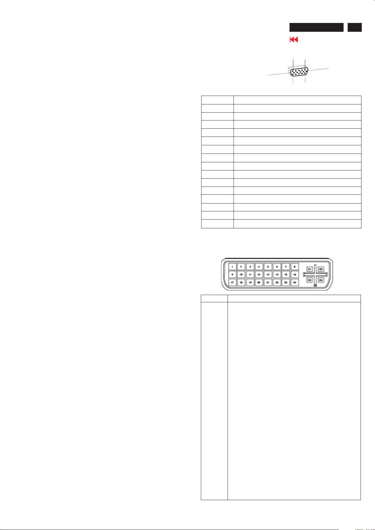
Pin Assignment
D-Sub connector
10
Pin No. Assignment
1 Red video input
2 Green video input / Sync On Green
3 Blue video input
4 Sense (Ground)
5 Cable detect
6 Red video ground
7 Green video ground
8 Blue video ground
9 +5V
10 Sync. ground
11 Sense Ground
12 Bi-directional data
13 H/H+V Sync
14 V. Sync
15 Data Clock
15
1
5
6
11
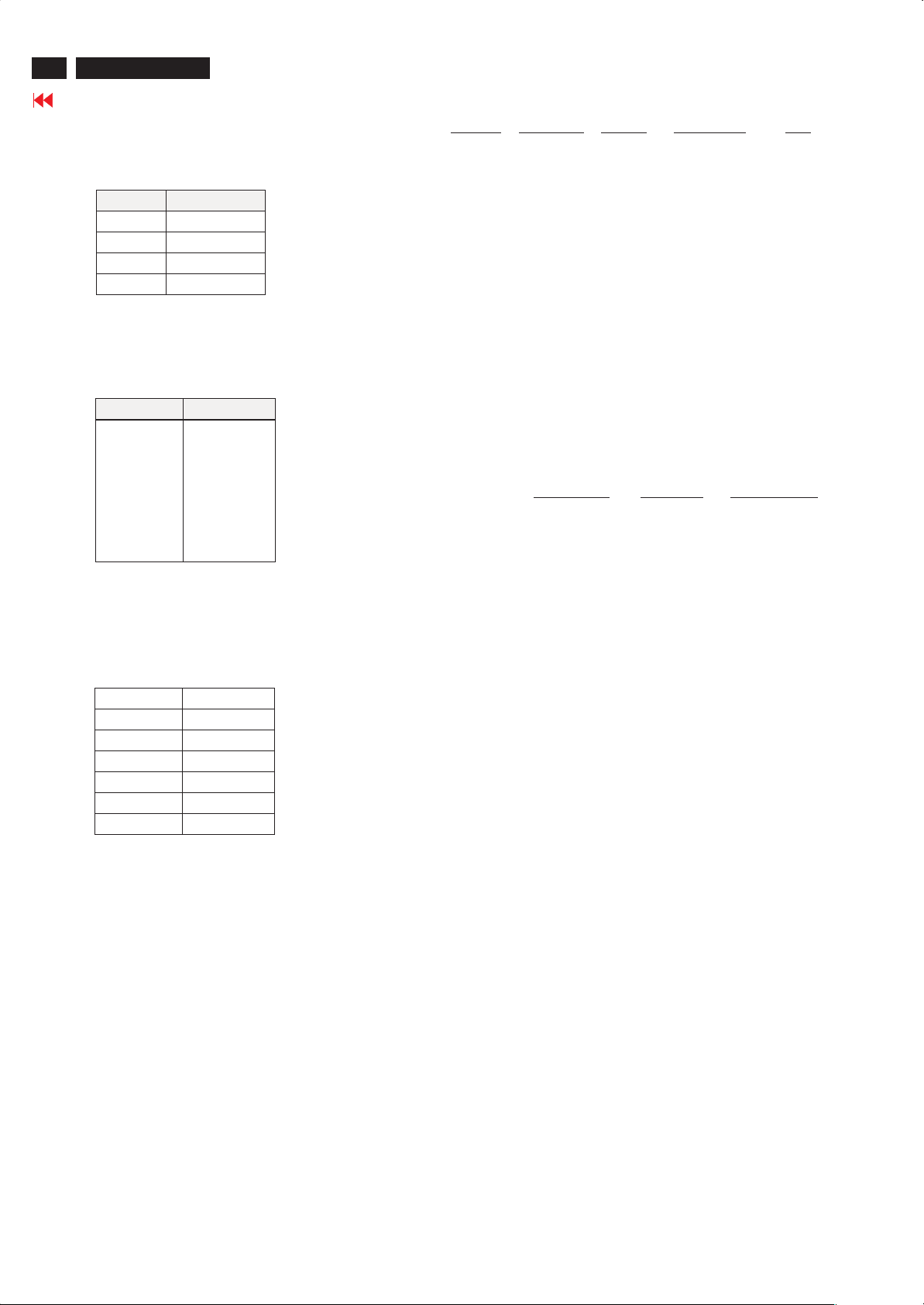
The digital/analog DVI-I connector contains 29 signal contacts
organized in three rows of eight contacts. Signal pin
assignments are listed in the following table:
3.0 Electrical characteristics
3.1 Interface signals
The input signals can be applied in three different modes :
1). D-shell Analog
Input signal : Video, Hsync., Vsync
Video : 0.7 Vp-p, input impedance, 75 ohm @DC
Sync. : Separate sync
TTL level , input impedance 5k ohm terminate
Hor. sync Positive/Negative
Ver. sync Positive/Negative
Composite sync TTL level, input impedance 5k
ohm terminate (Positive/Negative)
Sync on green video 0.3 Vp-p Negative
(Video 0.7 Vp-p Positive)
2). Intel DVI Digital
Input signal : Single channel TMDS signal
3) CVBS Video : 1Vp-p,75 Ohm
4) S-Video :Y- 1Vp-p,75 Ohm
C- 0.3Vp-p,75 Ohm
5) Component Video
3.1.1 Interface
3.2.1 D-Sub Cable
Length : 1.8 M +/- 50 mm (fixed)
Connector type : D-sub male with DDC2B pin assignments.
Blue connector thumb-operated jack screws
Pin No.
Description
1 TMDS data22 TMDS data2+
3 TMDS data2 shield
4NC
5NC
6 DDC clock
7 DDC data
8 Analog V-sync
9 TMDS data110 TMDS data1+
11 TMDS data1 shield
12 NC
13 NC
14 +5V
15 Ground(return for +5V and H/Vsync)
16 Hot plug detect
17 TMDS data018 TMDS data0+
19 TMDS data0 shield
20 NC
21 NC
22 TMDS clock shield
23 TMDS clock+
24 TMDS clock-
C1 Analog R
C2 Analog G
C3 Analog B
C4 Analog H-sync
C5 Analog GND (Analog R, G, Breturn)
Page 4
4
HP L2335
Technical Data(Continued)
Go to cover page
CVBS
The input signals are applied to display through CVBS cable
pin assignment
PIN NO. SIGNAL
1 GND
2 CVBS
3 CVBS
4 CVBS
STATUS Horizontal Vertical Power Spec LED
On Pulse Pulse < 100W Green
Stand-by No Pulse Pulse < 3 W Amber
Suspend Pulse No Pulse < 3 W Amber
off No Pulse No Pulse < 3 W Amber
According to VESA power saving signalling.
TCO92 power saving requirement
EPAenergy star requirement
4.0 Unit dimension / Weight
Set dimension (incl. pedestal): 542(W) * 531(H) * 210(D) mm
Net weight : : 10.1 KG
S-Video
The input signals are applied to display through S-Video cable
pin assignment
PIN NO. SIGNAL
1GND
2GND
3GND
4GND
5GND
6LUMA
8 CHROMA
Component Video
The input signals are applied to display through Component Video
Pin assignment
PIN NO. SIGNAL
1 GND
2 Red à Pr
3 GND
4 Blue à Pb
5 GND
6 Green àY
4.1 Tilt and swivel base
Tilt angle: Forward -5 to backward +25
Swivel angle : L / R 35
4.2 Transportation packages
4.3 Shipping dimension/Weight
Carton dimension : 685(W) X 335(H) X 655(D) mm
Gross weight : 14.0 KG
4.4 Block unit / Palletization
layers/block sets/layer sets/block unit
A TYPE 6 4 24
B TYPE 6 2 12
3.3.3 Horizontal scanning
3.3.4 Vertical scanning
3.4 Power input connection
3.5 Power management
Sync polarity : Positive or Negative
Scanning frequency : 30 - 107 K Hz
Sync polarity : Positive or Negative
Scanning frequency : 48 - 85 Hz
Power cord length : 1.8 M
Power cord type : 3 leads power cord with
protective earth plug.
The power consumption and the status indication of the set
with power management function are as follows,
Note : Disconnect DVI signal cable and audio module
Page 5

Connection to PC
S etTin g U p t h e Monitor
To set up the monitor, ensure that the power is turned off to the
monitor, computer system, and other attached devices, then
follow these steps:
1. Place the monitor in a convenient, well-ventilated location
near your computer.
2. Connect one end of the monitor signal cable to the video
connector on the rear panel of the computer, and the other end
to the back of the monitor.
3. Connect the power cable to the back of the monitor, and the
other end of the power cable to an electrical wall outlet.
HP L2335
Go to cover page
Re movi n g th e M on i t or B as e
You can remove the monitor base to mount the monitor on a wall,
swing arm, or other mounting fixture. Read the caution and
warning statements below before beginning the procedure.
5
4. Adjust the monitor as needed for your comfort using the
monitor s tilt, swivel, and height adjustment capabilities.
Moun tin g th e Monitor
1. Remove the monitor base. Refer to R e moving the Monitor
Base steps in the previous section.
When the base is removed, four threaded mounting holes are
exposed on the monitor panel to be used for mounting
purposes. These mounting holes are spaced 100 mm apart
and are compliant with the Video Electronics Standards
Association (VESA) standard for mounting flat panel
displays.
2. Mount the monitor to a swing arm or other mounting fixture
by following the instructions included with the mounting
fixture to be used.
Page 6
6
HP L2335
Go to cover page
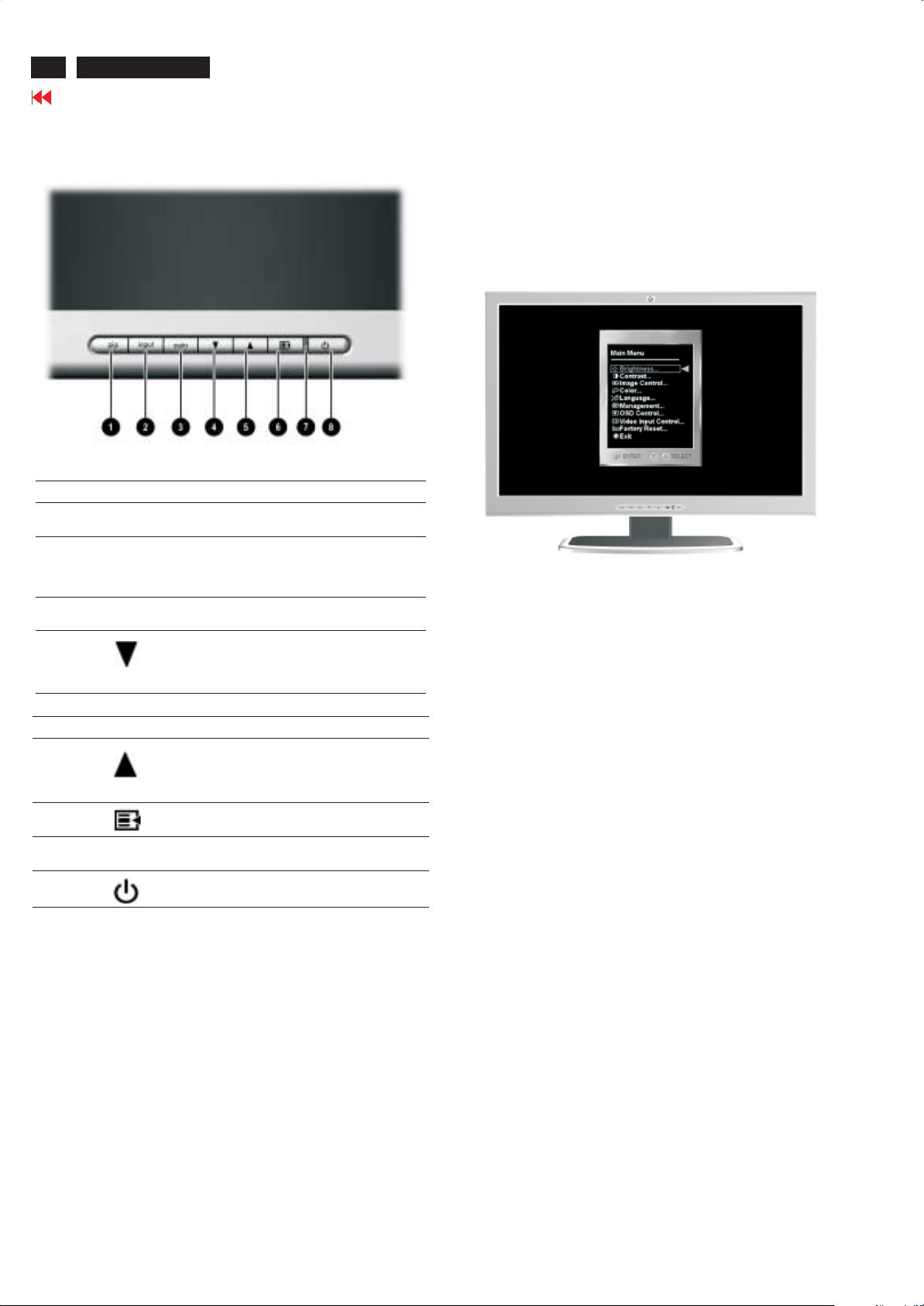
Front Panel Components
Fr on t P an el Compon en ts
N o. I con Contr o l Fu nction
1 PiP PiP button A ctivates Picture in Picture (PiP)
2 input Si gnal Input
button
3 auto Auto button A uto adjustmentofdisplayed
4 OSD A dj ust Select and adjust the OSD Menu
wi ndow
Si gnal input selection - scr olls
through VGA, DVI-A nalog,
DVI-Digital, Super video, and
composite video input
image
settings
Selects VGA in put when OSD is
not active
Adj u s tin g Monitor Set tin gs
Press the Menu button on the front panel of the monitor to view
the On Screen Display (OSD) Menu. The Main Menu window
pops up and you can make adjustments to your monitor s various
features. Use the left, right, up, and down arrow keys to make
your adjustments within the menu.
N o. I con Contr o l Fu nction
5 OSD Adjust Select and adjust the OSD Menu
6 Menu button Launches the On-Scr een Display
7 Power LE D Full pow er = Green
8 Power Switch Turns the monitor on and off
settings
Selects DVI-I input when OSD is
not active
(OSD) menu and selects func tions.
Sleep = Amber
Page 7

OSD User Mode
HP L2335
Go to cover page
7
Using the On -Sc r een Dis play
The adjustments for screen settings are located in the on-screen
display (OSD). Press the Menu button on the monitor's front
panel to view the OSD menu in one of six available languages.
The following table shows the menus and their functions at each
level:
OSD M en u Levels
Me nu Lev el1Me nu Lev el2Me nu Lev el3Me nu Lev el
4
Brightness Adj ustment
Contrast Adjustment
Image Control A uto
Co lor 9300K
Language Deutsch
Scale
Scale
Adjustme nt
Horizontal
Positi on
Ver ti cal
Positi on
Custom
Scaling
Sharpness Adjustment
Clock Adjustment
Clock Phase Adjustment
6500 K - sRGB
CustomColor Red, Green,
VideoColor Hue,
Espa ol
Adjusting
Message
Adjustment
Scale
Adjustment
Scale
Fi ll to S creen
Fill to Aspect
Ratio
One to One
Scale
Scale
Scale
Blue
Saturation
OSD M en u Levels
Me nu Lev el1Me nu Lev el2Me nu Lev el3Me nu Lev el
4
Francais
Italiano
Nederlands
Management Power S aver O n/Off
Power O n
Recall
Mode Dis play On/Off
Serial Number (display serial
Sleep T imer Set current&
Basic Menu
OSD Control H o ri zontal
VideoInput
Co ntrols
Positi on
Ver ti cal
Positi on
OS D TimeoutAdjustment
OS D
Tr ansparenc y
VideoInput
Select
Selection
On/Off
Selection
Selection
number)
sleep time
Adjustment
Scale
Adjustment
Scale
Scale
Adjustment
Scale
Analog (VGA)
Analog (DVI)
Digital (DVI)
S -Vi deo
OSD M en u Lev els
Me nu Lev el1Me nu Lev el2Me nu Lev el3Me nu Lev el
4
Co mposite
Co mposite
Auto Detect
Pi P Cont rol PiP Source Super Video
Co mposite
Co mposite
PiP S ize Pi P O ff
Horizontal
Positi on
Ver ti cal
Positi on
Facto ry Reset Yes
No
Exit
Video
Video
Video
Video
Small
Medium
Large
Adj Scale
Adj Scale
Page 8
8
HP L2335
OSD Lock/Unlock, Service Mode
Go to cover page
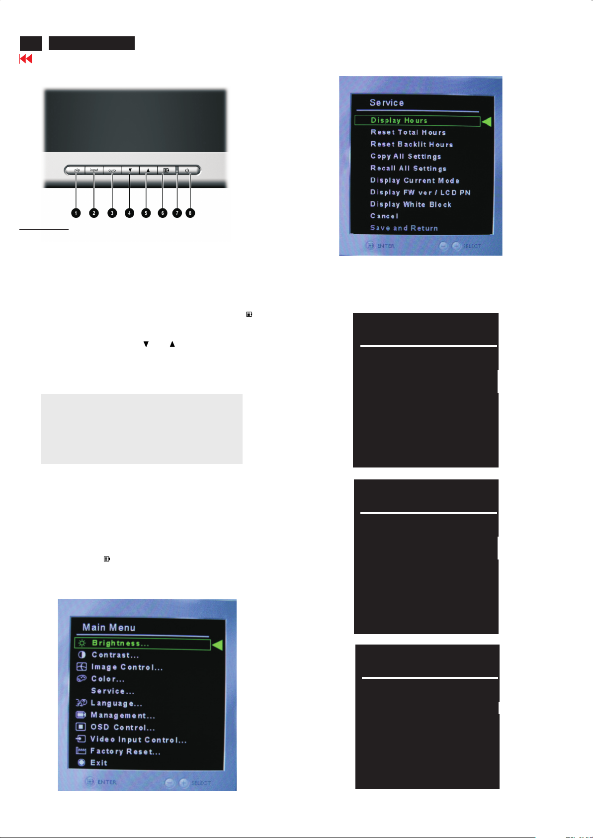
Front control panel
OSD Lockout
The OSD functionality shall be enabled or defeated with the following
button press sequence:
Input Select Control + Menu Select Control + Power-On Control
The OSD function can be locked by pressing Menu + input +
power on for more than 10 seconds, the screen shows following
windows for 3 seconds. Everytime when you press or
button, this message appears
On the screen automatically. The & (brightness) ,
AUTO
INPUT
Selecting , and
Firmware ver / LCD PN
Additional third level screens are given in the next section.
Display Hours Display Current Mode Display
gives the screens shown below.
Hours
(input) hotkey are still functional for brightness and input signal
selection while OSD locked.
OSD Lockout
Locked OSD function can be released by pressing Menu + Input +
power on button for more than 10 seconds again.
Access Service Mode (in USER MODE)
Method 1:
Step 1: Press Menu button(held in) + Power off -> Power on for
More than 10 seconds .
Step 2: Press MENU" " button ..
Bring up message as below.
Leave service mode by simply turn off and on the power of monitor.
Total: 000157
Backlight: 000082
Display Current Mode
Resolution: 1600 x 1200
Horz Sync: 106.3 kHz
Vert Sync: 85.0 Hz
Display F/W ver/LCD PN
=======>
Firmware Revision:
LCD Part Number:
Page 9

OSD Lock/Unlock, Service Mode
HP L2335
Go to cover page
9
Selecting and confirming shall cause the
current set of user modes to overwrite the factory presets. After
this has been confirmed and saved, any future selection of Reset
from the OSD shall cause the new presets (the user modes
saved as presets) to be loaded.
Copy All Settings
Confirm Copy Settings
Overwrite Presets
Cancel
Selecting and confirming shall cause the
monitor to reload the original factory settings into the presets and
into the user modes. Therefore, there shall be a set of memory
locations to store the original factory presets, which shall never be
overwritten, and a set of locations storing the settings that can be
overwritten by selecting or
Settings
.
Recall All Settings
Copy All Settings Recall All
Main OSD Menus
Pressing the Menu Select button will activate the Main Menu; the
factory default is the Basic Main Menu illustrated below.
Selecting an item is accomplished by moving the orange outline
and cursor with the + and/or buttons. The selection bar shows
default setting when first entering OSD main menu. Exit turns
the OSD off.
Selecting Advanced Main Menu will enable the menu shown
below. Once the Advanced Main Menu is selected, this menu
will remain the default until Basic Main Menu is activated from
the Management Menu .
””
””
““
””
Advanced Main Menu
The Copy Settings and Recall Settings function will result in the
following actions:
Contrast is set to 80
Brightness is set to 60
Reset the Custom RBG colors to RP,BP,GP
Clear all User Modes that are stored in NVRAM
Auto Adjust is executed on the currently displayed mode
Confirm Recall Settings
Recall Original Presets
Cancel
Basic Main Menu
Selecting shall cause the monitor to display
a square white block, approximately 20% of the total area,
centered in the display. This block shall be displayed until the
Menu button is pressed, at which time the Service menu shall be
displayed again.
If a reset has been confirmed, then the item in
the second level menu shall be active and selected by default.
Otherwise, shall be selected by default.
Display White Block
Save and Return
Cancel
Selecting Auto Adjustment in either the Basic or Advanced
Main Menu will result in the activation of the image adjustment
process. During this activity, a message displaying Adjusting
will be displayed. For the DIGITAL mode, the following
selections will be disabled, displayed with black or dark gray text:
””
””
Page 10
10
HP L2335
Go to cover page
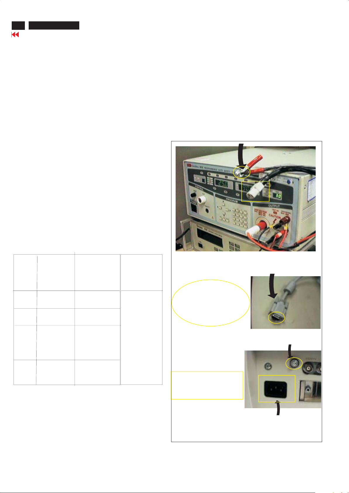
Safty Test Requirements
All units that are returned for service or repair must pass the
original manufactures safety tests. Safety testing requires both
and testing.Hipot Ground Continuity
HI-POT TEST INSTRUCTION
1. Application requirements
1.1 All mains operated products must pass the Hi-Pot test as
described in this instruction.
1.2 This test must be performed again after the covers have
been refitted following the repair, inspection or modification
of the product.
2. Test method
2.1 Connecting conditions
2.1.1 The test specified must be applied between the parallel-
blade plug of the mainscord and all accessible metal
parts of the product.
2.1.2 Before carrying out the test, reliable conductive
connections must be ensured and thereafter be
maintained throughout the test period.
2.1.3 The mains switch(es) must be in the "ON" position.
3. Equipments and Connection
3.1. Equipments
For example :
- ChenHwa 9032 PROGRAMMABLE AUTO SAFETY
TESTER
- ChenHwa 510B Digital Grounding Continuity Tester
- ChenHwa 901 (AC Hi-pot test), 902 (AC, DC Hi-pot test)
Withstanding Tester
3.2. Connection
* Turn on the power switch of monitor before Hipot and
Ground Continuity testing.
Clip
Clip
2.2 Test Requirements
All products should be HiPot and Ground Continuity tested as
follows:
Condition HiPot Test for HiPot Test for Ground Continuity
products where products where Test requirement
the mains input the mains input is
range is Full 110V AC(USA
range(or 220V type)
AC)
Test 2820VDC 1700VDC Test current:
voltage (2000VAC) (1200VAC) 25A,AC
Test time:
Test time 3 seconds 1 second 3 seconds(min.)
(min.) Resistance
required:
Trip set at 100 uA 5 mA <=0.09+R ohm,
current for Max. R is the
(Tester) limitation; set resistance of
at 0.1 uA for the mains cord.
Min. limitation
Ramp set at 2
time seconds
(Tester)
(ChenHwa 9032 tester)
Video cable
Connect the "video cable"
or "grounding screw"
to the CLIP on your tester.
Grounding screw
Connect the power cord
to the monitor.
2.2.1 The test with AC voltage is only for production purpose,
Service center shall use DC voltage.
2.2.2 The minimum test duration for Quality Control Inspector
must be 1 minute. No breakdown during the test.
2.2.3 The test voltage must be maintained within the specified
voltage + 5%.
2.2.4 The grounding blade or pin of mains plug must be
conducted with accessible metal parts.
4. Recording
Hipot and Ground Continuity testing records have to be kept for
a period of 10 years.
Power outlet
(Rear view of monitor)
Page 11
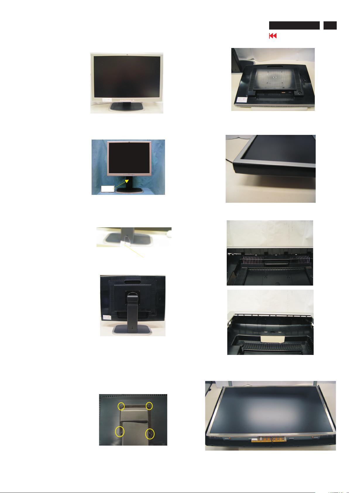
Front view as shown
in Fig. 1.
Fig. 1
Mechanical Instructions
HP L2335
Go to cover page
11
To use the height adjustment
Stand in Fig. 2.
Fig. 2
Step 1 :
Disconnect screw and push
up and down the the monitor
as shown in Fig. 3.
Stand
Disconnect screw
Fig. 3
Step 3 :
Remove Front Bezel by "-" screw driver on click holes to dig the back
cover as shown in Fig. 7.
Front Bezel==>
Fig. 7
Plastic clip (left & right) can be released by "-" screw driver as shown in
Fig.8&9.
Fig. 8
Fig. 6
Step 2 :
Lay the front bezel
1.
down
on a soft area to
prevent it from getting
scratched, defaced, or
broken.
2.Remove the four screws
as shown in Fig. 5.
3.Remove the monitor
base from the monitor
as shown in Fig. 5.
Fig. 4
4 SCREWs
Fig. 5
Fig. 9
Step 4 :
Remove front bezel as shown in Fig. 10.
Control panel ==>
Fig. 10
Page 12
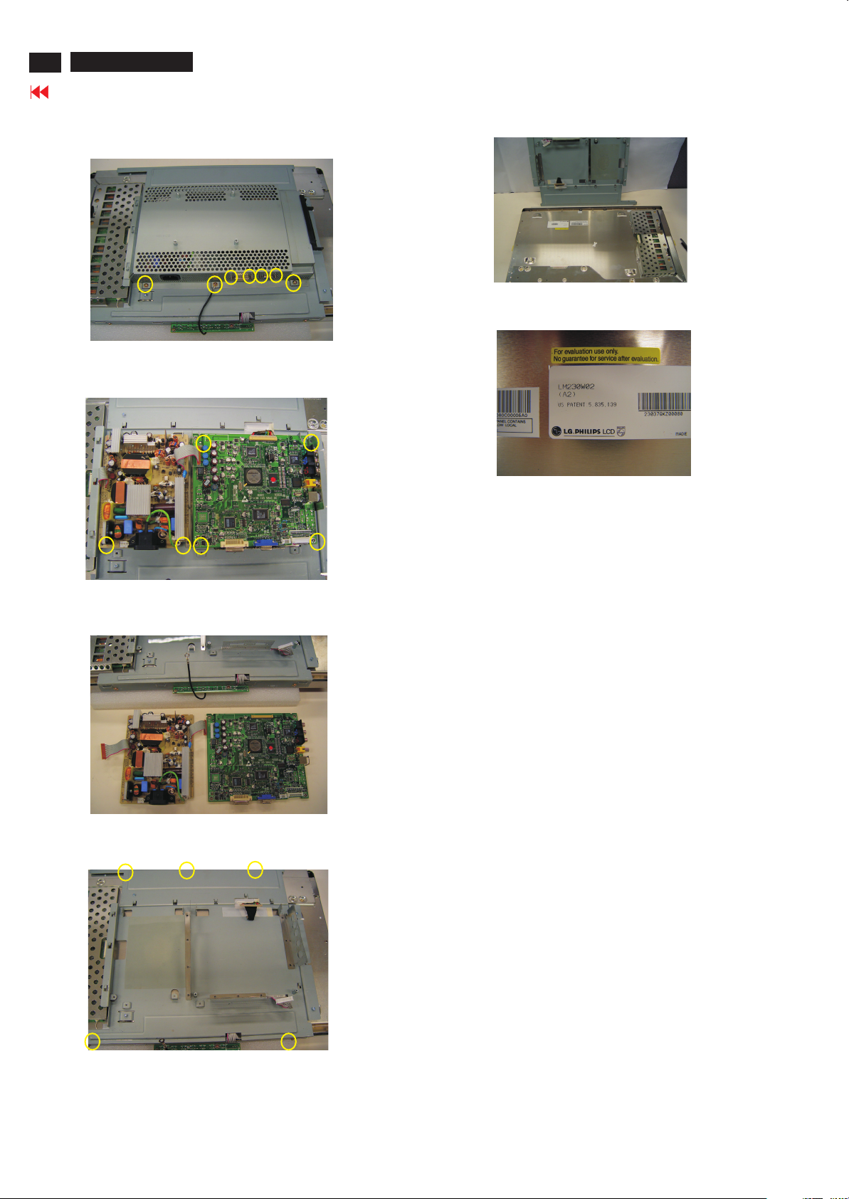
12
HP L2335
Mechanical Instructions (Continued)
Go to cover page
Step 6 :
1.Take out LCD panel from back cover as shown in Fig. 11.
Metal cover
Step 10 :
1.The Panel information as shown Fig.15~16.
.
Fig. 15
7 SCREWs
Fig. 11
Step 7:
Remove metal cover 3 screws and 4 Hexagonal Screws
as shown in Fig. 11.
Hexagonal screw
8101
8102
Fig. 12
Step 8 :
Remove power & scaler board as shown in Fig. 12~13
-Reomve the 6screws and Disconnedt 8101,8102,1551. Connector.
Fig. 16
1074 823827714381 TFT-LCD LC230W02
***************************************************************************
In warranty, it is not allowed to disassembly the LCD panel, even the
backlight unit defect.
Out of warranty, the replacment of backlight unit is a correct way
when the defect is cused by backlight (CCFL,Lamp).
***************************************************************************
Fig. 13
Step 9 :
Remove the Main Frame as shown in Fig. 14.
-Remove the 5 screws.
Fig. 14
Main Frame
5 SCREWs
Page 13
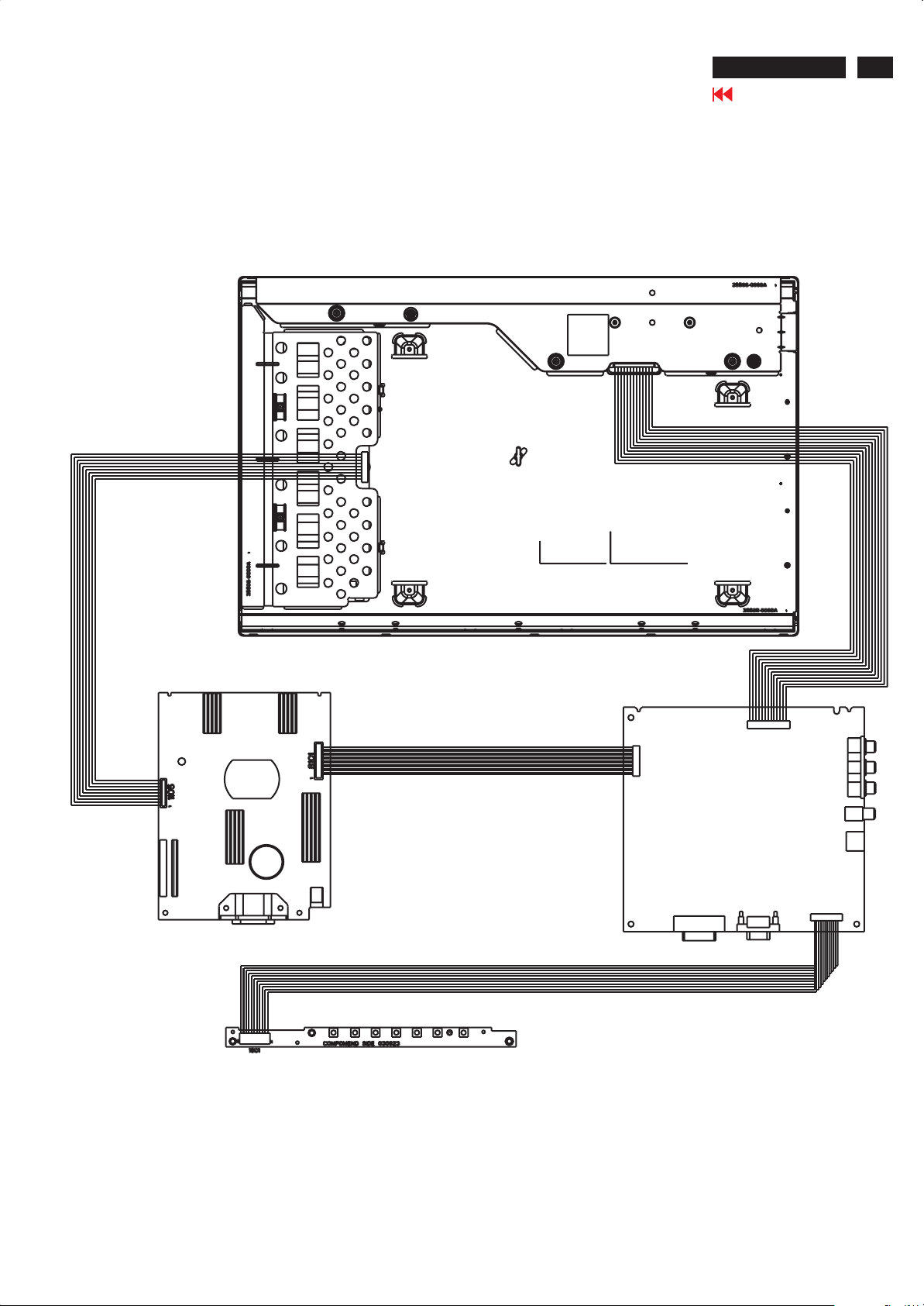
Wiring Diagram
HP L2335
Go to cover page
13
Page 14

14
HP L2335
Go to cover page
Factory mode Adjustment:
Display Adjustment , Aging Mode
Entering factory mode as Press and button
simultaneously and power ON as Fig. 1shown below.
Use buttons to Factory Mode to enter byMenu then
appearFig.2 as below
Menu auto
9300KRGB
6500KRGB
Color temperature gain adjustment. Use these menu items
to adjust the RGB gains of pre-amp for different color
temperatures, ranges from 0 to 255.
Access AGING Mode (Burn in mode) : IN Factory MODE
Step 1 :
Push Menu " " & " " buttons at the same time and power ONAuto
Step 2: Disconnect Interface (Signal) cable.
=> Bring up
"Full black pattern (if black, wait 5 seconds
around)"
"Full White pattern with character "Aging"
or
as below.
Use buttons to Factory Mode to enter byMenu then
9300K For CAD/CAM,6500K For IMAGE MANAGEMENT,
ORIGINAL PANEL COLOR,AUTO COLOR ADJUST.
Bring up
After 5 seconds, bring up :
After 5 seconds, bring up :
:
Aging
Aging
After 5 seconds, bring up :
----------
----------Repeatly
How to return to Normal display (User Mode)
Method : reconnect the interface cable of LCD monitor.
Page 15
1. General points
Electrical instructions
13 61.80 SUN WS 1152x900 65.96
HP L2335
Go to cover page
15
1.1 During the test and measuring, supply a distortion free AC
mains voltage to the apparatus via an isolated transformer with
low internal resistance.
1.2 All measurements mentioned hereafter are carried out at a
Normal mains voltage (90 - 132 VAC for USA version, 195 -264
VAC for EUROPEAN version, or 90 - 264 VAC for the model with
full range power supply, unless otherwise stated.)
1.3 All voltages are to be measured or applied with respect to
Ground, unless otherwise stated.
Note: don't use heat-sink as ground.
1.4 The test has to be done on a complete set including LCD panel
in a room with temperature of 25 +/- 5 degree C.
1.5 All values mentioned in these test instruction are only applicable
of a well aligned apparatus, with correct signal.
1.6 The letters symbols (B) and (S) placed behind the test
instruction denotes (B): carried out 100% inspection at
assembly line
(S): carried out test by sampling
1.7 The white balance (color temperature), has to be tested in
subdued lighted room.
1.8 Repetitive power on/off cycle are allowed.
1.9 All optical characteristics (including WHITE-D, Brightness, and
so on) are determined according to panel specification after
warming up approximate 30 minutes that brightness stability is
optimal, and follow strictly after panel specification.
2. Input signal
Signal Type
2.1.1 Analog Video: 0.7 Vp-p linear, positive polarity
Sync. : TTL level, separate, positive or negative polarity
Signal source : pattern generator format as attachment.
( Table 1 to 53 ) Reference generator : Quantumdada 802G
2.1.2 Digital Video : 600m Vp-p TMDS signal
2.1.3 CVBS Video : 1Vp-p, 75Ohm
2.1.4 S-Video : Y-1 Vp-p, 75 Ohm
2.2 Input signal Mode
Item H.Freq.
(KHz)
C-0.3V
p-p, 75 Ohm
Factory Preset Modes (25 modes)
Mode Resolution V.Freq.
(Hz)
1 31.469 IBM VGA 3H 720x400 70.087
2 31.469 IBM VGA 2H 640x480 59.940
14 60.00 VESA 1280x960 60.00
15 63.981 VESA 1280x1024 60.020
16 79.976 VESA 1280x1024 75.025
17 91.1 VESA 1280x1024 85
18 75.0 VESA 1600x1200 60
19 93.8 VESA 1600x1200 75
20 74.038 CVT
1920x1200 59.95
2.30MA-R
21 74.52 CVT 2.30MA 1920x1200 60
22 44.86 CVT 0.83MA 1152x720 60
23 47.74 CVT 0.94MA 1224x768 60
24 65.29 CVT 1.76MA 1680x1050 60
25 69.828 CVT 0.93MA 1728x1080i 60
3. AC, DC Adaptor
3.1 Set mains voltage at 90Vac
Plug in the mains cable, check the display picture should be
normal. Plug the mains cable in and out at random, the display
picture should be normal again.
3.2 Set mains voltage at 264Vac
Plug in the mains cable, check the display picture should be
Normal. Plug the mains cable in and out at random, the display
picture should be normal again.
4. Display Adjustment
4.1 Input signals check In factory mode, use 64 gray level and
set the R,G,B gain to 100%.
4.2 Display quality test
Use timing mode as describe in 2.2, and use the pixel on / off
Pattern to adjust the clock until no stripe and adjust the phase
until clear picture. Check all factory presetting 25 modes.
4.2.1 SOG mode test : Use following timing for SOG test
64 KHz/60Hz, 1280 X 1024, pixel=108 Mhz
3 37.90 IBM VGA 640x480 72.00
4 37.500 VESA 640x480 75.000
5 43.27 VESA 640x480 85.01
6 37.879 VESA 800x600 60.317
7 53.67 VESA 800x600 85.06
8 49.700 MACINTOSH 832x624 75.000
9 48.363 VESA 1024x768 60.004
10 60.023 VESA 1024x768 75.029
11 68.68 VESA 1024x768 85.00
12 68.700 MACINTOSH 1152x870 75.000
Horizontal Vertical
Frame border =0 Frame border =0
Total size =15.620 s Total size =16.670 ms
Display size =11.852 s Display size =16.000 ms
Rear porch = 2.000 s Rear porch = 0.580 ms
Sync width = 1.000 s Sync width = 0.080 ms
Sync polarity = - Sync polarity = -
Sync on green
4.5 OSD Control Factory Default Values The OSD Controls
shall have the following factory default values:
1. Menu = Basic
2. Brightness = 90
3. Contrast = 80 (with no saturation visible at 85)
4. Color Temperature = 6500K for the Commercial and
Custom Color for Consumer models.
5. Language = English
6. Power Saver = ON
7. Power On Recall = ON
8. Mode Display = OFF
9. Horizontal OSD Position = 50
10. Vertical OSD Position = 50
11. OSD Timeout = 30
Page 16

16
HP L2335
HP L2025
Firmware upgrade for CPU
Go to cover page
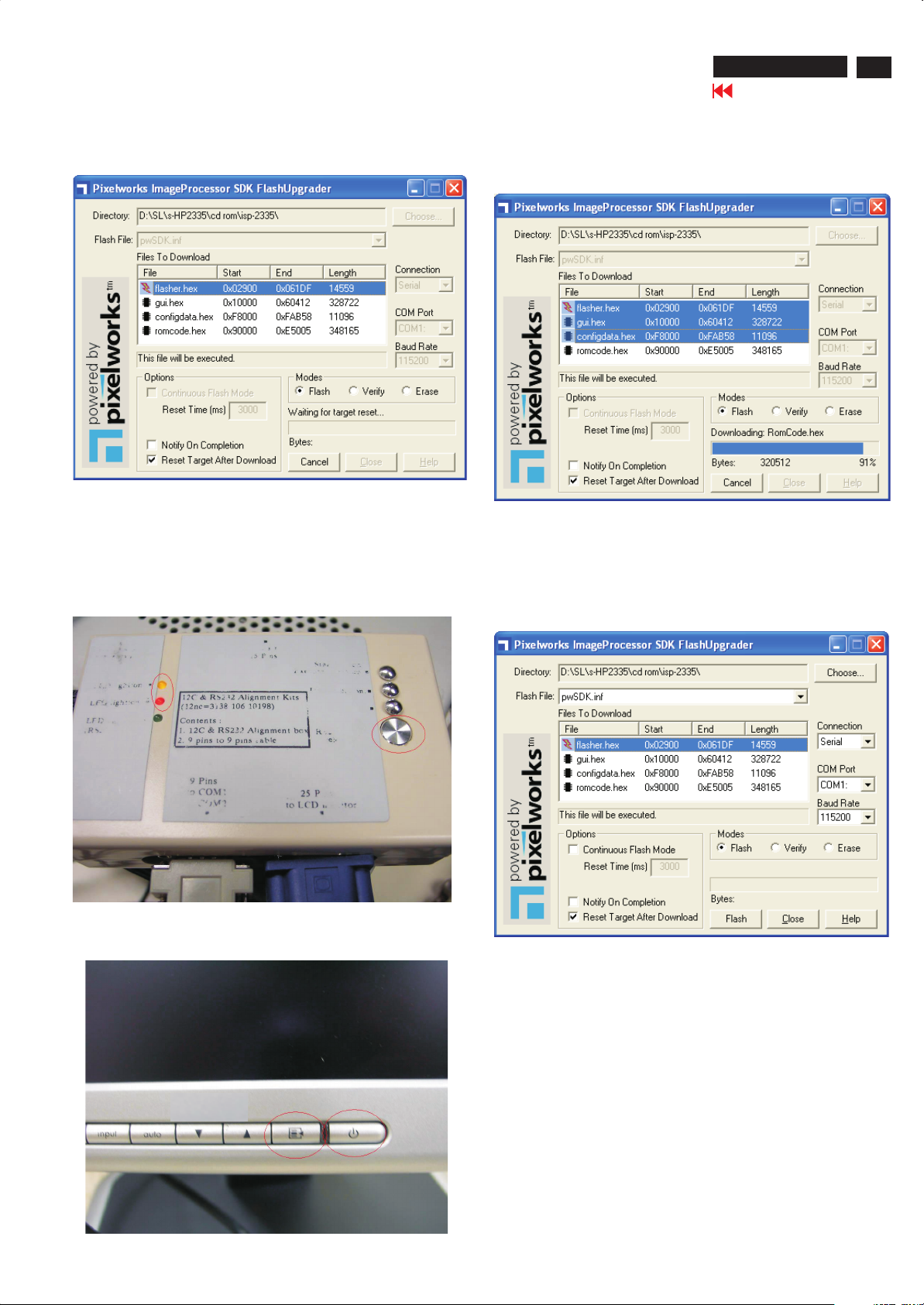
Configuration and procedure
There is an application software to upgrade the firmware of CPU.
Bootcode of CPU should be embeded into CPU in production line
before you use those application (.exe) file.
Flashupgrader.exe => for Win95, 98 & ME
FlashupgraderNT.exe => for Win2000, NT & XP
CPU software=>Flashupgrader.exe or FlashupgraderNT.exe
I2C & RS232 Alignment KITs(3138 106 10198)
RS232 cable(9pins to 9pins) as below
Fig. 1 => Connection for Firmware upload.
** Do not connect Mains cord to Monitor at this moment. **
OPTIONAL TOOL
I2C & RS232 Alignment Kits --------------------->
(3138 106 10198)
9 pins to 9 pins cable
connect to PC com port
D-sub cable
connect to HP L2335 monitor D-sub port
--------------------------------------------------->
----------------------->
PC
Fig. 1
Monitor-HP L2335
Fig. 3
Check Firmware version : example as below.
CODE VERSION. 0.22 2003-07-29
CONFIG VERSION. 0.22 2003-07-29
OSD VERSION. 0.22 2003-07-29
The updated firmware of CPU => as shown
in Fig. 4
1.Configdata.hex 2.Flasher.hex 3.Gui.hex 4.romcode.hex
5.pwSDK.inf 6.Flasupgrader.NT.exe in Fig. 4
Monitor (A)
Connect to
Mains cord
Video cable
Connect the PC Com port
to Alignment kits
To video card
Connect the HP L2335 D-sub cable
to Alignment kits
Do not Connect to Mains cord
at this moment.
------------------------------->
Factory mode Adjustment:
Entering factory mode as Press and button
simultaneously and power ON as Fig. 1shown below.
Menu auto
D-Sub
Execution files => as shown in Fig. 4
1.Make sure FlashUpgrader or FlashUpgraderNT is placed in the
same directory with *.hex files and pwSDK.ini
2.There two versions of FlashUpgraders for different Windows
operating systems.
Flashupgrader.exe => for Win95, 98 & ME
FlashupgraderNT.exe => for Win2000, NT & XP
Remove the AC power cable of HP L2335 monitor
3.
4. After double icon, you will see this
window:
clicking the FlashUpgrader
Use buttons to Factory Mode to enter by Menu then
appear Fig.2 TO SEE CODE VERSION as below
Page 17
Firmware upgrade for CPU (Continued)
HP L2335
HP L2025
HP L2025HP L2025
Go to cover page
7
25
17
5. Make sure you choose the path of the files.
6. You will see the following screen
FlashUpgrader is waiting for the AC reset signal.
7.Make sure the I2C & RS232 switch (the circled button at the
right hand side of the following photo) of the communication box
is held down, the orange and the red LEDs light on while the other
green LED is off.
Then click Flash
9. Hold the two function keys and connect the AC cable.
The download progress should automatically start. When you see
a running progress bar like the diagram below, you may release
the two function keys.
10. When the download progress is completed, you may see the
FlashUpgrader like this:
Connect the box to the serial port of your PC via RS232 cable and
to the monitor via D-SUB cable.
8. Press the power and the menu key of the monitor at the same
The monitor will automatically be reset and you may confirm the
version number in the service menu.
PS. If the download does not start, reseting the power of the
communication box or restarting Windows may solve the
problem.
Page 18

HP L2025
18
HP L2335
Go to cover page
DDC Instructions
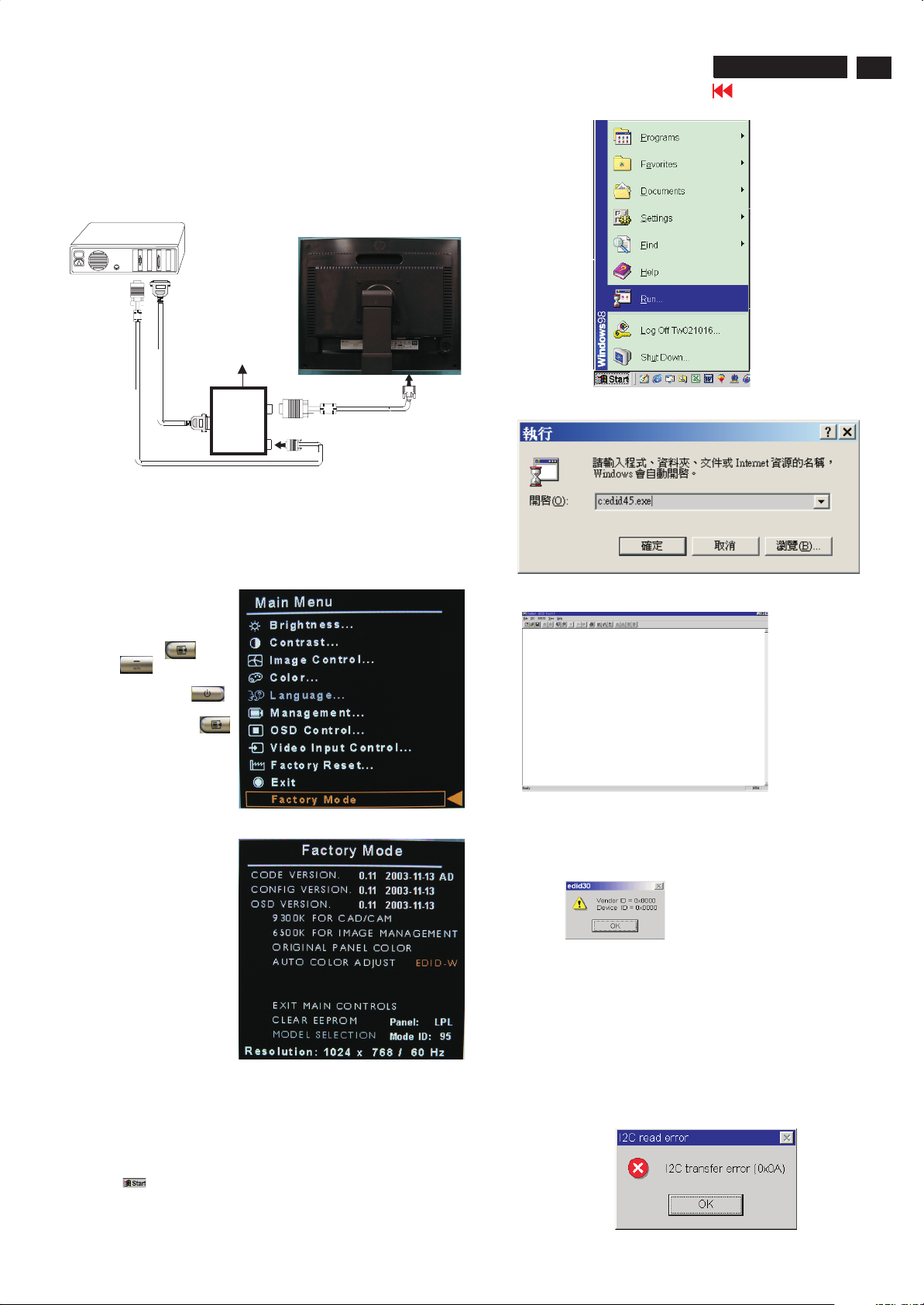
General
DDC Data Re-programming
In case the DDC data memory IC or main EEPROM which storage all
factory settings were replaced due to a defect, the serial numbers have
to be re-programmed" ".
Analog DDC IC, & EEPROM
It is advised to re-soldered DDC IC and main EEPROM from the old
board onto the new board if circuit board have been replaced, in this
Case the DDC data does not need to be re-programmed.
Additional information
Additional information about DDC (Display Data Channel) may be
obtained from Video Electronics Standards Association (VESA).
Extended Display Identification Data(EDID) information may be also
obtained from VESA.
System and equipment requirements
1. An i486 (or above) personal computer or compatible.
2. Microsoft operation system Windows 95/98 .
Y o Install the EDID_PORT_Tool under Win2000/XP . As
ou have t
Fig. 1 .
Note: The EDID45.EXE is a windows-based program, which cannot be
run in MS-DOS.
Note: The alignment box has already build-in a batteries socket for
batteries (12V)
using as power source. Pull out the socket by
remove four screws at the rear of box. Please do not forget that
remove batteries after programming. The energy of batteries can
only drive circuits for a short period of time.
To Printer
DC 8V~12V
Power
indicator
To Monitor
Video CardVideo Card
A/D Alignment Kits - Analog connectionA/D Alignment Kits - Analog connection
Pin assignment
A. 15-pin D-Sub Connector
Pin
Assignment
No.
1 Red video input 9 DDC +5V supply from pc
2 Green video input /SOG 10 Sync GND
3 Blue video input 11
4 12 Bi-directional data
Ground
5
Cable detect
6 Red video ground 14 V. Sync
7 Green video ground 15 Data clock
8 Blue video ground
A/D Alignment Kits - Digital connectionA/D Alignment Kits - Digital connection
Pin
Assignment
No.
Ground
13 H. + V. Sync
A. Cody the "UserPort.sys" to C:\WINNT\system32\drivers(win2000)
C:\WINDOWS\system32\drivers(winXP)
B. Running " io.exe" everytime, Before you start to programming
edid data .
3. EDID45.EXE program .
4. A/D Alignment kits (3138 106 10079):
inclusion : a. Alignment box x1 (as Fig. 2)
Fig. 1Fig. 1
B. 29-pin DVI Cable Connector
Description
Pin
1 T.M.D.S. data2-
2 T.M.D.S. data2+
3 T.M.D.S. data2 shield
4 No Connect
5 No Connect
6 DDC clock
7 DDC data
8 Analog V-sync
9 T.M.D.S. data1-
10 T.M.D.S. data1+
11 T.M.D.S. data1 shield
12
No Connect
13 No Connect
14 +5V Power
15 Gnd (for +5V)
H/V sync
Description
Pin
16 Hot plug detect
17 T.M.D.S. data0
18 T.M.D.S. data0+
19 T.M.D.S. data0 shield
20 No Connect
21 No Connect
22 T.M.D.S clock shield
23 T.M.D.S. clock+
24 T.M.D.S. clock
C1 Analogy R
C2
Analogy G
Analogy B
C3
Analogy H-sync
C4
Analogy GND
C5
-
-
(RGB return)
Configuration and procedure
There are threeips contained serial number on the circuit board,
Analog DDC IC (7225), Digital DDC IC (7223,7224) and main
EEPROM (7472) which storage all factory settings. Following
descriptions are the connection and procedure for Analog DDC
IC and Digital DDC IC, the main EEPROM can be reprogrammed along with Analog IC by enable factory memory
data write function on the DDC program (EDID45.EXE).
b. Printer cable x1
c. (D-Sub) to (D-Sub) cable x1
Fig. 2Fig. 2
In order to avoid that monitor entering power saving mode due to
sync will cut off by alignment box, it is necessary to initialize
alignment box before running programming software (EDID45.EXE).
Following steps show you the procedures and connection.
Initialize alignment box
Page 19
DDC Instructions
Step 1: Supply 8~12V DC power source to the Alignment box by
plugging a DC power cord or using batteries.
Step 2: Connecting printer cable and video cable of monitor as Fig. 4
Step 3: Run the EDID45.EXE program until the main menu appears.
This is for initialize alignment box.
HP L2025
HP L2335
HP L2025
HP L2025
Go to cover page
25
7
19
PC
DC Power
8~12 V
~
~
To video card
Fig. 4
Re-programming DDC IC
Step 1: After initialize alignment box, connecting all cables and box as
Fig. 4
Step 2: Enter Factory mode to select EDID-W as Fig. 4 -1. 4 -2
Step 3: Follow the steps on DDC re-programming instructions to staring
re-programming.
To printer port (LTP1)
Printer
Port
To
Monitor
To P C
D-Sub connector
1.D-SUB connector
1
Access Factory Mode
Power off the monitor,
To hold And
+AUTO buttons at the
same time ,
And press
button to power on the
monitor. Press
button to bring up OSD
menu for selecting EDID-W
as Fig, 4-2
MANU
POWER
MANU
3. At the submenu, type the letter of your computer's floppy disk drive
followed by :EDID45 (for example, A:\EDID45.exe,)as shown in Fig. 6.
Fig. 6
4. Click button. The main menu appears (as shown in Fig. 7).OK
This is for initialize alignment box.
Fig. 7
====>
Factory Mode indicator
Fig. 4-2
Fig. 4-1
Re-programming Analog Device As Fig. 4
DDC re-programming instructions
Start on DDC program
Start Microsoft Windows.
1. Insert the disk containing EDID45.EXE program into floppy disk drive.
2. Click , choose Run at start menu of Windows 95/98.
Note:
If the connection is improper, you will see the following error
message before entering the main menu. Meanwhile, the
(read EDID) function will be disable. At this time, please make
sure all cables are connected correctly and fixedly, and the
procedure has been performed properly.
Fig. 8
Note 2: During the loading, EDID45.1 will verify the EDID data which
just loaded from monitor before proceed any further function,
once the data structure of EDID can not be recognized, the
following error message will appear on the screen as below.
Please confirm following steps to avoid this message.
1. The data structure of EDID was incorrect.
2. DDC IC that you are trying to load data is empty.
3. Wrong communication channel has set at configuration setup
windows.
4. Cables loosed or poor contact of connection.
Page 20

20
HP L2335
Go to cover page
DDC Instructions
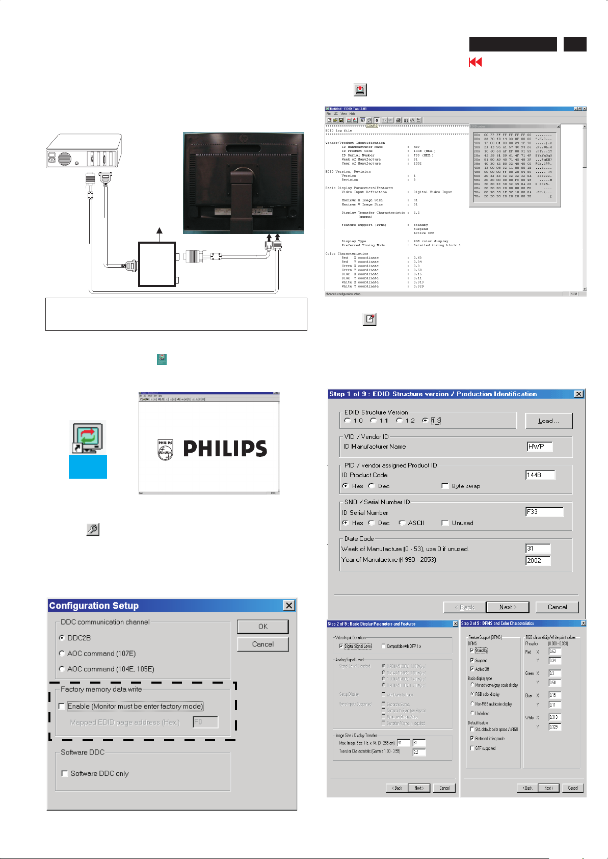
Step 2: Read DDC data from monitor
1. Click icon as shown in Fig. 12 from the tool bar to bring up
the Channels "Configuration Setup" windows as shown in Fig. 10.
2. Select the DDC2Bi as the communication channel.
As shown in Fig. 10.
Fig. 10
3. Click OK button to confirm your selection.
4. Click icon (Read EDID function) to read DDC EDID data from
monitor. The EDID codes will display on screen as shown in Fig. 11.
Modify DDC data (Serial No.)
1. Click icon on the tool bar.
2. Click till the Step 9 of 9 window appears.
3. Type the new Serial No. (for example, TWP335Z001).
4. Click till the last step window appears, then click to
exit the Step window.
Attention :
Before doing "SerialNumber.exe" in your windows 98 PC, The HPL2335 monitor
must be in the factory mode, then run following process as below.
Step 1: Double click "SerialNumber.exe"
Bring up: Fig. 14
Fig. 14
Fill out serial number of monitor.
For example "TWP335Z001" as shown in Fig. 15.
Write DDC data to monitor
1. Click icon from the tools bar to starting rewrite DDC data.
2. Click for confirmation.
3. In order to match the same serial number in OSD with DDC data,
The following action should be executed.
*****************************************************************************
Change/update the serial number which should be proceeded
by application software "SerialNumber.exe" as shown in Fig. 12
*****************************************************************************
Fig. 12
*****************************************************************************
Connection :Using IIC & Rs232 Alignment Kits(3138 106 10198)
for Serial Number applicationFig.13.
*****************************************************************************
Monitor (A)
PC
25 pins
Com1 or
Com2
9 pins
Monitor (B)
Rear view of HP L2335
Fig. 11
---------------->
Fig. 15
(click "Serial Number")
Step 2: Click "Serial Number" as shown in Fig. 16.
---->
Fig. 16
(Com port for application)
Bring up Fig. 16 with "57600,n,8,1 Com1"
Step 3: Verify "Serial Number" by OSD as shown in Fig. 17.
Press OK button
=>select "management"
=>press OK Button,then
=>select "Serial Number"
=>press OK Button
Bring up :
Fig. 17 for verification.
TWP335Z001
Connect to
Mains cord
Video cable
To video card
To Com1 or Com2 (PC)
9 pins
Fig. 17
Fig. 13
Page 21
DDC Instructions (Continued)
HP L2335
Go to cover page
21
Re-programming Digital DDC IC
Connecting all cables and alignment box as shown in
Step 1:
Fig. 18.
1=DVI-I connector
PC
DC Power
8~12 V
~
~
To video card
Fig.18
After connection for Digital DDC application, if it is still in Analog DDC
application of EDID301.
Exit EDID45 program before Digital DDC application.
Step 2: Initialize alignment box
(Shortcut of EDID301.EXE on
Double click EDID301 icon (as shown in Fig. 19) which is
on the screen of Windows Wallpaper.
Bring up main menu of EDID45 as shown in Fig. 20.
To printer port (LTP1)
Printer
Port
DVI-I to D-Sub cable
To
Monitor
To P C
D-Sub connector
Windows Wallpaper already.)
1
2=D-SUB connector
2
1
4. Click icon (Read EDID function) to read DDC EDID data from
monitor. The EDID codes will display on screen as shown in Fig. 23.
Fig. 23
Step 4: Modify DDC data (verify EDID version, week, year)
1. Click (new function) icon from the tool bar, bring up
Step 1 of 9 (Digital) as shown in Fig. 24 .
EDID301 DDC application provides the function selection and
text change (select & fill out) from Step 1 to Step 9.
Fig. 24
EDID
301.exe
1
Fig. 19
Step 3: Read DDC data from monitor
1. Click icon from the tool bar to bring up the Channels
Configuration Setup windows as shown in Fig. 21.
2. Select the DDC2B as the communication channel.
Disable "Factory memory data write" for Digital DDC
application
3. Click OK button to confirm your selection.
as shown in Fig. 22.
Fig. 20
Fig. 22
Fig. 25
Fig. 26
Page 22

HP L2335
22
HP L2025
Go to cover page
Fig. 27
DDC Instructions (Continued)
Step 6: Write DDC data
1. Click (Write EDID) icon from the tool bar to write DDC data.
2. Click (Read EDID) to confirm (check contents) it.
Step 7: Save DDC data
Sometimes, you may need to save DDC data as a text file for using
in other IC chip. To save DDC data, follow the steps below:
1. Click (Save) icon (or click "file"-> "save as") from the tool bar
and give a file name as shown in Fig. 33.
2. Click .Save
Fig. 28
HP L2335-digital
TWP335Z001
HP L2335-digital
Fig. 33
Fig. 29
Step 5: Modify DDC data (Monitor Serial No.)
Monitor S
TWP335Z001)
erial No. can be filled up or be changed (for example,
as shown in Fig. 30.
HPL2335
Fig. 31
Fig. 30
Step 8: Load DDC data
1. Click from the tool bar.
2. Select the file you want to open as shown in Fig 34.
3. Click .
Open
HP L2335-digital
HP L2335-digital
HP L2335-digital
Step 9: Exit DDC program
Pull down the File menu and select Exit as shown in Fig. 35.
Fig. 35
Fig. 34
Click to exit the Step window as shown in Fig. 22.Finish
Fig. 32
Page 23

DDC Data
HP L2335
Go to cover page
23
THE DISPLAY DATA CHANNEL ( DDC 2B ) CONTENT INCLUDING
(FOR HP L2335 ANALOG)
**********************************************************************
EDID log file
**********************************************************************
Vendor/Product Identification
ID Manufacturer Name : HWP
ID Product Code : 2614 (HEX.)
ID Serial Number : 1010101 (HEX.)
Week of Manufacture : 35
Year of Manufacture : 2003
EDID Version, Revision
Version : 1
Revision : 3
Basic Display Parameters/Features
Video Input Definition : Analog Video Input
0.700V/0.300V (1.00Vpp)
without Blank-to-Black Setup
Separate Sync
Composite Sync
Sync on Green
no Serration required
Maximum H Image Size : 50
Maximum V Image Size : 31
Display Transfer Characteristic : 2.2
(gamma)
Feature Support (DPMS) : Standby
Suspend
Active Off
Display Type : RGB color display
Preferred Timing Mode : Detailed timing block 1
Color Characteristics
Red X coordinate : 0.64
Red Y coordinate : 0.332
Green X coordinate : 0.288
Green Y coordinate : 0.601
Blue X coordinate : 0.146
Blue Y coordinate : 0.065
White X coordinate : 0.313
White Y coordinate : 0.329
Established Timings
Established TimingsI:720x400@70Hz (IBM,VGA)
640 x 480 @60Hz (IBM,VGA)
640 x 480 @75Hz (VESA)
800 x 600 @60Hz (VESA)
Established Timings II :800 x 600 @75Hz (VESA)
832 x 624 @75Hz (Apple,Mac II)
1024 x 768 @60Hz (VESA)
1024 x 768 @70Hz (VESA)
1024 x 768 @75Hz (VESA)
1280 x 1024 @75Hz (VESA)
Manufacturer's timings:1152 x 870 @75Hz (Apple,Mac II)
Standard Timing Identification #1
Horizontal active pixels : 1024
Aspect Ratio : 4:3
Refresh Rate : 85
Standard Timing Identification #2
Horizontal active pixels : 1280
Aspect Ratio : 4:3
Refresh Rate : 60
Standard Timing Identification #3
Horizontal active pixels : 1280
Aspect Ratio : 5:4
Refresh Rate : 60
Standard Timing Identification #4
Horizontal active pixels : 1280
Aspect Ratio : 5:4
Refresh Rate : 85
Standard Timing Identification #5
Horizontal active pixels : 1600
Aspect Ratio : 4:3
Refresh Rate : 60
Standard Timing Identification #6
Horizontal active pixels : 1600
Aspect Ratio : 4:3
Refresh Rate : 75
Standard Timing Identification #7
Horizontal active pixels : 1920
Aspect Ratio : 16:9
Refresh Rate : 60
Standard Timing Identification #8
Horizontal active pixels : 1920
Aspect Ratio : 16:10
Refresh Rate : 60
Detailed Timing #1
Pixel Clock (MHz) : 193.16
H Active (pixels) : 1920
H Blanking (pixels) : 672
V Active (lines) : 1200
V Blanking (lines) : 42
H Sync Offset (F Porch) (pixels): 128
H Sync Pulse Width (pixels) : 208
V Sync Offset (F Porch) (lines) : 1
V Sync Pulse Width (lines) : 3
H Image Size (mm) : 495
V Image Size (mm) : 310
H Border (pixels) : 0
V Border (lines) : 0
Flags : Non-interlaced
: Normal Display, No stereo
: Digital Separate sync.
: Positive Vertical Sync.
: Negative Horizontal Sync.
Monitor Descriptor #2
Monitor Range Limits
Min. Vt rate Hz : 48
Max. Vt rate Hz : 85
Min. Horiz. rate kHz : 30
Max. Horiz. rate kHz : 94
Max. Supported Pixel : 210
No secondary GTF timing formula supported.
Monitor Descriptor #3
Monitor Name : hp L2335
Monitor Descriptor #4
Serial Number : TWP335Z001
Extension Flag : 0
Check sum : BF (HEX.)
**********************************************************************
EDID data (128 bytes)
*********************************************************************
0: 00 1: ff 2: ff 3: ff 4: ff 5: ff 6: ff 7: 00
8: 22 9: f0 10: 14 11: 26 12: 01 13: 01 14: 01 15: 01
16: 23 17: 0d 18: 01 19: 03 20: 0e 21: 32 22: 1f 23: 78
24: ea 25: cf 26: b5 27: a3 28: 55 29: 49 30: 99 31: 25
32: 10 33: 50 34: 54 35: a5 36: 6f 37: 80 38: 61 39: 59
40: 81 41: 40 42: 81 43: 80 44: 81 45: 99 46: a9 47: 40
48: a9 49: 4f 50: d1 51: c0 52: d1 53: 00 54: 74 55: 4b
56: 80 57: a0 58: 72 59: b0 60: 2a 61: 40 62: 80 63: d0
64: 13 65: 00 66: ef 67: 36 68: 11 69: 00 70: 00 71: 1c
72: 00 73: 00 74: 00 75: fd 76: 00 77: 30 78: 55 79: 1e
80: 5e 81: 15 82: 00 83: 0a 84: 20 85: 20 86: 20 87: 20
88: 20 89: 20 90: 00 91: 00 92: 00 93: fc 94: 00 95: 68
96: 70 97: 20 98: 4c 99: 32 100: 33 101: 33 102: 35 103: 0a
104: 20 105: 20 106: 20 107: 20 108: 00 109: 00 110: 00 111: ff
112: 00 113: 54 114: 57 115: 50 116: 33 117: 33 118: 35 119: 5a
120: 30 121: 30 122: 31 123: 0a 124: 20 125: 20 126: 00 127: before
Page 24

24
HP L2335
Go to cover page
DDC Data
THE DISPLAY DATA CHANNEL ( DDC 2B ) CONTENT
INCLUDING
(FOR HP L2335 DIGITAL)
**********************************************************************
EDID log file
**********************************************************************
Vendor/Product Identification
ID Manufacturer Name : HWP
ID Product Code : 2615 (HEX.)
ID Serial Number : 1010101 (HEX.)
Week of Manufacture : 35
Year of Manufacture : 2003
EDID Version, Revision
Version : 1
Revision : 3
Basic Display Parameters/Features
Video Input Definition : Digital Video Input
Maximum H Image Size : 50
Maximum V Image Size : 31
Display Transfer Characteristic : 2.2
(gamma)
Feature Support (DPMS) : Standby
Suspend
Active Off
Display Type : RGB color display
Preferred Timing Mode : Detailed timing block 1
Color Characteristics
Red X coordinate : 0.64
Red Y coordinate : 0.332
Green X coordinate : 0.288
Green Y coordinate : 0.601
Blue X coordinate : 0.146
Blue Y coordinate : 0.065
White X coordinate : 0.313
White Y coordinate : 0.329
Standard Timing Identification #5
Horizontal active pixels : 1600
Aspect Ratio : 4:3
Refresh Rate : 60
Standard Timing Identification #6
Horizontal active pixels : 1920
Aspect Ratio : 16:9
Refresh Rate : 60
Standard Timing Identification #7
Horizontal active pixels : 1920
Aspect Ratio : 16:10
Refresh Rate : 60
Detailed Timing #1
Pixel Clock (MHz) : 154
H Active (pixels) : 1920
H Blanking (pixels) : 160
V Active (lines) : 1200
V Blanking (lines) : 35
H Sync Offset (F Porch) (pixels): 48
H Sync Pulse Width (pixels) : 32
V Sync Offset (F Porch) (lines) : 3
V Sync Pulse Width (lines) : 6
H Image Size (mm) : 495
V Image Size (mm) : 310
H Border (pixels) : 0
V Border (lines) : 0
Flags : Non-interlaced
: Normal Display, No stereo
: Digital Separate sync.
: Negative Vertical Sync.
: Positive Horizontal Sync.
Monitor Descriptor #2
Monitor Range Limits
Min. Vt rate Hz : 48
Max. Vt rate Hz : 85
Min. Horiz. rate kHz : 30
Max. Horiz. rate kHz : 94
Max. Supported Pixel : 170
Established Timings
Established TimingsI:720x400@70Hz (IBM,VGA)
Established Timings II:800 x 600 @75Hz (VESA)
Manufacturer's timings:1152x870@75Hz (Apple,Mac II)
Standard Timing Identification #1
Horizontal active pixels : 1024
Aspect Ratio : 4:3
Refresh Rate : 85
Standard Timing Identification #2
Horizontal active pixels : 1280
Aspect Ratio : 4:3
Refresh Rate : 60
Standard Timing Identification #3
Horizontal active pixels : 1280
Aspect Ratio : 5:4
Refresh Rate : 60
Standard Timing Identification #4
Horizontal active pixels : 1280
Aspect Ratio : 5:4
640 x 480 @60Hz (IBM,VGA)
640 x 480 @75Hz (VESA)
800 x 600 @60Hz (VESA)
832 x 624 @75Hz (Apple,Mac II)
1024 x 768 @60Hz (VESA)
1024 x 768 @70Hz (VESA)
1024 x 768 @75Hz (VESA)
1280 x 1024 @75Hz (VESA)
No secondary GTF timing formula supported.
Monitor Descriptor #3
Monitor Name : hp L2335
Monitor Descriptor #4
Serial Number : TWP335Z001
Extension Flag : 0
Check sum : 89 (HEX.)
**********************************************************************
EDID data (128 bytes)
**********************************************************************
0: 00 1: ff 2: ff 3: ff 4: ff 5: ff 6: ff 7: 00
8: 22 9: f0 10: 15 11: 26 12: 01 13: 01 14: 01 15: 01
16: 23 17: 0d 18: 01 19: 03 20: 80 21: 32 22: 1f 23: 78
24: ea 25: cf 26: b5 27: a3 28: 55 29: 49 30: 99 31: 25
32: 10 33: 50 34: 54 35: a5 36: 6f 37: 80 38: 61 39: 59
40: 81 41: 40 42: 81 43: 80 44: 81 45: 99 46: a9 47: 40
48: d1 49: c0 50: d1 51: 00 52: 01 53: 01 54: 28 55: 3c
56: 80 57: a0 58: 70 59: b0 60: 23 61: 40 62: 30 63: 20
64: 36 65: 00 66: ef 67: 36 68: 11 69: 00 70: 00 71: 1a
72: 00 73: 00 74: 00 75: fd 76: 00 77: 30 78: 55 79: 1e
80: 5e 81: 11 82: 00 83: 0a 84: 20 85: 20 86: 20 87: 20
88: 20 89: 20 90: 00 91: 00 92: 00 93: fc 94: 00 95: 68
96: 70 97: 20 98: 4c 99: 32 100: 33 101: 33 102: 35 103: 0a
104: 20 105: 20 106: 20 107: 20 108: 00 109: 00 110: 00 111: ff
112: 00 113: 54 114: 57 115: 50 116: 33 117: 33 118: 35 119: 5a
120: 30 121: 30 122: 31 123: 0a 124: 20 125: 20 126: 00 127: 89
Page 25

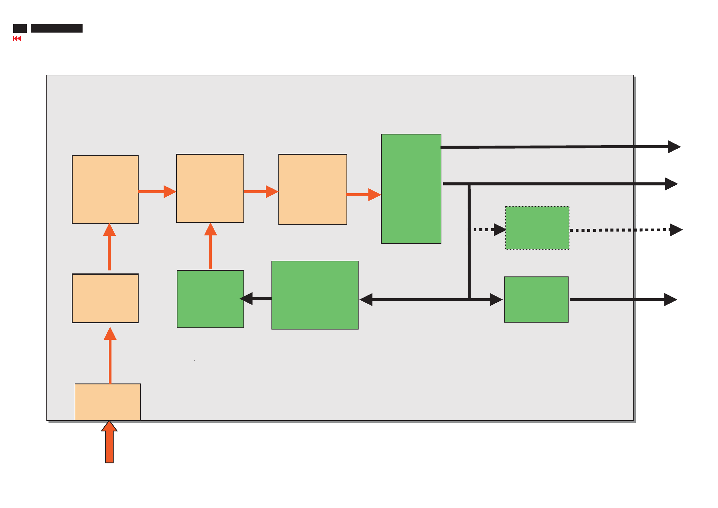
Function Block Diagram
System functional block of HP L2335
HP L2335
Go to cover page
25
Key
&
LED
BD
CVBS
S-Video
D-SUB
DVI-I
AD Converter
AD9888
DDC
DVI RX
THC63DVI161
DDC-D
SW
DDC-A
V. Decoder
SAA7118E
Sil160CT100
30 Pin Connector to panel
TMDS TX
Scaler
PW-172-30V
EEPROM
FlashROM
Component
Input
AC to DC
Power
&
Inverter
BD
AD Converter
AD9883
18V
BL_Ctl, Brightness
3.3V/5V/18V
Panel PWR
Panel Backlight
Page 26
26
Go to cover page
HP L2335
Function Block Diagram
Power board functional block of HP L2335
24V/2.5A to Inverter power
24V/2.5A to Inverter power
18V/0.6 A to Panel power
18V/0.6 A to Panel power
PWM control
PWM control
&
&
MOS Switch
MOS Switch
X’former
X’former
PQ2620
PQ2620
Rectifier &
Rectifier &
filtering
filtering
PFC&pre-
PFC&pre-
Conditioning
Conditioning
5V
5V
5.0V/3.0AScaler
5.0V/3.0AScaler
EMI
EMI
Filter
Filter
AC Inlet
AC Inlet
Opto-
Opto-
coupler
coupler
Feedback &
Feedback &
compensation
compensation
network
network
L4973
L4973
3V3
3V3
L4978
L4978
3.3V/2.0AScaler
3.3V/2.0AScaler
AC Input
90 ~ 264V
Page 27

Schematic diagram(DVI/DSUB)
HP L2335
Go to cover page
27
A
B
C
D
All rights reserved. Reproduction in whole or in parts
is prohibited without the written consent of the copyright
owner.
E
F
G
H
gedeeltelijk, is niet toegestaan dan met schriftelijke
toestemming van de auteursrechthebbende.
Alle rechten voorbehouden. Verveelvuldiging, geheel of
1
2
123456789
+3.3V
A
3231
2201
U74
100K
33p
U80
U81
B
RX5-
RX5+
DVI_CA
NI
3221
100R
3220
10K
C
3206
D
E
DSUBHS
DSUBVS
2K2
3204
F
3203
U103
U102
U101
U99
100R
3205
100R
2K2
DSUB_SDA
DSUB_SCL
15
14
13
12
11
U95
1201
EXCEPT 1201,1202 WERE CHIP COMPONENTS.
12345678
9
47K
3226
NI
0R
3223
3224
100R
DVI_SDA
DVI_SCL
3225
100R
330p
DVI_5V
RXC+
NI
6244
RXC-
NI
6248
NI
6232
DSUBVS DSUBHS
6203
3227
47K
10
DVI_5V
8
VCC
7223
M24C02
5
SDA
VSS
4
+5V_DVI
8
VCC
7224
M24C02
5
SDA
VSS
4
RX3+
NI
6241
RX3-
NI
6245
DSUBR
NI
6214 6212
6204
1
E0
2
E1
E2
SCL
WC_
1
E0
2
E1
E2
SCL
WC_
RX4+
NI
62426237
RX4-
NI
DSUB_SCL DSUB_SDA
6201
47K
3228
3
6
7
6208
47K
3229
3
6
7
NI
6209
6213
3241
10K
LS4148
LS4148
RX5+
RX5-
DSUBBDSUBG
NI
NI
6202
EDID_WC
6243
62476246
NI
A
B
C
D
E
F
12
U74 B1
U75 B3
U76 B2
U77 C2
U78 C2
U79 C2
U80 B1
U81 B1
U82 A5
U83 A5
U84 A5
U85 B5
U86 B6
U87 B6
U88 B7
U89 B7
U90 F2
U91 F2
U92 F2
U93 F2
U94 F2
U95 F1
U96 E2
U97 E2
U98 E2
U99 F1
1201 E2
1202 C2
2201 B1
2202 F4
2203 C3
2204 C4
2205 D2
2206 D2
2207 E5
2209 F2
2215 D2
2216 D3
2217 D5
2218 E3
2219 E3
2222 A4
2223 A4
2224 A5
2225 A5
2226 B7
2227 B7
3201 D2
3202 E2
3203 D1
3204 D1
3205 D1
3206 D1
3207 E2
3208 E2
3209 E3
3210 E3
3211 D3
3212 F3
3213 F3
3214 F4
3215 E3
3216 D5
3217 E5
3218 D3
3219 D3
3220 B1
3221 A1
3222 A7
3223 A7
3224 B7
3225 B7
3226 A7
3227 B7
3228 A9
3229 B9
3230 C7
3231 A1
3232 C3
3233 C3
3234 C3
3235 C3
3236 C3
3237 B3
3238 C3
3239 A3
3240 A3
3241 A9
3242 A3
3243 B3
3252 A3
3253 B3
5212 F3
5213 F3
5214 F3
5215 D3
5220 B3
5221 B3
5222 C3
6201 F9
6202 F9
6203 F7
6204 F8
6205 E4
6206 E5
6207 E5
6208 B9
6209 B9
6212 E9
6213 E9
6214 E8
6215 D3
6216 C5
6217 A4
6218 A4
6219 A5
6220 A5
6230 E6
6231 E7
6232 E7
6233 F5
6234 F5
6235 D5
6236 D6
6237 D7
6238 D5
6239 D6
6240 D7
6241 D8
6242 D9
6243 D9
6244 D7
6245 D8
6246 D9
6247 D9
6248 D7
6251 F6
6252 F7
7222 A6
7223 A8
7224 B8
7225 D4
IXXX D4
U100 A2
U101 F1
U102 E1
U103 E1
U104 D2
U105 E2
U106 E5
NI
NI
5220
100MHZ
5221
100MHZ
5222
100MHZ
5215
3210
10K
4
3239
100R
3240 100R
3252
100R
3242
100R
100R3243
100R
3253
NI
3237 100R
2K2 3232
75R 3233
2216
NI
0R
3211
DSUB_SDA_ROM
DSUB_SCL_ROM
3215
NI
0R
5212
100MHZ
100MHZ5213
5214
100MHZ
323475R
6215
BAT54
100n
75R 3235
3236
2K2
3218
10K
2218
33p
3212
75R
RXCRXC+
RX0+
RX0-
RX1RX1+
RX2RX2+
RX3RX4RX3+
RX4+
2203
330p
100R
3238
3219
10K
2219
33p
3213
75R
5 11
2204
33p
5
DSUB_CA
DSUB_B
DSUB_G
DSUB_R
3214
75R
DVI_A_HS
DVI_A_VS
DVI_A_VS
DVI_A_B
DVI_A_R
DVI_A_G
DVI_A_HS
IXXX
SDA
VSS
6217 BAT54
6218 BAT54
2222
2223
10p
10p
DSUB_5V
8
E0
VCC
E1
7225
E2
M24C02
SCL
4
WC_
+5V
+5V_ESD
2202
220n
+5V
1
2
3
6
7
6205
LS4148
6216
2217
DVIHS
6233
BAV99
6
222410u
BAT54
100n
6206
6219
6220
2225220n
+3.3V
10K
3216
LS4148
BZX84-C5V1
6207
2207
BAT54
BAT54
RX0+
NI
RX0-
NI
U106
220n
NINI
DVIVS
U84
U85
6235
BAV99
6238
BAV99
EDID_WC
3217
6234
U82
U83
0R
+5V_ESD
7
DVI_5V
+5V
+5V_DVI
7222
74LV4053PWT
1
2Y1
2
2Y0
3
3Y1
4
3Z
5
3Y0
6
E
7
VEE
8
GND
VCC
1Y1
1Y0
RX1+
NI
6236
RX1-
NI
6239
+3.3V
DVI_R DVI_G DVI_B
NI
6230
BAV99
DVI_SCL DVI_SDA
6251
3
NI
31
9
11
12
13
15
C3
C4
32
10
14
16
C1
25
29
C5
26
C2
DSUB_HS
DSUB_VS
2205
3201
3202
5
U97
U98
4
3
2
1
1
2
3
4
5
6
7
8
1202
74320-9054
330p
100R
100R
NI
3207
0R
3208
U94
U92
U91
U93
U90
U104
U105
DVI_B
DVI_R
DVI_G
0R
17
18
19
20
21
22
23
24
27
30
C6
28
220633p
17
10
9
8
7
6
16
U100
DVI_5V
DVI_SCL
DVI_SDA
DVIVS
DSUB_SDA1
DSUB_SCL1
U76
U77
U78
U79
2215
U96
2209
NI
NI
U75
DVIHS
100MHZ
100n
+3.3V
3209 100K
DSUBB
DSUBG
DSUBR
100n
+5V_DVI
2Z
1Z
S1
S2
S3
8
NI
0R
U87
U86
RX2+
RX2-
NI
NI
6240
NI
6231
6252
U88
U89
330p
3230
3222
2227
2226
47K
16
15
14
13
12
11
10
9
13
A
B
C
D
E
F
G
H
II
9
CHN SETNAME WUH3 ( HPQ-230W Hanel )
TYT12-
CLASS_NO
1
--------
DVI / DSUB
J
1
SCALER BOARD
SB: 58421 x2
PB: 58431
2 9
0R
Ref Des Reserved
3207 232270296001
3211 232270296001
232270461001
0R
0R
3215 232270296001
3221
100R
0R
232270296001
3222
3223 232270296001
0R
100R
3239 232270461001
4
100R
100R
3240 232270461001
3242 232270461001
3243 232270461001
100R
100R
3252 232270461001
100R
933215370215
3253 232270461001
6212 933215370215
6213
6214 933215370215
5
933215370215
933215370215
BAV993933215370215
6233 933215370215
6230
6231
6232
BAV99
BAV99
6234 933215370215
6235 933215370215
933215370215
BAV99
6238 933215370215
6239 933215370215
6236 933215370215
6237
6
933215370215
6240 933215370215
6241 933215370215
6242 933215370215
6243
9332153702156244
933215370215
6245 933215370215
6246
933215370215
933215370215
6247
6248
7
2003-10-24 3
David Chiang/Edward Chang
NAME
8
IJ6B2W/76
SUPERS.
******** 2003-10-24
CHECKMGr DATE
3138 158 5732
11 1
C
KONINKLIJKE PHILIPS ELECTRONICS N.V. 2000
10 12
11
13010 ***
13
J
A3
Page 28

28
HP L2335
Go to cover page
A
B
C
D
All rights reserved. Reproduction in whole or in parts
is prohibited without the written consent of the copyright
owner.
E
F
gedeeltelijk, is niet toegestaan dan met schriftelijke
toestemming van de auteursrechthebbende.
Alle rechten voorbehouden. Verveelvuldiging, geheel of
G
H
Schematic diagram(ADC)
1
1
A
SCALER BOARD
SB: 58421 x2
PB: 58431
B
C
D
DSUB_HS
DSUB_VS
E
DVI_A_HS
DVI_A_VS
TMDS_VS
TMDS_HS
F
G
H
I
A_DSW
J
1
12345678910
234567891011
7241
74LVC14APW-T
I007
1
I008
3
I009
5
I010
9
I011
11
I012
13
+3.3V
3279
ADC5V
ADC5V
+3.3V
14
VCC
GND
7
_TMDS_HS
10K
7220
MUN2211J
_TMDS_VS
2
2254
LM2937IMP-3.3
2257
100n
2241
2
I013
4
I014
6
I016
8
I017
10
I018
12
I026
7221-A
74LVC126AD
I057
2
7257
2
1
5
4
7254
LM3480IM3-3.3
Vin2Vout
100n
1
Vi3Vo
100n
3293
0R
3294
0R
3295
0R
3296
0R
3277
0R
3278
0R
14
7
14
7
74LVC126AD
8
100n2263
2264 100n
DVDD
I005I004
102
112
OVDD7
GND1867GND19
GND2078GND2188GND2299GND23
68
CHN SETNAME WUH3 ( HPQ-230W Hanel )
TYT12-
CLASS_NO
2003-10-24 3
David Chiang/Edawrd Chang
NAME
100n2266
2265 100n
PVDD
I006
52
47
122
ROUTA0
PVDD248PVDD3
PVDD1
OVDD8
100
ROUTA1
ROUTA2
ROUTA3
ROUTA4
ROUTA5
ROUTA6
ROUTA7
ROUTB0
ROUTB1
ROUTB2
ROUTB3
ROUTB4
ROUTB5
ROUTB6
ROUTB7
GOUTA0
GOUTA1
GOUTA2
GOUTA3
GOUTA4
GOUTA5
GOUTA6
GOUTA7
GOUTB0
GOUTB1
GOUTB2
GOUTB3
GOUTB4
GOUTB5
GOUTB6
GOUTB7
BOUTA0
BOUTA1
BOUTA2
BOUTA3
BOUTA4
BOUTA5
BOUTA6
BOUTA7
BOUTB0
BOUTB1
BOUTB2
BOUTB3
BOUTB4
BOUTB5
BOUTB6
BOUTB7
DATACK
DATACKB
VSOUT
SOGOUT
GND24
HSOUT
GND25
GND26
GND27
GND28
101
111
121
128
CHECKMGr DATE
8
AHSOUT
AVSOUT
A_DSW
10u
2256
10u
2259
SDA
SCL
GHSFOUT
GBLKSPL
GCOAST
_DVI_A_HS
_DVI_A_VS
DVI_A_R
DVI_A_G
DVI_A_B
_DSUB_HS
_DSUB_VS
DSUB_R
DSUB_G
DSUB_B
I060
I061
I063
4
PVDD
DVDD
I074
I075
DVDD
ADC5V
PVDD
2289 100n
3262 100R
3263 100R
3264 10K
I073
3260 0R
3265 10K
I072
I071
I070
0R
I069
0R
I068
0R
I067
0R
I066
0R
I065
0R
9
14
7221-C
74LVC126AD
10
7
12
14
7
13
74LVC126AD
4
8
11
7221-D
3267
3268
3269
3270
3271
3272
39n2285
2286 3n9
100n2287
100n2288
10K3266
5
7251
LM2937IMP-3.3
2251
100n
3261
I085
2290 47n
2291 47n
2293 47n
47n2294
47n2295
2296 1n
47n2297
I058
I059
5
Vi1Vo
3K3
I081
I083
I080
I078
I079
I077
I076
1n2292
GHS
GVS
GND
6
4
2
50
2
9
24
31
32
33
29
30
53
54
45
44
5
13
12
20
43
42
8
17
16
23
3
I003
2252
FILT
REF_BYPASS
RMIDSCV
BMIDSCV
SDA
SCL
A0
CKINV
CLAMP
COAST
CKEXT
HSYNC0
VSYNC0
RAIN0
GAIN0
SOGIN0
BAIN0
HSYNC1
VSYNC1
RAIN1
GAIN1
SOGIN1
BAIN1
5251
100MHZ
47u
2253
1
AVDD1
AVDD26AVDD37AVDD410AVDD514AVDD618AVDD721AVDD825AVDD9
GND1
GND2
GND315GND419GND5
3
4
11
22
6
AVDD
10u
AVDD
GND627GND728GND835GND9
GND1040GND1141GND1246GND1349GND1451GND1555GND1665GND17
36
7
AVDD
100n2261
2262 100n
56
38
39
26
OVDD1
AVDD1034AVDD1137AVDD12
AVDD13
7261
AD9888KS-205
7
OVDD269OVDD379OVDD489OVDD598OVDD6
66
3 12
5254
I001
1
2243
2245
2247
2249
2244
I056
2246
2255
I002
2258
_DSUB_HS
33p
_DSUB_VS
33p
_DVI_A_HS
33p
_DVI_A_VS
33p
_TMDS_VS
33p
_TMDS_HS
33p
+3.3V
2242
100MHZ
47u
5257
100MHZ
47u
100n
GND
GND
3
6
7221-B
3
4
2
I027
I028
I029
I030
3
9
2267 100n
100n2268
120
119
118
117
116
115
114
113
110
109
108
107
106
105
104
103
97
96
95
94
93
92
91
90
87
86
85
84
83
82
81
80
77
76
75
74
73
72
71
70
64
63
62
61
60
59
58
57
123
124
127
126
125
100n2269
AGRE0
AGRE1
AGRE2
AGRE3
AGRE4
AGRE5
AGRE6
AGRE7
AGRO0
AGRO1
AGRO2
AGRO3
AGRO4
AGRO5
AGRO6
AGRO7
AGGE0
AGGE1
AGGE2
AGGE3
AGGE4
AGGE5
AGGE6
AGGE7
AGGO0
AGGO1
AGGO2
AGGO3
AGGO4
AGGO5
AGGO6
AGGO7
AGBE0
AGBE1
AGBE2
AGBE3
AGBE4
AGBE5
AGBE6
AGBE7
AGBO0
AGBO1
AGBO2
AGBO3
AGBO4
AGBO5
AGBO6
AGBO7
I182
I183
I184
I185
100n2270
3273 47R
3275 47R
ADC
IJ6B2W/76
SUPERS.
******** 92-07-25
9
2271 100n
10
DVDD
100n2272
2274 100n
2273 100n
AGRE0
I086
1
I087
AGRE1
2
AGRE2
AGRE3
AGRO0
AGRO1
AGRO2
AGRO3
AGGE0
AGGE1
AGGE2
AGGE3
AGGO0
AGGO1
AGGO2
AGGO3
AGBE0
AGBE1
AGBE2
AGBE3
AGBO0
AGBO1
AGBO2
AGBO3
47R3274
47R3276
NI
2298
3281
I088
3
I089
45
1
I102
2
I103
3283
3
I105
45
I118
1
I119
2
3285
I120
3
I121
45
I134
1
I135
2
3287
I136
3
I137
4
I150
1
I151
2
3289
3
45
I166
1
I167
2
3291
I168
3
I169
45
I186
I189
2p2
33p
2299
11 13
47R
47R
47R
47R
47R
47R
2276 100n
8
7
6
8
7
6
8
7
6
8
7
6
5
8
7
6
8
7
6
I090
I091
I092
I093
I122
I123
I124
I125
I154
I155
I156
I157
100n2277
GRE0
GRE1
GRE2
GRE3
GRO0
GRO1
GRO2
GRO3
GGE0
GGE1
GGE2
GGE3
GGO0
GGO1
GGO2
GGO3
GBE0
GBE1
GBE2
GBE3
GBO0
GBO1
GBO2
GBO3
100n2278
2279 100n
AGRE4
AGRE5
AGRE6
AGRE7
AGRO4
AGRO5
AGRO6
AGRO7
AGGE4
AGGE5
AGGE6
AGGE7
AGGO4
AGGO5
AGGO6
AGGO7
AGBE4
AGBE5
AGBE6
AGBE7
AGBO4
AGBO5
AGBO6
AGBO7
Ref Des
2243
2244 223886775339
2245
2246
2247
2249 223886775339
2298
2299
GCLK
AVSOUT
AHSOUT
GFBK
NI
100n2275
R
R
R
R
R
R
R
R
R
R
R
R
R
R
R
R
R
R
R
R
R
R
R
R
3138 158 5732
11 2
C
KONINKLIJKE PHILIPS ELECTRONICS N.V. 2000
10
11
12
PVDD
100n2280
100n
2281
I094
1
I095
2
3282
I096
3
I097
45
I110
1
I111
2
3284
I112
3
I113
45
I126
1
I127
2
3286
I128
3
I129
45
I142
1
I143
2
3288
I144
3
I145
45
I158
1
I159
2
3290
I160
3
I161
45
I174
1
I175
2
3292
I176
3
I177
45
NI
223886775339
33p
33p
223886775339
33p
223886775339
33p
223886775339
33p
33p
223886775228
2p2
223886775339
33p
13010 *** A3
12
100n2282
2283 100n
I098
GRE4
8
R
I099
GRE5
7
R
47R
I100
GRE6
6
R
I101
R
R
R
47R
R
R
R
R
47R
R
R
R
R
47R
R
R
R
R
47R
R
R
R
R
47R
R
R
GRE7
GRO4
8
GRO5
7
GRO6
6
GRO7
I130
GGE4
8
I131
GGE5
7
I132
GGE6
6
I133
GGE7
GGO4
8
GGO5
7
GGO6
6
GGO7
I162
GBE4
8
I163
GBE5
7
I164
GBE6
6
I165
GBE7
GBO4
8
GBO5
7
GBO6
6
GBO7
1
--------
13
11 12
100n2284
A
B
C
D
E
F
G
H
I
J
A
B
C
D
E
F
G
H
2241 C2
2242 G3
2243 C3
2244 E3
2245 D3
2246 F3
2247 D3
2249 E3
2251 A5
2252 A6
2253 A6
2254 A3
2255 A3
2256 A4
2257 B3
2258 B3
2259 B4
2261 A7
2262 A7
2263 A7
2264 A7
2265 A8
2266 A8
2267 A8
2268 A8
2269 A8
2270 A9
2271 A9
2272 A9
2273 A9
2274 A10
2275 A10
2276 A10
2277 A10
2278 A10
2279 A11
2280 A11
2281 A11
2282 A12
2283 A12
2284 A12
2285 C5
2286 C5
2287 C5
2288 C5
2289 C5
2290 E5
2291 E5
2292 E5
2293 E5
2294 F5
2295 F5
2296 F5
2297 F5
2298 G9
2299 G9
3260 D5
3261 C5
3262 D5
3263 D5
3264 D5
3265 D5
3266 D5
3267 E5
3268 E5
3269 E5
3270 F5
3271 F5
3272 F5
3273 F9
3274 G9
3275 G9
3276 G9
3277 E3
3278 F3
3279 G2
3281 B10
3282 B11
3283 C10
3284 C11
3285 C10
3286 C11
3287 D10
3288 D11
3289 E10
3290 E11
3291 E10
3292 E11
3293 C3
3294 D3
3295 D3
3296 E3
5251 A6
5254 A4
5257 B4
7220 G2
7221-A G3
7221-B H3
7221-C G5
7221-D H5
7241 C2
7251 A5
7254 A3
7257 B3
7261 E7
I001 A3
I002 B3
I003 A6
I004 B6
I005 B7
I006 B8
I007 D2
I008 D2
I009 D2
I010 D2
I011 D2
I012 E2
I013 D3
I014 D3
I016 D3
I017 D3
I018 E3
I026 E3
I027 C3
I028 D3
I029 D3
I030 E3
I056 F3
I057 G2
I058 G5
I059 H5
I060 G4
I061 H4
I063 H4
I065 F4
I066 F4
I067 F4
I068 E4
I069 E4
I070 E4
I071 D4
I072 D4
I073 D4
I074 D4
I075 D4
I076 D5
I077 D5
I078 D5
I079 D5
I080 D5
I081 C5
I083 C5
I085 C5
I086 B9
I087 B9
I088 B9
I089 B9
I090 B10
I091 B10
I092 B10
I093 B10
I094 B11
I095 B1
I096 B11
I097 B11
I098 B12
I099 B12
I100 B12
I101 B12
I102 C9
I103 C9
I105 C9
I110 C11
I111 C11
I112 C11
I113 C11
I118 C9
I119 C9
I120 D9
I121 D9
I122 C1
I123 C10
I124 D10
I125 D10
I126 C11
I127 C11
I128 D11
I129 D11
I130 C12
I131 C12
I132 D12
I133 D12
I134 D9
I135 D9
I136 D9
I137 D9
I142 D11
I143 D11
I144 D11
I145 D11
I150 E9
I151 E9
I154 E10
I155 E10
I156 E10
I157 E10
I158 E11
I159 E11
I160 E11
I161 E11
I162 E12
I163 E12
I164 E12
I165 E12
I166 E9
I167 E9
I168 E9
I169 F9
I174 E11
I175 E11
I176 E11
I177 F11
I182 F8
I183 G8
I184 G8
I185 G8
I186 F9
I189 G9
1
0
Page 29
Schematic diagram(TMSD RX)
HP L2335
Go to cover page
29
1
3
4
5
62
7
12345
8
6
9
10
11
789
A
10u
10u
10u
OVCC1
10u
CVCC1
2319 470p
AVCC1
OVCC1
CVCC1
AVCC1
TMDSRXPD
2309
100n
PVCC1
3308
3309
470p2320
I206
10K
0R05
3304
3306
3307
SCDT2
NI
2321 470p
3301
SCDT1
RX2RX2+
RX1RX1+
RX0RX0+
RXC+
RXC-
3303
0R
NI
510R
OVCC1
3302
10K
10K3305
10K
10K
3327
I195
I196
I197
I198
I200
I201
I202
I203
I204
I205
0R05
I207
NI
I210
I211
I212
CVCC1
I192
6
38
VCC167VCC3
TOUT
GND168GND3
5
39
PVCC1
TEST
I193
97
PVCC
PGND
98
2322
100n
SCDT
ODCK
VSYNC
HSYNC
B10
B11
B12
B13
B14
B15
B16
B17
G10
G11
G12
G13
G14
G15
G16
G17
R10
R11
R12
R13
R14
R15
R16
R17
B20
B21
B22
B23
B24
B25
B26
B27
G20
G21
G22
G23
G24
G25
G26
G27
R20
R21
R22
R23
R24
R25
R26
R27
CT1
CT2
CT3
M_DE
I215
47R3310
8
44
46
DE
47
48
10
11
12
13
14
15
16
17
20
21
22
23
24
25
26
27
30
31
32
33
34
35
36
37
49
50
51
52
53
54
55
56
59
60
61
62
63
64
65
66
69
70
71
72
73
74
75
77
40
41
42
I217
I218
I219
I220
I221
I222
I223
I225
I226
I227
I228
I229
I230
I231
I232
I233
I234
I235
I236
I237
I238
I239
I240
I241
I242
I243
I244
I245
I246
I247
I248
I249
I250
I251
I252
I253
I254
I256
I257
I258
I260
I261
I262
I263
I264
3311 47R
47R3312
PGBE0
PGBE1
PGBE2
PGBE3
PGBE4
PGBE5
PGBE6
PGBE7
PGGE0
PGGE1
PGGE2
PGGE3
PGGE4
PGGE5
PGGE6
PGGE7
PGRE0
PGRE1
PGRE2
PGRE3
PGRE4
PGRE5
PGRE6
PGRE7
PGBO0
PGBO1
PGBO2
PGBO3
PGBO4
PGBO5
PGBO6
PGBO7
PGGO0
PGGO1
PGGO2
PGGO3
PGGO4
PGGO5
PGGO6
PGGO7
PGRO0
PGRO1
PGRO2
PGRO3
PGRO4
PGRO5
PGRO6
PGRO7
2323
GFBK
SCDT1
GCLK
I216
GPEN
TMDS_VS
TMDS_HS
NI
2p2
45
PGBE0
PGBE1
PGBE2
PGBE3
PGGE0
PGGE1
PGGE2
PGGE3
PGRE0
PGRE1
PGRE2
PGRE3
PGBO0
PGBO1
PGBO2
PGBO3
PGGO0
PGGO1
PGGO2
PGGO3
PGRO0
PGRO1
PGRO2
PGRO3
R
3
R
3313
2
R
1
R
45
R
3
R
3315
2
R
1
R
45
R
3
R
3317
2
R
1
R
45
R
3
R
3319
2
R
1
R
45
R
3
R
3321
2
R
1
R
45
R
3
R
3323
2
R
1
R
47R
47R
47R
47R
47R
47R
6
7
8
6
7
8
6
7
8
6
7
8
6
7
8
6
7
8
Ref Des Reserved
2323
3302
3306 319802131031
3309
3327 319802190030
GBE0
GBE1
GBE2
GBE3
GGE0
GGE1
GGE2
GGE3
GRE0
GRE1
GRE2
GRE3
GBO0
GBO1
GBO2
GBO3
GGO0
GGO1
GGO2
GGO3
GRO0
GRO1
GRO2
GRO3
223886775228
2p2
319802131030
10K
10K
319802190030
0R05
0R05
4
PGBE4
3
PGBE5
PGBE6
PGBE7
PGGE4
PGGE5
PGGE6
PGGE7
PGRE4
PGRE5
PGRE6
PGRE7
PGBO4
PGBO5
PGBO6
PGBO7
PGGO4
PGGO5
PGGO6
PGGO7
PGRO4
PGRO5
PGRO6
PGRO7
3314
2
1
45
3
3316
2
1
45
3
3318
2
1
45
3
3320
2
1
45
3
3322
2
1
4
3
3324
2
1
5
R
6
R
47R
7
R
8
R
R
6
R
47R
7
R
8
R
R
6
R
47R
7
R
8
R
R
6
R
47R
7
R
8
R
R
6
R
47R
7
R
8
R
5
R
6
R
47R
7
R
8
R
OVCC1
AVCC1
I190
82
AVCC184AVCC288AVCC395AVCC4
96
EXT_RES
9
PDO
81
RX2-
80
RX2+
86
RX1-
85
RX1+
91
RX0-
90
RX0+
93
RXC+
94
RXC-
NI
10K
2
PD
OCK_INV
100
PIXS
4
STAG_OUT
7
RSVD
99
DFO
1
ST
3
AGND183AGND2
79
THC63DV161
AGND389AGND492AGND5
87
I191
18
OVCC129OVCC243OVCC357OVCC478OVCC5
7301
OGND128OGND245OGND358OGND476OGND5
19
3325
0R05
2
OVCC1
470p2315
2314 470p
3
I194
Vo
2302
2316 470p
5301
100MHZ
5302
100MHZ
5303
100MHZ
47u
470p2317
470p2318
2303
2304
2305
AVCC1
A
B
C
B
D D
470p2310
TMDSRX5V
2311 470p
TMDSRX1
LM2937IMP-3.3
2301
100n
7302
1
470p2312
2313 470p
4
Vi
GND
C
All rights reserved. Reproduction in whole or in parts
is prohibited without the written consent of the copyright
owner.
E
D
F
I213
LM3480IM3-3.3
100n
3326
0R05
7303
Vin2Vout
GND
3
2307
47u
5304
100MHZ
2308
I214
1
G
E
TMDSRX2
TMDSRX5V
2306
H
F
gedeeltelijk, is niet toegestaan dan met schriftelijke
Alle rechten voorbehouden. Verveelvuldiging, geheel of
toestemming van de auteursrechthebbende.
I
12345
J
1
SCALER BOARD
SB: 58421 x2
PB: 58431
2
3
4
5
6
7
67
CHN SETNAME WUH3 (HPQ-230W Hanel )
TYT12-
CLASS_NO
TMDS RX MASTER
IJ6B2W/76
2003-10-24 3
David Chiang/Edward Chang
NAME
CHECKMGr DATE
SUPERS.
******** 2003-10-24
9
89
3138 158 5732
11 3
C
KONINKLIJKE PHILIPS ELECTRONICS N.V. 2000
108
11
12
A
B
GBE4
GBE5
GBE6
GBE7
GGE4
GGE5
GGE6
GGE7
GRE4
GRE5
GRE6
GRE7
GBO4
GBO5
GBO6
GBO7
GGO4
GGO5
GGO6
GGO7
GRO4
GRO5
GRO6
GRO7
13010 *** A3
C
D
E
F
12
2301 C1
2302 D2
2303 B3
2304 C3
2305 C3
2306 E1
2307 E2
2308 E3
2309 D3
2310 A1
2311 A1
2312 A1
2313 A1
2314 A2
2315 A2
2316 A2
2317 A2
2318 A3
2319 A3
2320 A3
2321 A3
2322 A6
2323 B7
3301 B4
3302 D4
3303 D4
3304 D3
3305 D3
3306 D3
3307 D3
3308 D3
3309 E3
3310 A6
3311 B6
3312 B6
3313 C7
3314 C9
3315 C7
3316 C9
3317 D7
3318 D9
3319 E7
3320 E9
3321 E7
3322 E9
3323 F7
3324 F9
3325 B1
3326 D1
5301 B2
5302 C2
5303 C2
5304 E2
7301 D5
7302 B1
7303 E1
I190 A4
I191 A5
I192 A5
I193 A5
I194 C2
I195 B4
I196 B4
I197 C4
I198 C4
I200 C4
I201 C4
I202 C4
I203 C4
I204 C4
I205 C4
I206 D3
I207 D4
I210 D4
I211 D4
I212 D4
I213 E1
I214 E2
I215 A7
I216 B7
I217 B6
I218 B6
I219 B6
I220 B6
I221 B6
I222 B6
I223 B6
I225 C6
I226 C6
1
13
13
I227 C6
I228 C6
I229 C6
I230 C6
I231 C6
I232 C6
I233 C6
I234 C6
I235 C6
I236 D6
I237 D6
I238 D6
I239 D6
I240 D6
I241 D6
I242 D6
I243 D6
I244 D6
I245 D6
I246 D6
I247 D6
I248 D6
I249 E6
I250 E6
I251 E6
I252 E6
I253 E6
I254 E6
I256 E6
I257 E6
I258 E6
I260 E6
I261 F6
I262 F6
I263 F6
I264 F6
--------
A
B
C
E
F
G
H
I
J
Page 30
30
HP L2335
Go to cover page
Schematic diagram(TMSD RX SLAVE)
A
B
C
D
All rights reserved. Reproduction in whole or in parts
owner.
is prohibited without the written consent of the copyright
E
F
G
H
gedeeltelijk, is niet toegestaan dan met schriftelijke
Alle rechten voorbehouden. Verveelvuldiging, geheel of
toestemming van de auteursrechthebbende.
A
B
C
D
E
F
AVCC2
2350 470p
TMDSRX5V
TMDSRX5V
21
470p2351
LM2937IMP-3.3
2341
100n
2346
100n
470p2353
2352 470p
7342
1
Vi
7343
LM3480IM3-3.3
Vin2Vout
GND
GND
3
I655
I656
I657
I658
I659
I670
I671
I672
I673
I674
I675
I676
I677
I669
I660
I661
I662
I663
I664
I665
I666
I667
I668
U1
SCDT2
SGBE0
SGBE1
SGBE2
SGBE3
SGBE4
SGBE5
SGBE6
SGBE7
SGGE0
SGGE1
SGGE2
SGGE3
SGGE4
SGGE5
SGGE6
SGGE7
SGRE0
SGRE1
SGRE2
SGRE3
SGRE4
SGRE5
SGRE6
SGRE7
98
10
45
SGBE0
SGBE1
SGBE2
SGBE3
SGBE4
SGBE5
SGBE6
SGBE7
SGGE0
SGGE1
SGGE2
SGGE3
SGGE4
SGGE5
SGGE6
SGGE7
SGRE0
SGRE1
SGRE2
SGRE3
SGRE4
SGRE5
SGRE6
SGRE7
R
3
R
3349
2
R
1
R
45
R
3
R
3350
2
R
1
R
45
R
3
R
3351
2
R
1
R
45
R
3
R
3352
2
R
1
R
45
R
3
R
3353
2
R
1
R
45
R
3
R
3354
2
R
1
R
47R
47R
47R
47R
47R
47R
11 12 13
GBO0
6
GBO1
7
GBO2
8
GBO3
GBO4
6
GBO5
7
GBO6
8
GBO7
GGO0
6
GGO1
7
GGO2
8
GGO3
GGO4
6
GGO5
7
GGO6
8
GGO7
GRO0
6
GRO1
7
GRO2
8
GRO3
GRO4
6
GRO5
7
GRO6
8
GRO7
A
B
C
D
E
F
2341 E1
2342 E2
2343 C3
2344 D3
2345 E3
2346 F1
2347 F2
2348 F3
2349 D4
2350 C1
2351 C1
2352 C1
2353 C1
2354 C2
2355 C2
2356 C2
2357 C2
2358 C3
2359 C3
2360 C3
2361 C3
2362 A6
3341 C4
3342 C4
3343 D4
3344 D4
3345 D4
3346 D4
3347 D4
3348 A4
3349 D8
3350 B8
3351 E8
3352 C8
3353 E8
3354 C8
5341 C2
5342 D2
5343 D2
5344 E2
7341 C5
7342 D1
7343 E1
I640 D2
I641 C3
I642 D3
I643 D3
I644 E3
I645 B4
I646 B4
I647 B4
I648 B4
I649 C4
I650 C4
I653 C4
I654 D4
I655 B7
I656 B7
I657 B7
I658 B7
I659 B7
I660 C7
I661 C7
I662 C7
I663 C7
I664 C7
I665 C7
I666 C7
I667 C7
I668 C7
I669 B7
I669 C7
I670 B7
I671 B7
I672 B7
I673 B7
I674 B7
I675 B7
I676 C7
I677 C7
A
B
C
D
E
F
G
H
6543
2341
AVCC2
OVCC2
3
TMDSRX1
TMDSRX2
2355 470p
I640
470p2356
2342
2347
2357 470p
5341
100MHZ
5342
100MHZ
5343
100MHZ
47u
5344
100MHZ
47u
470p2354
4
Vo
2
1
2358 470p
2343
2344
2345
2348
CVCC2
470p2359
I641
I642
I643
I644
10u
10u
10u
10u
2360 470p
CVCC2
AVCC2
PVCC2
OVCC2
470p2361
OVCC2
TMDSRXPD
2349
AVCC2
100n
3346
3347
3348
SCDT2
RX5RX5+
RX4RX4+
RX3RX3+
RXC+
RXC-
3342
0R05
3344
10K
3345
I654
0R
390R
I645
I646
I647
I648
I649
I650
OVCC2
3341
10K
3343
I653
10K
10K
10K
M_DE
100
96
9
81
80
86
85
91
90
93
94
2
4
7
99
1
3
EXT_RES
PDO
RX2RX2+
RX1RX1+
RX0RX0+
RXC+
RXC-
PD
OCK_INV
PIXS
STAG_OUT
RSVD
DFO
ST
AGND179AGND283AGND387AGND489AGND5
7
56789
PVCC2
CVCC2
78
OVCC118OVCC229OVCC343OVCC457OVCC5
7341
SiI163B
OGND119OGND228OGND345OGND458OGND5
76
67
VCC16VCC238VCC3
GND15GND239GND3
68
97
PVCC
PGND
98
2362
100n
SCDT
ODCK
VSYNC
HSYNC
QE0
QE1
QE2
QE3
QE4
QE5
QE6
QE7
QE8
QE9
QE10
QE11
QE12
QE13
QE14
QE15
QE16
QE17
QE18
QE19
QE20
QE21
QE22
QE23
QO0
QO1
QO2
QO3
QO4
QO5
QO6
QO7
QO8
QO9
QO10
QO11
QO12
QO13
QO14
QO15
QO16
QO17
QO18
QO19
QO20
QO21
QO22
QO23
CT1
CT2
CT3
8
44
46
DE
47
48
10
11
12
13
14
15
16
17
20
21
22
23
24
25
26
27
30
31
32
33
34
35
36
37
49
50
51
52
53
54
55
56
59
60
61
62
63
64
65
66
69
70
71
72
73
74
75
77
40
41
42
82
AVCC284AVCC388AVCC4
AVCC1
OVCC2
95
92
I
123
45678
TYT12-
CLASS_NO
WUH3 ( HPQ-230W Hanel )SETNAMECHN
9
1
--------
I
TMDS RX SLAVE
J
1
SCALER BOARD
SB: 58421 x2
PB: 58431
2 13121110
34 5
6
7
NAME
32003-10-24
David Chiang/Edward Chang
89
IJ6B2W/76
SUPERS.
DATECHECK
2003-10-24
3138 158 5732
C
KONINKLIJKE PHILIPS ELECTRONICS N.V. 2000
411
J
A3130
Page 31

Schematic diagram(SCALER Pw172)
HP L2335
Go to cover page
31
G
A
B
C
D
E
F
H
1
A
B
C
D
All rights reserved. Reproduction in whole or in parts
is prohibited without the written consent of the copyright
owner.
E
F
G
H
gedeeltelijk, is niet toegestaan dan met schriftelijke
Alle rechten voorbehouden. Verveelvuldiging, geheel of
toestemming van de auteursrechthebbende.
I
J
1 13
SCALER BD
SB: 58421 x2
PB: 58431
3V3
4K7 3401
340210K
NI
1
2345
5
2419100n
2421100n
100n 2420
D9
D10
D11
D12
U8
D10V7D11W6D12Y6D13
VB0L2VB1L1VB2L3VB3L4VB4M3VB5M1VB6
VUV0
VUV1
VUV2
VUV3
VUV4
VUV5
5
100n 2422
D13
VUV6
D14
V6
N1
VUV7
2423100n
D15
D14U7D15
VB7
M2
34114K7
0R 3412
U14
U12
P17
N18
N17
N13
N12
N11
N10
M13
M12
M11
M10
L18
L13
L12
L11
L10
K13
K12
K11
K10
J13
J12
J11
J10
H13
H12
H11
H10
G17
D15
D13
D12
D11
2
3V3
MODE3
V14
DNC2
P2
I277
B20
C19
DNC0
DNC1
MODE1
MODE2
T5
N4
I285
I284
5406
2406
A_DSW
MODE0
U16
I286
2
+2.5V
100MHZ
47u
DVI_CA
T17
PORTC0
PORTC1
CPUTDO
TDO
3407
3V3
I291
2V5
SCDT1
DSUB_CA
TMDSRXPW
V16
Y16
W16
PORTC2
PORTC3
CPUTCK
CPUTDI
Y2
N3
M4
I289
TDI
TCK
TMS
4K7
ADCPW
TMDSRXPD
V17
U17
PORTC4
PORTC5
CPU_TMS
ADR24B
P1
U15
+3.3V_S
5405
I287
100MHZ
47u
2405
VSS58
Y7
VSS57
VSS56
VSS55
R5
VSS54
VSS53
VSS52
VSS51
VSS50
VSS49
VSS48
VSS47
N9
VSS46
N8
VSS45
VSS44
VSS43
VSS42
VSS41
M9
VSS40
M8
VSS39
VSS38
VSS37
VSS36
VSS35
VSS34
L9
VSS33
L8
VSS32
VSS31
VSS30
VSS29
VSS28
K9
VSS27
K8
VSS26
K4
VSS25
VSS24
VSS23
VSS22
VSS21
J9
VSS20
J8
VSS19
VSS18
VSS17
VSS16
VSS15
H9
VSS14
H8
VSS13
H4
VSS12
G4
VSS11
VSS10
VSS9
VSS8
VSS7
VSS6
D9
VSS5
D8
VSS4
D5
VSS3
D4
VSS2
B3
VSS1
B2
VSS0
A1
34314K7
4K7 3421
342210K
10K 3432
NI
NI
3V3
2411100n
100n 2410
DC_KEY
SLEEPLED
TMDSTXPW
POWERLED
Y17
R17
W18
W17
PORTB0
PORTB1
PORTC6
PORTC7
NMI
EXTINT
U10
W10
NMI
CS0
EXTINT
3
100n 2412
EEWR
LCDPW
V18
Y18
PORTB2
PORTB3
CS0V4CS1
Y4
1
3
2413100n
VIDEOPW
BL_ENABLE
Y19
U18
PORTB4
PORTB5
RAMOE
RAMWE
Y5
W5
ROMWE
4401
2
34053K3
SDA
PWR_SAVING
T18
W19
PORTB6
PORTB7
ROMOE
ROMWE
V5
W4
BHEN
ROMOE
R
3K3 3406
SCL
ISP_SW
EDID_WC
VIDEO_CE
I280
V13
Y13
Y14
W13
PORTA0
PORTA1
PORTA2
PORTA3
WR
RDW3RESET
BHEN
Y3
W12
WR
RD
2401
4
2415100n
100n 2414
BL_BRI
VOLUME
3409
10K
10K3408
D0D1D2D3D4D5D6D7D8
Y15
V15
W14
W15
D0
PORTA4
PORTA5
PORTA6
PORTA7
XI
XO
MCKEXT
E5
C5
Y11
I281
I282
RESET
MCKEXT
3413
1M
1401
14M31818HZ
18p
4
2417100n
100n 2416
100n 2418
2409100n
V10D1Y10
D2Y9D3W9D4V9D5Y8D6W8D7V8D8W7D9
RXD
TXD
IRRCVRI
IRRCVRO
A3
Y12
V12
V11
W11
I283
TXD
RXD
18p
2402
100n2408
100n 2424
A0A1A2A3A4A5A6A7A8
U6
A0U4A1
VG0J4VG1H1VG2
VY0
VY1
3433
3434
47R
47R
Ref Des
3402
3411
3422
3432
12345
2425100n
100n 2426
T4
A2V3A3U3A4Y1A5W2A6T3A7
VG3J2VG4J1VG5K3VG6K2VG7
J3
VY2
VY3
VY4
VY5
3436
3435
3437
3438
47R
47R
47R
47R
6789
2427100n
100n 2428
A9
V2
A8U2A9
VR0E2VR1F1VR2F2VR3G3VR4G2VR5H3VR6H2VR7
K1
VR0
VY6
VY7
3439
3440
47R
47R
NI
319802131030
10K
319802134720
4K7
319802131030
10K
319802131030
10K
6
1V5
2429
2431100n
100n 2430
100n
A10
A11
W1
A10R4A11V1A12P4A13R3A14T2A15U1A16T1A17R2A18R1A19
A12
A13
A14
A15
A16
A17
100n 2432
A18
PW172-30V
G1
VR1
VR2
VR3
VR4
VR5
VR6
VR7
3441
47R
7
2433100n
A19
P3
7401
FIELD
D1
VFIELD
3442
3443
47R
47R
100n 2434
DEN
DCKEXT
I288
D6
DCKEXT
VVS
VHSF3VPEN
E3
VVS
VHS
VPEN
3444
3445
47R
47R
7
8
I293
2439100n
2437100n
GBO1
GBO1
DBOI0
I039
E17
GBO2
DBOI1
I082
E20
DBO0
GBO2
C17
GBO3
100n 2438
DBOI2
I084
E19
DBO1
GBO3
B19
GBO4
DBOI3
I104
E18
DBO2
GBO4
E16
GBO5
DBOI4
I106
F17
DBO3
GBO5
C16
GBO6
DBO4
GBO6
DBOI5
I107
D20
DBO5
GBO7
C15
GBO7
100n 2440
DBOI6
I108
I109
D19
D16
DBO6
D14
DBOI7
D17
DBO7
GGO0
C13
GGO0
GGO1
DGOI0
I114
GGO1
B15
GGO2
100n 2442
DGOI1
I115
H18
DGO0
GGO2
A14
GGO3
EXCEPT 4401 WERE CHIP COMPONENTS.
TYT12-
CLASS_NO
DEN
3446
47R
2435100n
DHSI
I278
N19
N2
VCLK
DVSI
I279
D18
DHS
VCLK
E1
3447
47R
100n 2436
DCLK
I290
C20
DVS
GBO0
3448
47R
J17
DCLK
GBO0
C18
SCALER PW172
32003-10-24
NAME
David Chiang/Edward Chang
8
9
2445100n
2443100n
100n 2444
DGOI7
DGOI6
DGOI5
DGOI4
DGOI2
DGOI3
I117
I116
I141
I139
I140
I138
F20
F19
G20
DGO2
GGO4
A13
GGO5
G19
DGO3
GGO5
C12
GGO6
G18
DGO4
GGO6
B13
GGO7
F18
DGO5
DGO6
DGO7
GRO0A6GRO1C7GRO2B6GRO3A5GRO4D7GRO5B5GRO6C6GRO7
GGO7
A12
GRO0
H17
DGO1
GGO3
B14
GGO4
IJ6B2W/76
SUPERS.
DATEMGr CHECK
9
GRO1
100n 2446
DROI0
I146
K19
DRO0
GRO2
2447100n
DROI1
DROI2
I148
I147
K20
DRO1
GRO3
GRO4
DROI3
I149
K18
DRO2
GRO5
2003-10-24********
100n 2448
DROI4
I152
J20
DRO3
GRO6
WUH3 ( HPQ-230W Hanel )SETNAMECHN
DROI5
I153
J18
DRO4
GRO7
2449100n
DROI6
I170
J19
DRO5
A4
DROI7
I171
H20
DRO6
GBE0
100n 2450
H19
DRO7
GBE0
B18
GBE1
DBEI0
I172
GBE1
A20
GBE2
106
DBEI1
I173
M17
DBE0
GBE2
B17
GBE3
10
6789
DBEI2
I178
N20
DBE1
GBE3
A19
GBE4
100n 2452
DBEI3
I179
M20
DBE2
GBE4
B16
GBE5
DBEI4
I180
L17
DBE3
GBE5
A17
GBE6
2453100n
DBEI5
I181
M19
DBE4
GBE6
A16
GBE7
DBEI6
I187
K17
DBE5
GBE7
A15
100n 2454
DBEI7
I188
L19
DBE6
GGE0
10 11 12
DREI2
I270
Y20
DRE2
GRE4
DREI3
I271
R16
C2
GRE5
DREI6
DREI5
DREI4
I272
I273
I274
U19
R18
W20
DRE3
DRE4
DRE5
GRE5C1GRE6D3GRE7
D2
GRE6
GRE7
12
2V5
2463100n
DREI7
I275
V20
DRE6
GFBK
U20
DRE7
GFBK
A11
GSOG
2465100n
100n 2464
GCOAST
GBLKSPL
GHSFOUT
C9
C14
GBLKSPL
GHSFOUT
GVS
GHS
A9
B10
C10
GVS
GHS
GPEN
100n 2466
A18
D10
VDD42
GREF
VDD41
GCOAST
VDD40
VDD39
VDD38
VDD37
VDD36
VDD35
VDD34
VDD33
VDD32
VDD31
VDD30
VDD29
VDD28
VDD27
VDD26
VDD25
VDD24
VDD23
VDD22
VDD21
VDD20
VDD19
VDD18
VDD17
VDD16
VDD15
VDD14
VDD13
VDD12
VDD11
VDD10
VDD9
VDD8
VDD7
VDD6
VDD5
VDD4
VDD3
VDD2
VDD1
VDD0
VCC18
VCC17
VCC16
VCC15
VCC14
VCC13
VCC12
VCC11
VCC10
VCC9
VDD 3.3 VDD1.5 VDD2.5
VCC8
VCC7
VCC6
VCC5
VCC4
VCC3
VCC2
VCC1
VCC0
GPEN
GCLK
B9
A10
GCLK
L20
DBE7
GGE0
C11
GGE1
2455100n
DGEI0
I324
GGE1
B12
GGE2
11
100n 2456
100n 2457
DGEI1
DGEI4
DGEI2
DGEI3
I345
I343
I344
I325
T19
T20
R20
R19
DGE3
DGE0
DGE1
DGE2
GGE2
GGE3A8GGE4B8GGE5C8GGE6A7GGE7
B11
GGE3
GGE4
GGE5
GGE6
DGEI5
I265
M18
DGE4
GGE7
2458100n
DGEI6
I266
P18
DGE5
B7
DREI1
DREI0
DGEI7
I267
I269
I268
V19
P19
P20
DRE0
DGE6
DGE7
GRE0E4GRE1C3GRE2B1GRE3F4GRE4
GRE0
GRE1
GRE2
GRE3
DRE1
3138 158 5732
511
C
KONINKLIJKE PHILIPS ELECTRONICS N.V. 2000
11
12
10 11 12
2467100n
3404
0R
U13
U11
T16
T15
T14
T13
T12
T11
T10
R15
R14
R13
P16
P15
N16
N15
K16
H16
F16
E15
E14
E13
E12
E11
E10
M16
L16
J16
G16
G15
F15
F14
1401 H4
2401 H4
2402 H4
2405 A2
2406 A2
2408 B4
2409 B4
2410 A3
2411 A3
A
B
C
D
E
F
G
H
2412 A3
2413 A3
2414 A4
2415 A4
2416 A4
2417 A4
2418 A4
2419 A5
2420 A5
2421 A5
2422 A5
2423 A5
2424 A5
2425 A5
2426 A6
2427 A6
2428 A6
2429 A6
2430 A6
2431 A6
2432 A6
2433 A7
2434 A7
2435 A7
2436 A7
2437 A7
2438 A7
2439 A7
2440 A8
2442 A8
2443 A8
2444 A8
2445 A8
2446 A8
2447 A9
2448 A9
2449 A9
2450 A9
2452 A9
2453 A9
2454 A10
2455 A10
2456 A10
2457 A10
2458 A10
2463 A11
2464 A11
2465 A11
2466 A11
2467 A11
2468 A12
2469 A12
2470 A12
3401 G1
3402 H1
3404 G11
3405 A3
3406 A4
3407 G2
3408 B4
3409 B4
3411 G2
3412 H2
3413 G4
3421 G2
3422 H2
3431 G2
3432 H2
3433 G5
3434 G5
3435 G5
3436 G5
3437 G5
3438 G6
3439 G6
3440 G6
3441 G6
3442 G7
3443 G7
3444 G7
3445 G7
3446 G7
3447 G7
3448 G7
4401 H3
5405 A2
5406 A2
7401 D7
I039 B7
I082 B7
I084 B7
I104 B7
I106 B7
I107 B7
I108 B8
I109 B8
I114 B8
I115 B8
I116 B8
I117 B8
I138 B8
I139 B8
I140 B8
I141 B8
I146 B8
I147 B8
I148 B9
I149 B9
I152 B9
I153 B9
I170 B9
I171 B9
1V5PLL
I292
A
100n 2468
2470100n
100n 2469
B
C4
1V5PLL
B4
2V5
U9
U5
A2
1V5
T9
T7
T6
P6
P5
N6
N5
L5
K5
J5
H5
C
D
E
F
E9
E7
T8
3V3
R8
R7
R6
M5
G6
G5
F7
F6
F5
E8
E6
GSOG
G
H
I
1
--------
J
A3***10 130
13
I172 B9
I173 B9
I178 B9
I179 B9
I180 B9
I181 B9
I187 B9
I188 B10
I265 B10
I266 B1
I267 B10
I268 B10
I269 B10
I270 B10
I271 B11
I272 B11
I273 B11
I274 B11
I275 B11
I277 G2
I278 B7
I279 B7
I280 B4
I281 G4
I282 G4
I283 G4
I284 G2
I285 G2
I286 G2
I287 A2
I288 B7
I289 G3
I290 B7
I291 A2
I292 A1
I293 A8
I324 B10
I325 B10
I343 B10
I344 B10
I345 B10
0
2
Page 32

32
HP L2335
Go to cover page
Schematic diagram(TMSD)
A
B
C
D
All rights reserved. Reproduction in whole or in parts
is prohibited without the written consent of the copyright
owner.
E
F
G
H
gedeeltelijk, is niet toegestaan dan met schriftelijke
toestemming van de auteursrechthebbende.
Alle rechten voorbehouden. Verveelvuldiging, geheel of
I
C
D
A
B
E
F
1
2
3
4
5
7
8
9
1234567
VCC_I
VCC_O
TMDSTX5V
TMDSTX5V
DBO0
1
R
8
DBOI0
2501
2511
Ref Des
100n
100n
DBO1
2
R
7
DBOI1
1
2
I312
100R 3561
DBOI2
7501
LM2937IMP-3.3
4
Vi
GND
2
7511
LM3480IM3-3.3
Vin1Vout
GND
3
DCLK
Reserved
2238867153382516
3p3
3198021310303578
10K
DBO2
DBO3
I313
3
45
R
R
6
DBOI3
Vo
DBO4
I314
1
R
8
DBOI4
3
2516
DBO5
I315
2
R
7
DBOI5
2502
2512
3p3
3562100R
3517
100R
DBO6
3
R
6
DBOI6
I259
I308
47u
47u
DBO7
45
R
DBOI7
3516
5503
100MHZ
5505
100MHZ
5513
100MHZ
5514
100MHZ
I311
120R
DGO0
1
R
8
DGOI0
DGO1
2
R
7
DGOI1
2503
2505
2513
2514
PANEL_CLK
2517
DGO2
3
3563100R
R
6
DGOI2
I306
10u
I307
10u
I309
10u
I310
10u
3p3
DGO3
45
R
DGOI3
2504
2506
DGO4
1
R
8
DGOI4
100n
100n
PVCC_1
PVCC_2
DGO5
2
R
7
DGOI5
DGO6
3
R
100R 3564
6
DGOI6
VCC_I
VCC_O
VCC_I
VCC_I
DGO7
I316
45
R
DGOI7
2521
2531
2532
DRO0
I317
1
R
8
DROI0
180p
330p
330p
DRO1
2
R
7
DROI1
DRO4
DRO3
DRO2
DRO1
DRO0
DGO7
DGO6
DGO5
DGO4
DGO3
DGO2
DGO1
DGO0
DBO7
DBO6
DBO5
DBO4
DBO3
DBO2
DBO1
DBO0
3565100R
2522
DRO2
3
R
6
DROI2
180p
DRO3DROI3
I318
45
R
2523
DRO4
I319
1
R
8
DROI4
180p
51
52
53
54
55
56
57
58
59
60
61
62
63
64
65
66
67
68
69
70
71
72
73
74
75
PVCC_2
VCC_I
DRO5
I320
2
R
7
DROI5
DIO20
DIO19
DIO18
DIO17
DIO16
VCC2
GND2
DIO15
DIO14
DIO13
DIO12
DIO11
DIO10
DIO9
DIO8
IVCC1
GND3
DIO7
DIO6
DIO5
DIO4
DIO3
DIO2
DIO1
DIO0
DRO6
I321
3
3566
R
100R
6
DROI6
DRO5
DRO7DROI7
I322
45
R
TX2+
DRO6
DRO7
46
50
47
DIO2149DIO2248DIO23
AGND3
VSYNC
GND4
HSYNC80IDCK
DE
77
79
76
78
DENG
DVS
DHS
PANEL_CLK
DENGDEN
I323
1
R
8
TX2-
45
TX2+
81
2
R
7
44
TX2-
AVCC2
IVCC2
330p 2533
3570100R
TX1+
DVS
3
R
6
DVSI
TX1-
TX0-
TX0+
40
39
43
42
41
TX0-
TX1-
TX0+
TX1+
AGND2
7521
SiI160CT100
PGND2
PVCC2
RESERVED7
CTL183CTL282CTL3
86
85
87
84
2535330p
100p 2534
DHS
45
R
DHSI
38
88
37
AVCC1
VCC3
89
TXC+
36
AVCC0
AGND1
GND5
DIE23
90
DRE6
DRE7
DBE0
I326
1
R
8
DBEI0
35
91
TXC-
34
TXC+
DIE22
DRE5
DBE1
I327
2
R
7
DBEI1
TXC-
DRE4
3523
33
AGND0
DIE2092DIE21
93
I328
100R 3571
620R
30
32
31
VCC1
GND1
EXT_SWING
DRE2
DRE3
DRE1
DBE2
DBE3
I329
3
45
R
R
6
DBEI3
DBEI2
97
DRE0
2524
DIE1696DIE1795DIE1894DIE19
IVCC3
98
330p
3524
3525
I199
26
27
PD
RESERVED428RESERVED529RESERVED6
RESERVED3
RESERVED2
RESERVED1
RESERVED0
DIE1499DIE15
100
DGE6
DGE7
DBE4
DBE5
I330
1
2
R
R
7
8
DBEI5
DBEI4
1K
10K
PIXS
EDGE
PGND1
PVCC1
IVCC0
DIE0
DIE1
DIE2
DIE3
DIE4
DIE5
DIE6
DIE7
VCC0
GND0
DIE8
DIE9
DIE10
DIE11
DIE12
DIE13
DBE6
3
3572100R
R
6
DBEI6
10K
3526
TMDSTXPD
I208
25
24
23
22
21
20
19
18
17
16
15
14
13
12
11
10
9
8
7
6
5
4
3
2
1
DBE7
I331
45
R
DBEI7
3527
I209
2536
DGE0
I332
1
R
8
DGEI0
10K
330p
DGE1
2
R
7
DGEI1
3528
I255
DBE0
DBE1
DBE2
DBE3
DBE4
DBE5
DBE6
DBE7
DGE0
DGE1
DGE2
DGE3
DGE4
DGE5
VCC_I
DGE2
I333
3
3573100R
R
6
DGEI2
10K
3529
DGE3
I334
45
R
DGEI3
0R
2538
2537
VCC_I
330p
330p
DGE4
I335
1
R
8
DGEI4
DGE5
I336
2
R
7
DGEI5
106
89
I294
TXC-
I295
TXC+
I296
TX0-
I297
TX0+
I298
TX1-
I299
TX1+
I300
TX2-
I301
TX2+
PVCC_1
VCC_I
2539
100p
VCC_I
100R 3574
POWERLED
DGE6
I338
I337
3
R
6
DGEI7
DGEI6
DGE7
45
R
DRE0
I339
1
R
8
DREI0
+3.3V
3577
3578
DRE1
DRE2
2
3
3575100R
RRR
6
7
DREI2
DREI1
10K
10K
DRE3
45
DREI3
3519
100R
3520
100R
3521
100R
3522
100R
3579
510R
LCM18V
DRE4
I340
1
R
8
DREI4
11
DRE5
2
R
7
DREI5
I302
I276
I303
I304
I305
I341
100R 3576
DRE6
3
R
6
DREI6
10
11
12
13
14
15
16
17
18
19
20
21
22
23
24
25
26
27
28
29
30
DRE7DREI7
I342
45
R
1551
60934
1
2
3
4
5
6
7
8
9
31 32
12
TO PANEL
A
B
C
D
E
F
1551 A9
2501 B1
2502 B2
2503 B2
2504 B3
2505 B2
2506 B3
2511 C1
2512 C2
2513 C2
2514 C2
2516 D2
2517 D2
2521 A3
2522 A4
2523 A4
2524 A6
2531 C3
2532 D3
2533 E5
2534 E5
2535 E5
2536 E7
2537 D7
2538 C7
2539 C8
3516 D2
3517 D2
3519 A9
3520 A9
3521 B9
3522 B9
3523 A6
3524 A6
3525 A6
3526 A7
3527 A7
3528 A7
3529 B7
3561 F1
3562 F2
3563 F2
3564 F3
3565 F4
3566 F4
3570 F5
3571 F6
3572 F6
3573 F7
3574 F8
3575 F8
3576 F9
3577 D8
3578 D8
3579 D9
5503 A2
5505 B2
5513 C2
5514 C2
7501 A1
7511 B1
7521 C5
I199 B6
I208 B7
I209 B7
I255 B7
I259 A2
I276 A9
I294 A8
I295 A8
I296 A8
I297 B8
I298 B8
I299 B8
I300 B8
I301 B8
I302 C9
I303 D9
I304 D9
I305 D9
I306 A3
I307 B3
I308 C2
I309 C3
I310 C3
I311 D2
I312 F1
I313 F1
I314 F1
I315 F2
I316 F3
I317 F3
I318 F4
I319 F4
I320 F4
I321 F4
I322 F4
I323 F5
I326 F6
I327 F6
I328 F6
I329 F6
I330 F6
I331 F7
I332 F7
I333 F7
I334 F7
I335 F7
I336 F8
I337 F8
I338 F8
I339 F8
I340 F9
I341 F9
I342 F9
13
A
B
C
D
E
F
G
H
I
123456789
CHN SETNAME WUH3 ( HPQ-230W Hanel )
TYT12-
CLASS_NO
J
SCALER BOARD
SB: 58421 x2
PB: 58431
2
3 109
4
6
7
2003-10-24 3
David Chiang/Edward Chang
NAME
8
CHECKMGr
TMDS
IJ6B2W/76
SUPERS.
******** 2003-10-24
DATE
3138 158 5732
11 6
C
KONINKLIJKE PHILIPS ELECTRONICS N.V. 2000
11
13010 *** A3
12
--------
1
J
1351
Page 33
Schematic diagram(Memory)
HP L2335
Go to cover page
33
A
B
C
D
All rights reserved. Reproduction in whole or in parts
is prohibited without the written consent of the copyright
owner.
E
F
G
H
gedeeltelijk, is niet toegestaan dan met schriftelijke
Alle rechten voorbehouden. Verveelvuldiging, geheel of
toestemming van de auteursrechthebbende.
13
2
45
1 23456789
3484
470R
3487
AT49BV8192AT-12TC
12
RP
47
BYTE
14
NC3
28
G
11
W
26
E
25
A0
24
A1
23
A2
22
A3
21
A4
20
A5
19
A6
18
A7
8
A8
7
A9
6
A10
5
A11
4
A12
3
A13
2
A14
1
A15
48
A16
17
A17
16
NC4
+3.3V_S
I392
I389
1K
(Flash ROM)
0R
3485
2475
100n
NMI
C
D
A
B
E
F
+3.3V
+3.3V
+3.3V
+5V
1
3
A1
5
78
9
D1
11
13 14
15 16
17 18
19
21 22
23 24
D15
25 26
27 28
A15
29
A13
31 32
33 34
35 36
3481
I346
A0
37 38
3K3
U2
39
IRP
41 42
43 44
45 46
47 48
49
SPRZ-50S2
+5V
3482
4K7
1491
68302
1
34
1471
IRST
2
2
I349
4
6
I348
10
12
20
30
I347
40
50
SKHHAJ2410
I387
I388
+3.3V
3480
ROMOE
D8D0
D9
D10D2
D11D3
D4
D5D12
D6D13
D7D14
A17
A16
A14
A12A11
A10A9
ROMWE
A20_INTOA19
A18A8
A7A6
A5A4
A3A2
2
4
1492
SKHHAJ2410
1493
2
4
+3.3V
1472
68302
3K3
I390
1
3
1
3
ROMOE
ROMWE
12
34
A1
A2
A3
I350
A4
A5
A6
3K3
A7
3479
A8
A9
A10
A11
A12
A13
A14
A15
A16
A17
A18
A19
7473
BC858C
I391
3486
470R
+5V
+3.3V
I351
I352
I353
I354
I355
I356
I357
I358
I359
I360
I361
I362
I363
I364
I365
I366
I367
I368
I369
7471
DQ15A-1
+3.3V
100n
2474
7474
LM810M3X-2.93
3
VCC
2
RESET
GND
1
VCC
NC2
DQ0
DQ1
DQ2
DQ3
DQ4
DQ5
DQ6
DQ7
DQ8
DQ9
DQ10
DQ11
DQ12
DQ13
DQ14
NC0
NC1
VSS1
VSS2
RB
RESET
37
13
29
31
33
35
38
40
42
44
30
32
34
36
39
41
43
45
9
10
15
46
27
2480
10u
I370
I371
I372
I373
I374
I375
I376
I377
I378
I379
I380
I381
I382
I383
I384
I385
I386
D10
D11
D12
D13
D14
D15
2481100n
D0
D1
D2
D3
D4
D5
D6
D7
D8
D9
CS0
D0
D1
D2
D3
D4
D5
D6
D7
POWERLED
SLEEPLED
1
2
3
4
I436
2471
20
19
18
17
16
15
14
13
12
11
E0
E1
E2
VSS
VCC
OE2
Y0
Y1
Y2
Y3
Y4
Y5
Y6
Y7
6
100n
7472
M24C32-WBN6
74LVC541AD
3450
I437
10K
3451
I438
10K
7480
VCC
SCL
SDA
WC
8
7
6
5
OE1
A0
A1
A2
A3
A4
A5
A6
A7
GND
I439
I450
7
3475 100R
100R3476
+3.3V
1
2
3
4
5
6
7
8
9
10
2472
+3.3V
3474
100n
3K3
+3.3V
100n 2485
3477
45
R
+3.3V
2473
100n 2486
10u
+3.3V
3K3
3
4K7
R
6
7482
BC847C
5471
100MHZ
1206
3478
2
R
7
2487100n
10K
3454
2488100n
8
EEWR
SCL
SDA
1
R
8
+3.3V
I452
100n 2489
7481
BC847C
I451
+3.3V
AUDIO1_R
AUDIO1_L
45
R
100n 2490
150R
150R
3452
3453
+3.3V
NI
NI
3457 100R
3459 100R
3461
3463 100R
3465
1K
11
AUDIO1_R
AUDIO1_L
AUDIO2_R
AUDIO2_L
AUD_SEL_A
AUD_SEL_B
AUDIO_PW
VOLUME
MUTE_OUT
+18V
+5V
100R3456
100R3458
100R3460
100R
100R3462
100R3464
+3.3V
100n 2483
2484100n
I421
I422
I423
I424
I425
I426
I427
I428
I429
I440
I441
I442
I443
I444
I445
I446
I447
I448
I449
1473
JFE61186V
1
2
3
4
5
6
7
8
9
10
11
12
13
14
15
16
63373
1
2
3
4
5
6
7
8
9
10
11
12
13
1474
910
I455
3472
100R
3473
100R
2
4
5
3
1
I454
I453
3466
10K
3467
10K
I418
I417
I419
I420
OSD
UP
DOWN
RIGHT
LEFT
AUTO
PIP
SOURCE
DC_KEY
POWER
SLEEP
7484
BC848C
1477
69020
3483
G
+3.3V
1
2
3
4
5
6
0R
7483
BC848C
3468
150R
3469
150R
1475-A
1475-B
1476-A
1
69028
3
1476-B
2
69028
4
I461
2482100n
AUD_IN_SEL_A
AUD_IN_SEL_B
3470
100R
3471
100R
AUDIO2_R
AUDIO2_L
1
2
3
4K7
3455
R
R
R
6
7
8
I456
I457
I458
I459
2491100n
2492100n
I460
I462
I463
TO AUDIO PCB
TO CONTROL PCB
12
A
B
C
D
E
F
U2 D1
1471 E1
1472 A2
1473 A9
1474 D9
1475-A B8
1475-B C8
1476-A C8
1476-B C8
1477 B8
1491 F1
1492 F2
1493 F2
2471 A4
2472 A6
2473 A6
2474 E3
2475 E3
2480 C4
2481 C4
2482 F8
2483 F9
2484 F9
2485 E6
2486 E6
2487 E6
2488 E6
2489 E6
2490 E6
2491 E7
2492 E7
3450 F5
3451 F5
3452 F7
3453 F7
3454 C6
3455 C7
3456 D9
3457 D9
3458 D9
3459 E9
3460 E9
3461 E9
3462 E9
3463 E9
3464 E9
3465 E9
3466 A8
3467 A8
3468 B8
3469 B8
3470 B7
3471 B7
3472 C7
3473 C7
3474 B6
3475 B5
3476 B5
3477 B6
3478 B6
3479 B2
3480 A2
3481 C1
3482 E1
3483 D8
3484 E3
3485 E3
3486 F2
3487 F3
5471 A6
7471 A3
7472 B5
7473 E2
7474 E3
7480 D5
7481 F6
7482 F6
7483 A8
7484 A8
I346 D1
I347 D2
I348 A1
I349 A2
13
I350 B2
I351 A3
I352 B3
I353 B3
I354 B3
I355 B3
I356 B3
I357 B3
I358 B3
I359 B3
I360 B3
I361 B3
I362 B3
I363 B3
I364 B3
I365 B3
I366 C3
I367 C3
I368 C3
I369 C3
I370 A4
I371 A4
I372 A4
I373 A4
I374 A4
I375 B4
I376 B4
I377 B4
I378 B4
I379 B4
I380 B4
I381 B4
I382 B4
I383 B4
I384 B4
I385 B4
I386 A4
I387 F1
I388 F1
I389 F3
I390 E2
I391 E2
I392 E3
I417 B8
I418 C8
I419 B8
I420 C8
I421 A9
I422 A9
I423 A9
I424 A9
I425 B9
I426 B9
I427 B9
I428 B9
I429 B9
I436 C4
I437 F5
I438 F5
I439 F5
I440 D9
I441 D9
I442 D9
I443 E9
I444 E9
I445 E9
I446 E9
I447 E9
I448 E9
I449 E9
I450 F5
I451 F6
I452 F6
I453 D8
I454 D8
I455 D7
I456 E7
I457 E7
I458 E7
I459 E7
I460 E7
I461 E8
I462 F7
I463 F7
A
B
C
D
E
F
G
H
I
1 23456
789
I
EXCEPT 1473,1474,1475,1476,1477,1491,1492,1493,7472 WERE CHIP COMPONENTS.
ReservedRef Des
1476-A rca-jack-2p
69028
1476-B rca-jack-2p
69028
J
SCALER BOARD
SB: 58421 x2
PB: 58431
1 12
2
38
5
7
TYT12-
CLASS_NO
NAME
David Chiang/Edward Chang
MEMORY / CLKGEN
32003-10-24
IJ6B2W/76
SUPERS.
DATEMGr CHECK
9
WUH3 (HPQ-230W Hanel )SETNAMECHN
--------
1
3138 158 5732
711
92-09-17********
10
C
KONINKLIJKE PHILIPS ELECTRONICS N.V. 2000
114
136
J
A3***10 130
Page 34
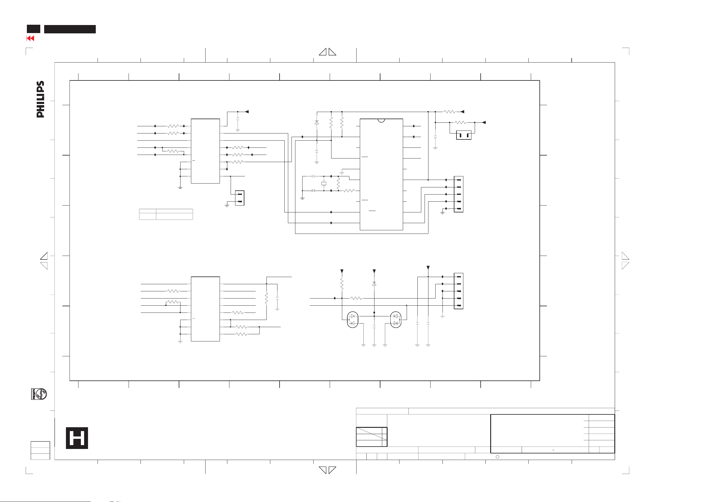
34
HP L2335
Go to cover page
Schematic diagram(I/O control)
2
4
6
7
81
935
10
123456789
A
NI
2735
100n
I412
I413
I414
I415
I416
3741
0R
3742
0R
1733
HEADER
1732
JFE6338V
1
2
3
4
5
+5V
12
7731
74LV4053PWT
C
B
A
DVI_SCL
DSUB_SCL_ROM
TXD_DDCCI
TXD
TXD_ISP
I393
I395
I398
100R3731
3732 100R
0R 3733
I394
I396
1
2Y1
2
2Y0
3
3Y1
4
3Z
5
3Y0
6
E
7
VEE
8
GND
VCC
1Y1
1Y0
16
15
2Z
14
1Z
3734 100R
13
I399
12
I400
11
S1
10
S2
I401
9
DDCCI_SW
S3
B
D D
ReservedRef Des
232270296001
3741
0R
2731
100R3735
100R3736
1734
HEADER
12
+5V
100n
I403I397
I404
DVI_SDA
DSUB_SDA_ROM
I402
2733
15p
2734
15p
6731
2732
BAS32L
100n
1731
3737
I406
HC49S
I407
I408
I409
10K
3739
12MHZ
3738
2M
10K
1
PWM3_CMP2
P0.0 PWM0
2
PWM2_P1.7
3
PWM1_P1.6
4
RST_P1.5
5
VSS
6
X1_P2.1
3740
7
X2_CLKOUT
100R
P2.0
8
INT1_P1.4
9
SDA_INT0
P1.3
10
SCL_T0
P1.2
7732 P87LPC764
P0.5_CMPREF
P0.1_CIN2B
P0.2_CIN2A
BRAKE
P0.3_CIN1B
AD0
P0.4_CIN1A
AD1
AD2
VDD
P0.6_CMP1
AD3
P0.7_T1
P1.0_TxD
P1.1_RxD
AUDIO_PW
20
I410
MUTE_OUT
19
I411
AUD_IN_SEL_A
18
AUD_IN_SEL_B
17
16
15
14
13
12
11
RXD_DDCCI
TXD_DDCCI
C
All rights reserved. Reproduction in whole or in parts
is prohibited without the written consent of the copyright
owner.
E
F
G
D
E
DSUB_SCL_ROM
RXD_ISP
RXD_DDCCI
RXD
RXD_ISP
2722
10u
+5V
2723
100n
I433
+3.3V
3K3
3721
BAV99-GS08
6721
7730
74LV4053PWT
1
2Y1
100R3724
2
2Y0
3
3Y1
0R3725
4
3Z
5
3Y0
6
E
7
VEE
8
GND
VCC
1Y1
1Y0
2Z
1Z
S1
S2
S3
16
15
14
13
12
11
10
9
DDCCI_SW
DSUB_SCL1
DSUB_SDA1
DSUB_SDA_ROM
3726
TXD_ISP
100R
470R3727
3728 100R
1K3729
DSUB_5V
2724
ISP_SW
100n
RXD
TXD
3722
1K
+3.3V
6722
2721
I435
LS4148
220n
6723
BAV99-GS08
I430
I431
I432
1721
JFE6336H
5
4
3
2
1
From / TO RS232
+3.3V
11
A
B
C
D
E
12
1721 D8
1731 B5
1732 B8
1733 A8
1734 C4
2721 E6
2722 E7
2723 E7
2724 D4
2731 A4
2732 A5
2733 B5
2734 B5
2735 A8
3721 D6
3722 D6
3724 D2
3725 D2
3726 E4
3727 E4
3728 E4
3729 D4
3731 A2
3732 A2
3733 A3
3734 A4
3735 B4
3736 B4
3737 A5
3738 A6
3739 B6
3740 B6
3741 A8
3742 A8
6721 E6
6722 D6
6723 E7
6731 A5
7730 E3
7731 A3
7732 A6
I393 A2
I394 A3
I395 A2
I396 A3
I397 A2
I398 A2
I399 A3
I400 A3
I401 B3
I402 A5
I403 A4
I404 B4
I406 B6
I407 B6
I408 C6
I409 C6
I410 A7
I411 A7
I412 B8
I413 B8
I414 B8
I415 B8
I416 C8
I430 D8
I431 D8
I432 D8
I433 D6
I435 E6
13
A
B
C
E
F
G
H
gedeeltelijk, is niet toegestaan dan met schriftelijke
toestemming van de auteursrechthebbende.
Alle rechten voorbehouden. Verveelvuldiging, geheel of
I
J
H
1
23456789
EXCEPT 1721,1732,1733,1734 WERE CHIP COMPONENTS.
CHN SETNAME WUH3 ( HPQ-230W Hanel )
TYT12-
CLASS_NO
1
I
--------
I/O CONTROL
SCALER BOARD
SB: 58421 x2
PB: 58431
1
3 11
4
5
68
7
2003-10-24 3
NAME
David Chiang/Edward Chang
IJ6B2W/76
SUPERS.
******** 2003-10-24
CHECKMGr DATE
9
11 8
10
3138 158 5732
13010 *** A3
C
KONINKLIJKE PHILIPS ELECTRONICS N.V. 2000
12
132
J
Page 35
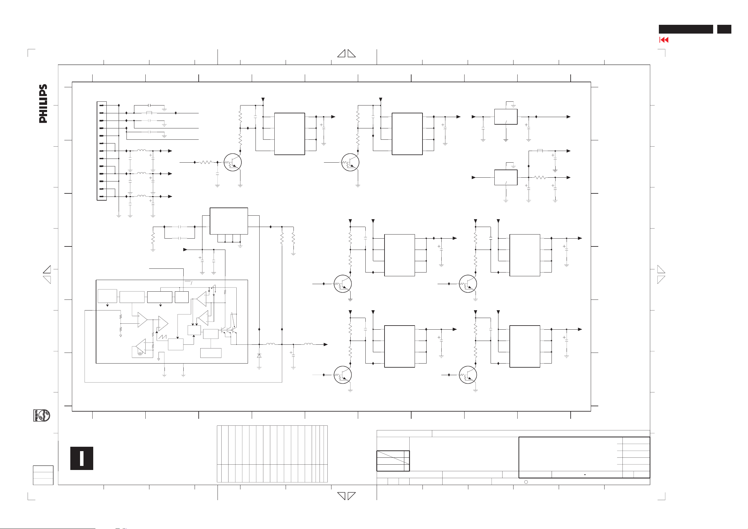
Schematic diagram(Power)
HP L2335
Go to cover page
35
A
B
C
D
All rights reserved. Reproduction in whole or in parts
is prohibited without the written consent of the copyright
owner.
E
F
G
H
gedeeltelijk, is niet toegestaan dan met schriftelijke
Alle rechten voorbehouden. Verveelvuldiging, geheel of
toestemming van de auteursrechthebbende.
I
1
2
43
12345
1751
A
B
C
D
E
63393
FROM POWER PCB
LM2596SX-5.0
CURRENT
SOURCE
FEEDBACK
4
3.3V , R2 = 4.2 K
12V , R2 = 21.8 K
I434
1
2
3
4
5
6
7
8
9
10
11
12
13
NI
7764
BIAS
R1=2.5K
5V,R2=7.6K
ADJ,R2=0R
R1 = OPEN
I468
I557
REFERENCE
R2
I464
I465
I466
I467
2753
2755
2777
1.235V
CAPACITOR
5754
10u
100n
5755
10u
100n
5756
10u
100n
AMP
ACTIVE
OP AMP
2751 100n
5752
100MHZBLM21
100n2757
2752 100n
2754
2756
2778
NI
3773
PWR_SAVING
REGULATOR
GM
I470
470u
I471
470u
I558
470u
I498
4K7
2.5V
2.5V
COMP.
I469
BL_ENABLE
PWR_SAVING
+18V
+5V
+3.3V
2766
22n
2767
100n
+18V
START
UP
FREQ.
150KHZ
OSC.
GND1 MT1
3
BL_BRI
LCDPW
NI
NI
5
ON
SHIFT
6
10K
I472
3778
10u
2758
8
I499
45
COMP
GND02GND13GND267GND3
2768
2769
470u
220mV
OFF
+
+
COMP.
CURRENT
LIMIT
COMP.
LATCH
DRIVER
RESET
THERMAL
LIMIT
F
EXCEPT 1751,2754,2756,2759,2770,2778,5751,5753,5754,5755,5756 WERE CHIP COMPONENTS.
1
2
6 13
LCM18V
I476
8
D1
7
3777
2770
D2
6
D3
5
D4
1K8
5751
10u
NI
NI
470u
2760
TMDSTXPW
I482
+5V
TMDSRXPW
I490
47u
1V5
7
+5V
3775
3776
I483
+5V
3781
3782
3771100K
3772
I477
7772
MUN2211J
100K
10K
7776
MUN2211J
10K
I491
7782
MUN2211J
I473
100n
NI
7762
L5972D
1
Vin
SWITCH
3779
3780
3A
OUTPUT
I474
7769
MUN2211J
OUTVCC
FB
47K
I475
100K
5
+18V
7770
SI4835DY
1
S1
100n
2759
2
S2
3
S3
4
G
1
I501
NI NI
5K6
3774
35uH
6751
NI
5753
NI
I502
I500
2
2
SS34
1
345
100K
10K
2775
2781
3
2762
3
2763
7777
SI4835DY
7791
SI4835DY
11
I480
47u
I481
47u
D1
D2
D3
D4
D1
D2
D3
D4
5763
100MHZ
3785
18R
2764
2765
8
I489
7
6
5
I497
8
7
6
5
9
67
+3.3V
7771
I478
2771
+5V
100n
+5V
100n
I492
I484
100n
SI4835DY
1
S1
2
S2
3
S3
4
G
7775
SI4835DY
1
S1
2
S2
3
S3
4
G
7781
SI4835DY
1
S1
2
S2
3
S3
4
G
8
D1
7
D2
6
D3
5
D4
8
D1
7
D2
6
D3
5
D4
I493
8
D1
7
D2
6
D3
5
D4
I479
I485
2772
TMDSTX5V
47u
2776
VIDEOPW
I486
TMDSRX5V
47u
2782
ADCPW
I494
+3.3V_S
47u
+3.3V_S
AME8815AEGT150
+3.3V
+5V
3783
3784
+5V
3791
3792
108
89
7761
IRU1206-25CY
4
1
Vi
Vo
GND
ADJ
2
100n
2761
7763
100K
5K1
I487
7778
MUN2211J
100K
10K
I495
7792
MUN2211J
2773
2792
4
1
Vi
Vo
GND
ADJ
2
+5V
1
S1
100n
2
S2
3
S3
I488
4
G
+5V
1
S1
100n
2
S2
3
S3
I496
4
G
6789
+2.5V
47u
1V5PLL
47u
1V5
2774
2791
12
VIDEO5V
47u
ADC5V
47u
A
B
C
D
E
F
1751 A1
2751 A1
2752 A1
2753 B1
2754 B2
2755 B1
2756 B2
2757 A1
2758 B3
2759 A4
2760 A5
2761 A8
2762 A9
2763 B9
2764 B9
2765 B9
2766 C2
2767 C2
2768 D3
2769 D2
2770 F4
2771 A6
2772 A7
2773 C8
2774 D9
2775 C6
2776 D7
2777 C1
2778 C2
2781 E6
2782 E7
2791 E9
2792 E8
3771 A5
3772 A5
3773 C2
3774 C4
3775 C5
3776 D5
3777 C4
3778 B3
3779 A3
3780 A3
3781 E5
3782 E5
3783 C8
3784 D8
3785 B9
3791 E8
3792 E8
5751 E5
5752 A2
5753 E4
5754 B1
5755 B1
5756 C1
5763 B9
6751 F4
7761 A8
7762 C3
7763 B8
7764 D1
7769 B3
7770 A4
7771 A6
7772 B6
7775 C6
7776 D5
7777 C9
7778 D8
7781 E6
7782 F5
7791 E9
7792 F8
I434 A1
I464 A1
I465 A1
I466 A1
I467 B1
I468 B1
I469 A2
I470 B2
I471 B2
I472 B2
I473 B3
I474 B3
I475 A3
I476 A5
I477 B6
I478 A6
I479 A7
I480 A9
I481 B9
I482 D5
I483 D5
I484 D6
I485 C7
I486 D7
I487 D8
I488 D8
I489 C9
I490 F5
I491 F5
I492 F6
I493 E7
I494 F7
I495 F8
I496 F8
I497 E9
I498 C2
I499 C2
I500 E4
I501 C4
I502 E4
I557 C1
I558 C2
A
B
C
D
E
F
G
H
I
TYT12-
CLASS_NO
J
1
SCALER BOARD
SB: 58421 x2
PB: 58431
2
35uH
SS34
6751 932208282668
7762 932219076668
932215923668
L5972D
7764
icct_dia009_t
I502 icct_dia009_t
I500 icct_dia009_t
I501
I499 icct_dia009_t
2003-10-24
David Chiang/Edward Chang
NAME
7
8
232273461802
1K8
22n
2238580156412766
ReservedRef Des
100n
100n
470u
470u
4K7
2767 222258015649
2768 223878615649
2769 202203100068
2770 202203100068
3773 319802154720
43
5
232273465602
5K6
5751 242253594969
3777
3774
10u
5753 313818875691
LM2596SX-5.0
POWER SUPPLY
IJ6B2W/76
3
SUPERS.
DATEMGr CHECK
9
WUH3 ( HPQ-230W Hanel )SETNAMECHN
--------
1
3138 158 5732
911
2003-10-24********
10
C
KONINKLIJKE PHILIPS ELECTRONICS N.V. 2000
116
12
13
J
A3***10 130
Page 36
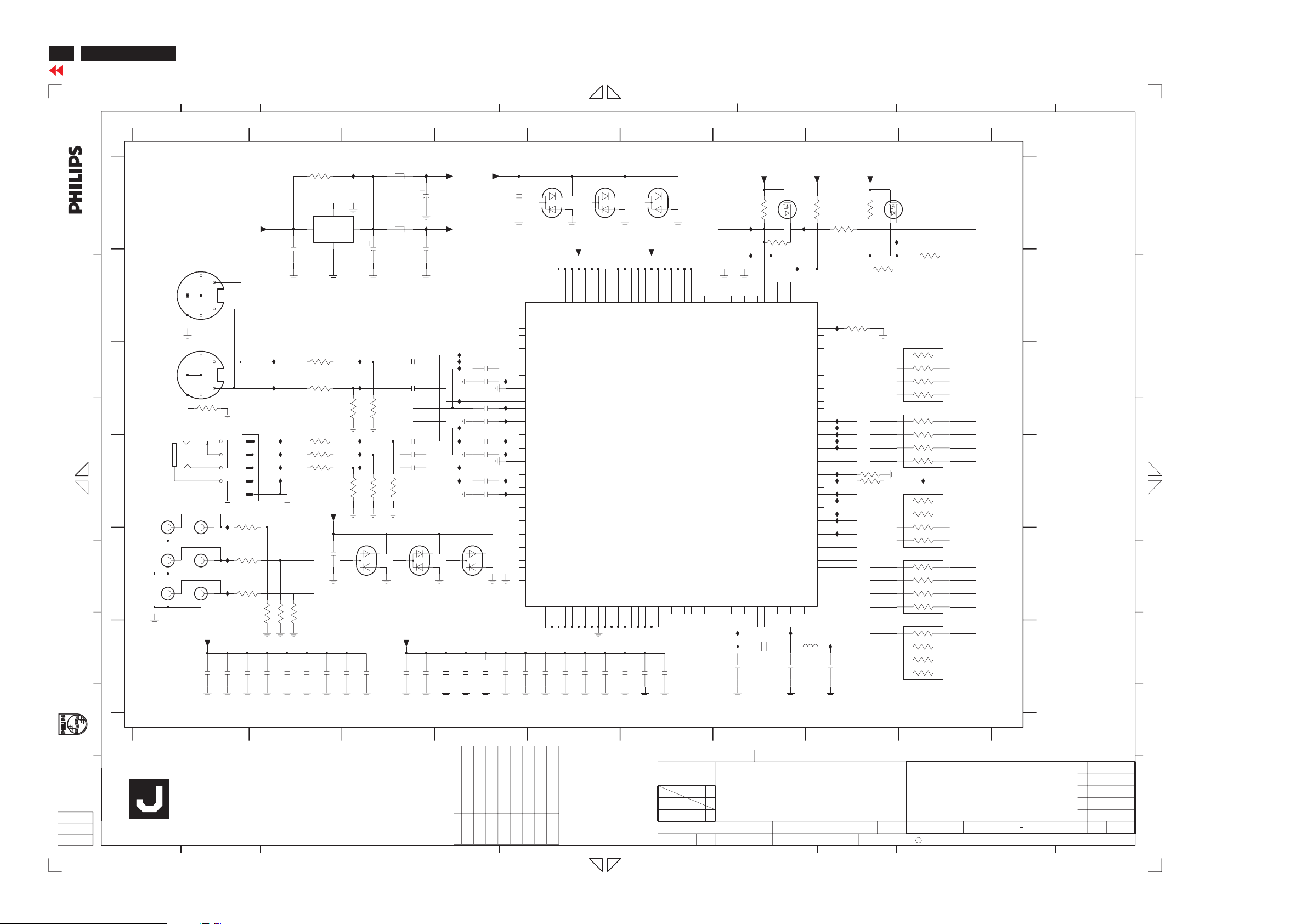
36
HP L2335
Go to cover page
Schematic diagram(Video decoder)
A
B
C
D
All rights reserved. Reproduction in whole or in parts
is prohibited without the written consent of the copyright
owner.
E
F
G
H
gedeeltelijk, is niet toegestaan dan met schriftelijke
Alle rechten voorbehouden. Verveelvuldiging, geheel of
toestemming van de auteursrechthebbende.
I
1
2
12
A
VIDEO5V
2601
35
1607
B
69015
1602
69015
S-VIDEO
C
1603
CVBS
61138
D
1
3
5
2
1605-A
69040
4
1605-B
6
1605-C
69040
69040 3
DVDA
E
1608-A
69040
1608-B
69040
1608-C
69040
F
EXCEPT 1602,1603,1604,1605,1607,1608 WERE CHIP COMPONENTS.
12
4
124
G
35
3633
0R
1
5
2621 100n
68
I507
Y-S
68
I508
C-S
1604
63135
4
3
2
1
2
4
6
3625
I526
3626
I527
3627
I528
100n2622
2623 100n
CVBS
1
I522
2
I523
3
I524
4
I525
5
NI
0R
0R
0R
3628
362975R
75R
75R 3630
100n2624
100n2625
43
NI
3601
1206
LM2937IMP-3.3
1
100n
3602 47n2605
3603
3606 18R
3608 18R
R-PR
B-PB
G-Y
100n2626
I504 I505
0R
7602
4
Vi
2627 100n
3
Vo
GND
2
18R
18R
18R3607
NI
NI
+3.3V
G-Y
220n
2645
BAV99-GS08 BAV99-GS08
2628 100n
3604
3609 56R
I509
I510
I519
I520
I521
6604
56R
2629 10u
2602
NINI
3605
56R3610
47u
56R
5
6
7
34567
5601
100MHZ
1206
5602
100MHZ
1206
2606 47n
2615 47n
2617 47n
3611 56R
B-PB R-PR
BAV99-GS08
OVDD
100n
2630
2604
I506
2603
G-Y
B-PB
47n2616
R-PR
DVDA
47u
OVDD
47u
100n2631
2632 100n
I514
I511
I513
I512
I515
I516
I517
I518
2611 47n
66066605
2633 100n
+3.3V
2608 47n
2612 47n
100n2634
OVDD
Y-S C-S CVBS
220n
3K3
D6
M12
TMS
AMXCLK
N13
N14
2618
I541
P11
AMCLK
RES12
RES13
P2
I536
22p
3612
P12
P10
N11
SDA
ASCLK
ALRCLK
XTOUT
XTAL
XTALI
A3
B4
A2
1606
24M576HZ
3613
0R05
N9
SCL
TEST0
P13
2644
6601
BAV99-GS08
K4
H4
L10
RTCO
N10
RTS1
M10
RTS0
N5
LLC2
P4
I529
I530
I531
I532
I533
I534
I535
100n2635
K1
K2
L3
K3
C2
G4
G3
H2
H1
E3
F2
F3
G1
F1
L2
B1
D2
D1
E1
D3
P3
M1
N8
P8
M7
L7
P7
N7
L6
M6
P6
N6
M13
J2
J3
2636 100n
LLC
AI11
AI12
AI13
AI14
AI1D
AGND
AI21
AI22
AI23
AI24
AI2D
AI31
AI32
AI33
AI34
AI3D
AGNDA
AI41
AI42
AI43
AI44
AI4D
EXMCLR
AOUT
ADP0
ADP1
ADP2
ADP3
ADP4
ADP5
ADP6
ADP7
ADP8
CLKEXT
FSW
47n2607
47n2609
47n2610
47n2613
47n2614
VSSA0
VSSA1
J4
M2
100n2637
VDDA2
VDDA0M3VDDA1
VSSA2H3VSSA3E4VSSA4
C1
2638 100n
F4
D4
VDDA3
VDDA4
VSSI1D7VSSI2
D10
2639 100n
6602
BAV99-GS08
DVDA
J1
L1
E2
G2
VDDA4A
VDDA1A
VDDA3A
VDDA2A
VSSI3
VSSI4
VSSI5
L5
L9
J11
F11
2640 100n
C10
VDDI1C8VDDI2
VSSI6
VSSE1D5VSSE2D9VSSE3
100n2641
J12
F12
VDDI3
VDDI4
D11
G11
BAV99-GS08
M9
VDDI5M5VDDI6
VSSE4
VSSE5L4VSSE6L8VSSE7
100n2642
6603
OVDD
C5
D12
H12
VDDE1
VDDE2C9VDDE3
VDDE4
VDDE5M4VDDE6M8VDDE7
7601
SAA7118E/V1
VXSS
RES4
RES1
RES2
RES3
A4
B2
C3
L11
B13
B14
10u2643
M11
C4
B3
VXDD
RES5
C12
A5
TDO
RES6
C13
B5
TDI
RES7
VSDA
VSCL
B6
C6
TCK
TRSTN
RES8N1RES9
N2
RES10N3RES11
P9
INT_A
TEST1
D13
I537
N4
CE
TEST2
C14
2619
7603
I543I540
NI
I542
P5
RESON
XRDY
XCLK
XPD0
XPD1
XPD2
XPD3
XPD4
XPD5
XPD6
XPD7
HPD0
HPD1
HPD2
HPD3
HPD4
HPD5
HPD6
HPD7
ITRDY
TEST3
TEST4
A13
B12
22p
2N7002 LT1
XTRI
XRV
XRH
XDQ
ITRI
IGP1
IGP0
IGPV
IGPH
IDQ
ICLK
IDP0
IDP1
IDP2
IDP3
IDP4
IDP5
IDP6
IDP7
TEST5
A12
5603
0805
OVDD
10u
3615
B11
D8
C7
A6
B7
A7
A8
B8
A9
B9
A10
B10
A11
C11
D14
E11
E13
E12
E14
F13
F14
G13
L12
K13
L14
K14
K12
N12
L13
M14
G14
G12
H11
H14
H13
J14
J13
K11
10K
3614
100R
VIDEO_CE
I539
I552
I553
I554
I555
I556
I545
I546
I548
I549
I550
I551
I561
I538
1n
2620
10
11
1289
89
OVDD
7604
2N7002 LT1
3K3
3616
SDA
I544
3617
NI
0R05
3619
10K
IDP0
1
IDP1
2
IDP2
3
IDP3 VY3
45
HPD0
HPD1
HPD2
HPD3
HPD4
HPD5
HPD6
HPD7
3620
3624
IGPV
IGPH
IDQ
ICLK
IDP0
IDP1
IDP2
IDP3
IDP4
IDP5
IDP6
IDP7
1
IDP4
2
IDP5
3
IDP6
45
IDP7 VY7
10K
47R
IGPV
1
IGPH
2
IDQ
ICLK
HPD0
HPD1
HPD2
HPD3 VUV3
HPD4
HPD5
HPD6
HPD7 VUV7
3623 47R
3
45
1
2
3631 47R
3
45
1
2
3
45
3618
100R
R
R
R
R
R
R
R
R
I547
R
R
R
R
R
R
R
R
R
R
R
R
SCL
VY0
8
VY1
7
47R3621
VY2
6
8
VY4
7
VY5
47R3622
6
VY6
VFIELD
8
VVS
7
VHS
VPEN
6
VCLK
VUV0
8
VUV1
7
VUV2
6
VUV4
8
VUV5
7
47R3632
VUV6
6
A
B
C
D
E
F
1602 B1
1603 D1
1604 C2
1605-A E1
1605-B E1
1605-C E1
1606 F7
1607 B1
1608-A D1
1608-B E1
1608-C E1
2601 B2
2602 B3
2603 B3
2604 A3
2605 C3
2606 C3
2607 C4
2608 C4
2609 C4
2610 C4
2611 D4
2612 D4
2613 D4
2614 D4
2615 D3
2616 D3
2617 D3
2618 F7
2619 F7
2620 F8
2621 F1
2622 F1
2623 F1
2624 F2
2625 F2
2626 F2
2627 F2
2628 F2
2629 F3
2630 F3
2631 F3
2632 F4
2633 F4
2634 F4
2635 F4
2636 F4
2637 F5
2638 F5
2639 F5
2640 F5
2641 F5
2642 F6
2643 F6
2644 A4
2645 E2
3601 A2
3602 C2
3603 C2
3604 C3
3605 C3
3606 D2
3607 D2
3608 D2
3609 D3
3610 D3
3611 D3
3612 A7
3613 A7
3614 A8
3615 A8
3616 A8
3617 B8
3618 B9
3619 B8
3620 D8
3621 C9
3622 D9
3623 D9
3624 D8
3625 D1
3626 E1
3627 E1
3628 E2
3629 E2
3630 E2
3631 E9
13
3632 F9
3633 C1
5601 A3
5602 A3
5603 F8
6601 A5
6602 A5
6603 A6
6604 E3
6605 E3
6606 E4
7601 D6
7602 A2
7603 A7
7604 A9
I504 A3
I505 A3
I506 A3
I507 C2
I508 C2
I509 C3
I510 C3
I511 C4
I512 C4
I513 C4
I514 C4
I515 C4
I516 D4
I517 D4
I518 D4
I519 D3
I520 D3
I521 D3
I522 D2
I523 D2
I524 D2
I525 D2
I526 E1
I527 E1
I528 E1
I529 C4
I530 C4
I531 C4
I532 D4
I533 D4
I534 D4
I535 D4
I536 F7
I537 F7
I538 F8
I539 B8
I540 A7
I541 B7
I542 B7
I543 A8
I544 A9
I545 D8
I546 D8
I547 D9
I548 D8
I549 D8
I550 D8
I551 D8
I552 C8
I553 C8
I554 C8
I555 D8
I556 D8
I561 E8
A
B
C
D
E
F
G
H
I
1
J
SCALER BOARD
SB: 58421 x2
PB: 58431
1
23456789
TYT12-
CLASS_NO
WUH3 ( HPQ-230W Hanel )SETNAMECHN
VIDEO DECODER
232270260569
0R05
3198021900303617
3610
56R
3198021900303613
0R05
32003-10-24
NAME
David Cuiang/Edward Chang
7
8910
IJ6B2W/76
SUPERS.
DATECHECK
2003-10-24
232270260189
232270260189
18R
56R
18R
header-v5x1p
63135
3608
Ref Des Reserved
3601 2322711910320R3607
1604
4
56
3609 232270260569
3138 158 5732
130
C
KONINKLIJKE PHILIPS ELECTRONICS N.V. 2000
11 12 1323
1
--------
J
1011
A3
Page 37

Schematic diagram(HDTV-decoder)
HP L2335
Go to cover page
37
A
B
C
D
All rights reserved. Reproduction in whole or in parts
owner.
is prohibited without the written consent of the copyright
E
F
G
H
gedeeltelijk, is niet toegestaan dan met schriftelijke
Alle rechten voorbehouden. Verveelvuldiging, geheel of
toestemming van de auteursrechthebbende.
I
A
B
C
D
E
F
21
43 12
12345
5651
VIDEO5V
2668
PVD
100n
3653
2651
2K2
Vin
100n
R-PR
G-Y
B-PB
VSCL
VSDA
16
2666
3n9
2667
39n
7651
LM1117MPX-3.3
4
MT1
3
ADJ
GND
1
2
3651
2K2
3652
3K3
2669
2670
2671
2672
3654
3655
Vout
4n7
4n7
4n7
1n
100R
100R
2652
10u
I629
I630
I631
I632
I633
I637
I638
I639
2673
I625
29
30
31
33
37
38
54
48
43
49
55
56
57
58
100n
100MHZ
BEAD
5652
100MHZ
BEAD
5653
100MHZ
BEAD
COAST
HSYNC
VSYNC
FILT
MIDSCV
CLAMP
Rain
Gain
Bain
SOGIN
A0
SCL
SDA
REF_BYPASS
5
I626
I627
I628
11
VDD022VDD123VDD269VDD378VDD479VDD5
GND221GND324GND425GND528GND6
GND010GND1
1
20
10u
2654
2653
10u
2659
2658
10u
2663
2664
27
26
VD139VD242VD345VD446VD551VD652VD759VD862VD9
VD0
7652
AD9883A
GND736GND840GND9
GND1147GND1250GND1353GND1460GND1561GND1663GND1768GND1880GND19
GND10
32
41
44
100n
100n
100n
2655
2660
2665
6
7
8
6789
I596
2656
100n
2657
2661
35
PVD1
100n
2662
DATACK
HSOUT
VSOUT
SOGOUT
RED7
RED6
RED5
RED4
RED3
RED2
RED1
RED0
GREEN7
GREEN6
GREEN5
GREEN4
GREEN3
GREEN2
GREEN1
GREEN0
BLUE7
BLUE6
BLUE5
BLUE4
BLUE3
BLUE2
BLUE1
BLUE0
PVD
100n
100n
2674
67
66
64
65
70
71
72
73
74
75
76
77
2
3
4
5
6
7
8
9
12
13
14
15
16
17
18
19
100n
3656
100R
I597
I598
I600
I601
I602
I603
I604
I605
I606
I607
I608
I609 I581
I610
I611
I612
100n
100n
100n
34
PVD0
123456
9
3657 47R
1
2
3
45
3658
45
3
2
1
45
3
2
1
3660 47R
45
3
2
1
45
3
2
I615
1
3662 47R
I616
45
I617
3
I618
2
I619
1
I620
45
I621
3
I622
2
I623
1
R
R
R
R
47R
R
R
R
R
R
R
R
R
R
R
R
R
47R3661
R
R
R
R
R
R
R
R
R
R
R
R
8
7
6
6
7
8
47R3659
6
7
8
6
7
8
6
7
8
6
7
8
47R3663
6
7
8
10
I568
I569
I570
I571
I572
I573
I574
I575
I576
I577
I578
I579
I580
I582
I583
I584
I585
I586
I587
I588
I589
I590
I591
I592
I593
I594
I595
VCLK
VHS
VVS
GSOG
VR7
VR6
VR5
VR4
VR3
VR2
VR1
VR0
VY7
VY6
VY5
VY4
VY3
VY2
VY1
VY0
VUV7
VUV6
VUV5
VUV4
VUV3
VUV2
VUV1
VUV0
11
78
13
I615 E7
I616 E7
I617 E7
I618 E7
I619 F7
I620 F7
I621 F7
I622 F7
I623 F7
I625 A3
I626 A4
I627 A4
I628 B4
I629 C3
I630 D3
I631 D3
I632 D3
I633 D3
I637 E3
I638 E3
I639 E3
A
B
C
D
E
F
G
H
A
B
C
D
E
F
2651 B2
2652 B3
2653 A4
2654 A4
2655 A4
2656 A5
2657 A5
2658 B4
2659 B4
2660 B4
2661 B5
2662 B5
2663 B5
2664 B5
2665 B5
2666 C2
2667 D2
2668 D1
2669 D2
2670 D2
2671 D2
2672 D2
2673 E3
2674 B5
3651 C2
3652 D2
3653 D1
3654 E2
3655 E2
3656 C6
3657 B7
3658 C7
3659 C7
3660 D7
3661 D7
3662 E7
3663 F7
5651 A3
5652 A3
5653 B3
7651 A2
7652 D4
I568 B8
I569 B8
I570 B8
I571 B8
I572 C8
I573 C8
I574 C8
I575 C8
I576 C8
I577 C8
I578 D8
I579 D8
I580 D8
I581 D8
I582 D8
I583 D8
I584 E8
I585 E8
I586 E8
I587 E8
I588 E8
I589 E8
I590 E8
I591 F8
I592 F8
I593 F8
I594 F8
I595 F8
I596 B7
I597 B7
I598 B7
I600 C7
I601 C7
I602 C7
I603 C7
I604 C7
I605 C7
I606 D7
I607 D7
I608 D7
I609 D7
I610 D7
I611 D7
I612 E7
I
9
TYT12-
CHN
CLASS_NO
J
SCALER BOARD
SB: 58421 x2
PB: 58431
1
2 13
3
4
5
6
7
2003-10-24 3
David Chiang/Edward Chnag
NAME
CHECK DATE
SETNAME WUH3 (HPQ-230W Hanel )
HDTV DECODER
IJ6B2W/76
SUPERS.
2003-10-24
9
10
3138 158 5732
11 11
C
KONINKLIJKE PHILIPS ELECTRONICS N.V. 2000
11
130 A3
128
--------
1
J
Page 38

Page 39

Page 40
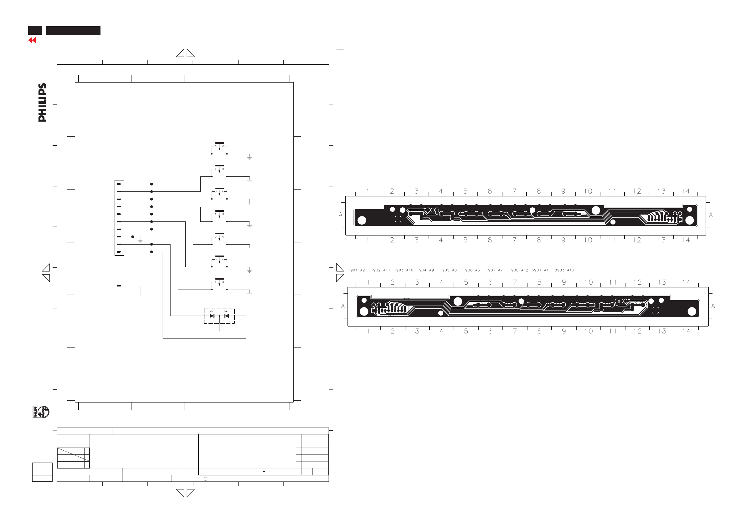
40
HP L2335
Go to cover page
Control board C.B.A.
All rights reserved. Reproduction in whole or in parts
is prohibited without the written consent of the copyrightHowner.
C
D
A
B
E
F
A
B
C
D
1
2
1
CONTROL BOARD
SB: 59791 x10
PB: 59801
1901
63370
TO SCALER BOARD
10
8903
JFE63041
1
3
2
F951
F952
F953
F954
F955
F956
F957
F959
F960
MENU
UP
DOWN
AUTO
PIP
INPUT
DC-SWI
1
2
3
4
5
6
7
F958
8
9
4
3
1902
SKHHAR2520
4
1903
SKHHAR2520
4
1904
SKHHAR2520
4
1905
SKHHAR2520
4
1906
SKHHAR2520
4
1907
SKHHAR2520
4
1908
SKHHAR2520
4
6901
L-3WYGW
12
3
12
3
12
3
12
3
12
3
12
3
12
3
56
A
B
1901 B1
1902 A3
1903 B3
1904 B3
1905 C3
1906 C3
1907 D3
1908 D3
6901 E3
8902 D1
8903 E1
F951 B2
F952 B2
F953 C2
F954 C2
F955 C2
F956 C2
F957 C2
F958 C2
F959 C2
F960 D2
A
B
C
4
D
C
E
D
F
G
Alle rechten voorbehouden. Verveelvuldiging, geheel of
gedeeltelijk, is niet toegestaan dan met schriftelijke
toestemming van de auteursrechthebbende.
H
I
J
CLASS_NO
NAME
E
F
12
TYT12-
CONTROL BOARD
32003-10-24
Devid
IJ6B2W/76
SUPERS.
DATECHECK
12
WUH3 ( HPQ-230W Hanel )SETNAMECHN
2003-10-24
G
3
1
2
K
Y
E
G
F
34
--------
1
3138 158 5674
11
C
KONINKLIJKE PHILIPS ELECTRONICS N.V. 2000
3
4
5
6
I
J
A4130
Page 41

江碩桓閻本孝
代
Page 42
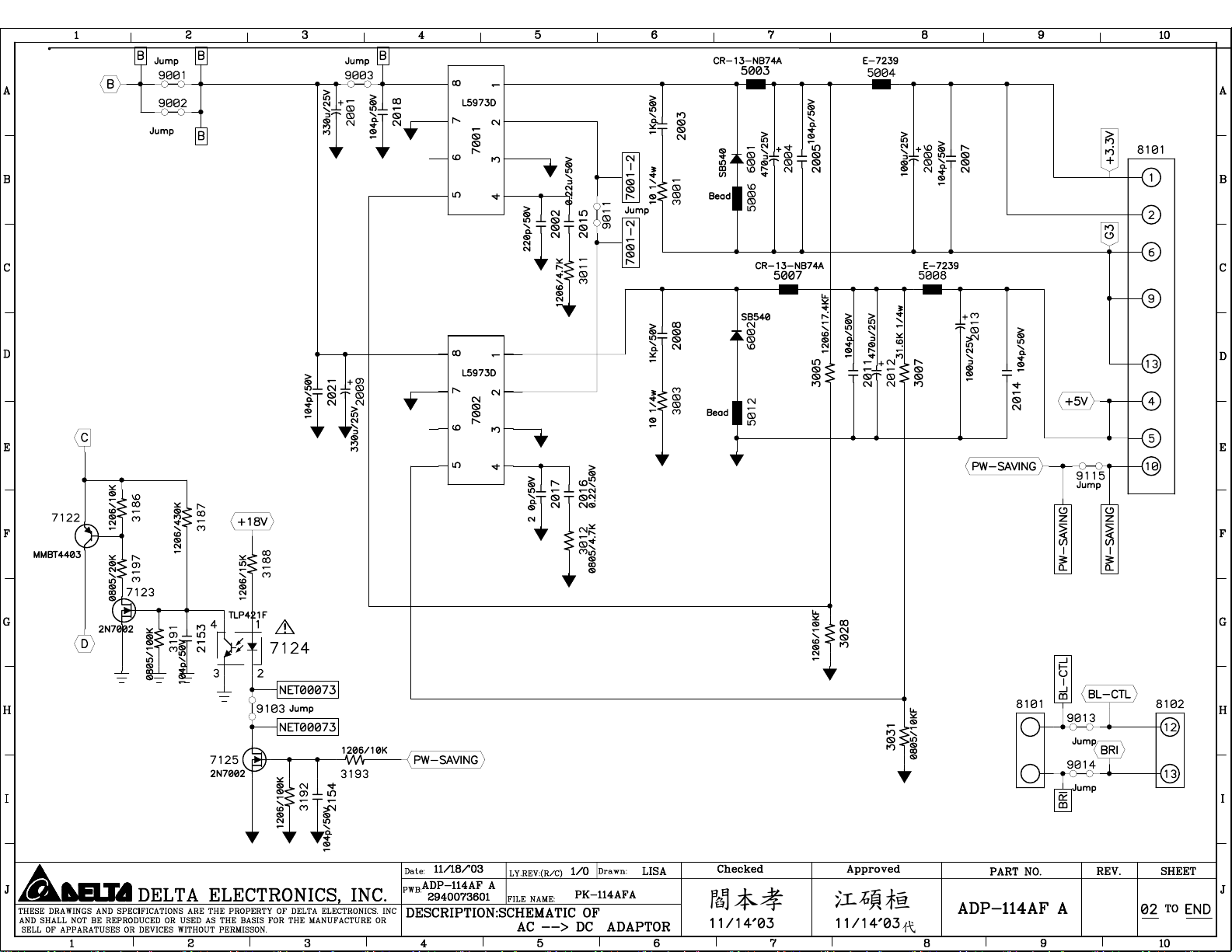
江碩桓閻本孝
代
Page 43

Page 44

44
HP L2335
Go to cover page
Repair Flow Chart
Chassis debug
Check
DC_supplies
Check
Key_scan
Check
oscillator
- Confirm CPU operation
- Check signal paths
- Check PLL_clocks
- Check panel v, CLK ,data, controls
- Fix any abnormal
Fix defects
Fix defects
Fix defects
Level 1:
DC power_3.3V
5.0V
1.8V
CPU Reset IC
+3.3V(7401)
Scaler power
LED -G
off
Ye s
Display
No
Crystal signal
+3.3V_D(5405,5406)
check crystal(
Check LED
Check IC 7480
Check resisters
Check Solder Status
EEPROM(7472)
+3.3V
1410)
Flash Memory
+3.3V(7471)
Page 45

Repair Flow Chart
No Display
HP L2335
Go to cover page
45
Level 2:
Back light
control signals
Scaler signals
CLK
STV
STH
Level 1?
Input signals
Schmitt trigger
resisters
No
Ye s
EEPROM
I2C SCL
I2C SDA
Panel power
Panel_PWR
3.3V(7771,7761,7763)
18V(7770)
5V(7775,7776)
Go to level 1
Flash Memory
ADDRESS bus
DATA bus
Check components
-Scaler
-EEPROM
-Flash Memory
-Schmitt trigger
Level 1
Ye s
Level 2
Ye s
Check wires
-FFC
-Key pad wire
-Wire to power board
-DDC
Page 46
46
Go to cover page
HP L2335
Repair Flow Chart
Power on
Power on
LED
LED
Amber
Amber
Check cable connection
Check cable connection
or system into DPMS
or system into DPMS
see display message
see display message
Display picture
Display picture
Check back_light_inverter
Check back_light_inverter
- Brightness
- Brightness
- BL_control
- BL_control
- Panel_IDX
- Panel_IDX
Adjustment
Green
Green
Ye sNo
Ye sNo
Go to Adjustment
Go to Adjustment
OFF
OFF
Go to chassis Debug
Go to chassis Debug
END adjustment
yes
OK
Activate Auto_adj
Good picture ?
no
preset mode ?
yes
Manual adjust
- Clock
- Phase
- Position
Set default mode
no
no
Go to chassis Debug
Page 47
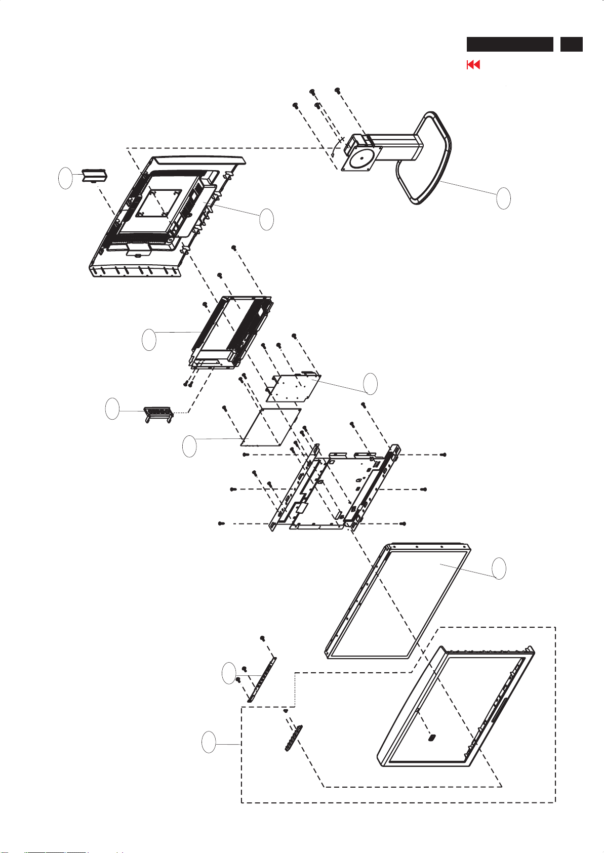
45
313815410881
VIDEO-OUTER COVER
Exploded View
41
313815410871
BACK COVER
HP L2335
Go to cover page
50
313815755871
STAND
47
313815134811
MAIN SHIELD
91
313815410891
VIDEO-INNER COVER
90
313815857321
SCALER ASSY
1053
823827714191
AC/DC POWER BOARD(ADP-114AF A)
1065
823827714381
TFT-LCD LC230W02
1074
313815856741
1051
30
313815755781
FRONT BEZEL ASSY
CONTROL ASSY
Page 48

48
HP L2335
Go to cover page
Spare parts List
Model:IJ6B2W/76 863900015025
Mechanical Parts
30 313815755781 FRONT BEZEL ASSY
41 313815410871 BACK COVER
45 313815410881 VIDEO-OUTER COVER
50 313815755871 STAND
91 313815410891 VIDEO-INNER COVER
98 313815561881 FRONT COVER
LCD Panel
1074 823827714381 TFT-LCD LC230W02
Packing
450 313815636201 CARTON
451 313815636181 CUSHION-R
452 313815636191 CUSHION-L
453 313810645302 P.E. BAG
Accessory
601 313811706042 HP CD-ROM INF.
1073 313812874901 MAINSCORD
1076 313819870261 CBLE-012 24/50/24-030 AWG28
1077 823827714071 DSUB INTERFACE CABLE 1.8M
1078 313818872251 CORD DVI 1M8 SUB-D F 15 BLK
1081 313816878931 I/F DVI CABLE (CE101320063710)
4444 313810610339 CD ROM - SERVICE MANUAL
4444 313810610340 SERVICE MANUAL
PCB Assy
1051 313815856741 CONTROL ASSY
1053 313815857321 SCALER ASSY
1065 823827714191 AC/DC POWER BOARD(ADP-114AF A)
Miscellanea
97 313810440571 HOUSING COVER
291 313815561861 LABEL-AD9888
295 313815561861 LABEL-AD9888
301 313815134801 MAIN FRAME
303 313815411581 INSULATING PLATE
304 313815412011 GASKET(300X6X6)
305 313815411991 GASKET(200X6X6)
615 313811706181 HEX CODE OF F/W-AD9888L REQ)
616 313811706191 HEX CODE OF F/W-MST9888
1075 313815857381 MAIN FRAME+WIRE ASSY
1391 313815857491 IC ASSY(7301)
1401 243854300086 RES XTL SM 14M318 18P HC49/S R
1602 243803100431 SOC MDIN H 4P F 69015 B
1603 242202605389 SOC CINCH H 1P F 1L1 YE B
1605 242202605453 SOC CINCH H 3P F 1L3 RDBUGR B
1606 243854300089 RES XTL SM 24M576 16P HC49/S R
8061 313819870251 CBLE-023 10/150/10-020 AWG28
8903 313818874422 CBLE RING TERM/100/FAST AWG18
PCB Assy-LG
1053 313815857321 SCALER ASSY
2201 223886715339 CER1 0603 NP0 50V 33P PM5 R
2202 223824615654 CER2 0603 X7R 10V 220N PM10 R
2203 223886715331 CER1 0603 NP0 50V 330P PM5 R
2204 223886715339 CER1 0603 NP0 50V 33P PM5 R
2205 223886715331 CER1 0603 NP0 50V 330P PM5 R
2206 223886715339 CER1 0603 NP0 50V 33P PM5 R
2207 223824615654 CER2 0603 X7R 10V 220N PM10 R
2209 223878615649 CER2 0603 X7R 16V 100N PM10 R
2215 223878615649 CER2 0603 X7R 16V 100N PM10 R
2216 223878615649 CER2 0603 X7R 16V 100N PM10 R
2217 223878615649 CER2 0603 X7R 16V 100N PM10 R
2218 223886715339 CER1 0603 NP0 50V 33P PM5 R
2219 223886715339 CER1 0603 NP0 50V 33P PM5 R
2222 223886715109 CER1 0603 NP0 50V 10P PM5 R
2223 223886715109 CER1 0603 NP0 50V 10P PM5 R
2224 222224119876 CER2 1206 Y5V 10V 10U P8020 R
2225 223824615654 CER2 0603 X7R 10V 220N PM10 R
2226 223886715331 CER1 0603 NP0 50V 330P PM5 R
2227 223886715331 CER1 0603 NP0 50V 330P PM5 R
2241 223878615649 CER2 0603 X7R 16V 100N PM10 R
2242 223878615649 CER2 0603 X7R 16V 100N PM10 R
2251 223878615649 CER2 0603 X7R 16V 100N PM10 R
2252 202202000781 ELCAP SM RV2 25V 47U PM20 R
2253 222224119876 CER2 1206 Y5V 10V 10U P8020 R
2254 223878615649 CER2 0603 X7R 16V 100N PM10 R
2255 202202000781 ELCAP SM RV2 25V 47U PM20 R
2256 222224119876 CER2 1206 Y5V 10V 10U P8020 R
2257 223878615649 CER2 0603 X7R 16V 100N PM10 R
2258 202202000781 ELCAP SM RV2 25V 47U PM20 R
2259 222224119876 CER2 1206 Y5V 10V 10U P8020 R
2261 223878615649 CER2 0603 X7R 16V 100N PM10 R
2262 223878615649 CER2 0603 X7R 16V 100N PM10 R
2263 223878615649 CER2 0603 X7R 16V 100N PM10 R
2264 223878615649 CER2 0603 X7R 16V 100N PM10 R
2265 223878615649 CER2 0603 X7R 16V 100N PM10 R
Spare Parts List
2266 223878615649 CER2 0603 X7R 16V 100N PM10 R
2267 223878615649 CER2 0603 X7R 16V 100N PM10 R
2268 223878615649 CER2 0603 X7R 16V 100N PM10 R
2269 223878615649 CER2 0603 X7R 16V 100N PM10 R
2270 223878615649 CER2 0603 X7R 16V 100N PM10 R
2271 223878615649 CER2 0603 X7R 16V 100N PM10 R
2272 223878615649 CER2 0603 X7R 16V 100N PM10 R
2273 223878615649 CER2 0603 X7R 16V 100N PM10 R
2274 223878615649 CER2 0603 X7R 16V 100N PM10 R
2275 223878615649 CER2 0603 X7R 16V 100N PM10 R
2276 223878615649 CER2 0603 X7R 16V 100N PM10 R
2277 223878615649 CER2 0603 X7R 16V 100N PM10 R
2278 223878615649 CER2 0603 X7R 16V 100N PM10 R
2279 223878615649 CER2 0603 X7R 16V 100N PM10 R
2280 223878615649 CER2 0603 X7R 16V 100N PM10 R
2281 223878615649 CER2 0603 X7R 16V 100N PM10 R
2282 223878615649 CER2 0603 X7R 16V 100N PM10 R
2283 223878615649 CER2 0603 X7R 16V 100N PM10 R
2284 223878615649 CER2 0603 X7R 16V 100N PM10 R
2285 223858015644 CER2 0805 X7R 50V 39N PM10 R
2286 223858015631 CER2 0805 X7R 50V 3N9 PM10 R
2287 223878615649 CER2 0603 X7R 16V 100N PM10 R
2288 223878615649 CER2 0603 X7R 16V 100N PM10 R
2289 223878615649 CER2 0603 X7R 16V 100N PM10 R
2290 223878615645 CER2 0603 X7R 16V 47N PM10 R
2291 223878615645 CER2 0603 X7R 16V 47N PM10 R
2292 223858615623 CER2 0603 X7R 50V 1N PM10 R
2293 223878615645 CER2 0603 X7R 16V 47N PM10 R
2294 223878615645 CER2 0603 X7R 16V 47N PM10 R
2295 223878615645 CER2 0603 X7R 16V 47N PM10 R
2296 223858615623 CER2 0603 X7R 50V 1N PM10 R
2297 223878615645 CER2 0603 X7R 16V 47N PM10 R
2301 223878615649 CER2 0603 X7R 16V 100N PM10 R
2302 202202000781 ELCAP SM RV2 25V 47U PM20 R
2303 222224119876 CER2 1206 Y5V 10V 10U P8020 R
2304 222224119876 CER2 1206 Y5V 10V 10U P8020 R
2305 222224119876 CER2 1206 Y5V 10V 10U P8020 R
2306 223878615649 CER2 0603 X7R 16V 100N PM10 R
2307 202202000781 ELCAP SM RV2 25V 47U PM20 R
2308 222224119876 CER2 1206 Y5V 10V 10U P8020 R
2309 223878615649 CER2 0603 X7R 16V 100N PM10 R
2310 223886715471 CER1 0603 NP0 50V 470P PM5 R
2311 223886715471 CER1 0603 NP0 50V 470P PM5 R
2312 223886715471 CER1 0603 NP0 50V 470P PM5 R
2313 223886715471 CER1 0603 NP0 50V 470P PM5 R
2314 223886715471 CER1 0603 NP0 50V 470P PM5 R
2315 223886715471 CER1 0603 NP0 50V 470P PM5 R
2316 223886715471 CER1 0603 NP0 50V 470P PM5 R
2317 223886715471 CER1 0603 NP0 50V 470P PM5 R
2318 223886715471 CER1 0603 NP0 50V 470P PM5 R
2319 223886715471 CER1 0603 NP0 50V 470P PM5 R
2320 223886715471 CER1 0603 NP0 50V 470P PM5 R
2321 223886715471 CER1 0603 NP0 50V 470P PM5 R
2322 223878615649 CER2 0603 X7R 16V 100N PM10 R
2341 223878615649 CER2 0603 X7R 16V 100N PM10 R
2401 223886715189 CER1 0603 NP0 50V 18P PM5 R
2402 223886715189 CER1 0603 NP0 50V 18P PM5 R
2405 202203100205 ELCAP SM RVS 25V 47U PM20 R
2406 202203100205 ELCAP SM RVS 25V 47U PM20 R
2408 223878615649 CER2 0603 X7R 16V 100N PM10 R
2409 223878615649 CER2 0603 X7R 16V 100N PM10 R
2410 223878615649 CER2 0603 X7R 16V 100N PM10 R
2411 223878615649 CER2 0603 X7R 16V 100N PM10 R
2412 223878615649 CER2 0603 X7R 16V 100N PM10 R
2413 223878615649 CER2 0603 X7R 16V 100N PM10 R
2414 223878615649 CER2 0603 X7R 16V 100N PM10 R
2415 223878615649 CER2 0603 X7R 16V 100N PM10 R
2416 223878615649 CER2 0603 X7R 16V 100N PM10 R
2417 223878615649 CER2 0603 X7R 16V 100N PM10 R
2418 223878615649 CER2 0603 X7R 16V 100N PM10 R
2419 223878615649 CER2 0603 X7R 16V 100N PM10 R
2420 223878615649 CER2 0603 X7R 16V 100N PM10 R
2421 223878615649 CER2 0603 X7R 16V 100N PM10 R
2422 223878615649 CER2 0603 X7R 16V 100N PM10 R
2423 223878615649 CER2 0603 X7R 16V 100N PM10 R
2424 223878615649 CER2 0603 X7R 16V 100N PM10 R
2425 223878615649 CER2 0603 X7R 16V 100N PM10 R
2426 223878615649 CER2 0603 X7R 16V 100N PM10 R
2427 223878615649 CER2 0603 X7R 16V 100N PM10 R
2428 223878615649 CER2 0603 X7R 16V 100N PM10 R
2429 223878615649 CER2 0603 X7R 16V 100N PM10 R
2430 223878615649 CER2 0603 X7R 16V 100N PM10 R
2431 223878615649 CER2 0603 X7R 16V 100N PM10 R
2432 223878615649 CER2 0603 X7R 16V 100N PM10 R
2433 223878615649 CER2 0603 X7R 16V 100N PM10 R
2434 223878615649 CER2 0603 X7R 16V 100N PM10 R
2435 223878615649 CER2 0603 X7R 16V 100N PM10 R
2436 223878615649 CER2 0603 X7R 16V 100N PM10 R
2437 223878615649 CER2 0603 X7R 16V 100N PM10 R
2438 223878615649 CER2 0603 X7R 16V 100N PM10 R
2439 223878615649 CER2 0603 X7R 16V 100N PM10 R
2440 223878615649 CER2 0603 X7R 16V 100N PM10 R
2442 223878615649 CER2 0603 X7R 16V 100N PM10 R
2443 223878615649 CER2 0603 X7R 16V 100N PM10 R
2444 223878615649 CER2 0603 X7R 16V 100N PM10 R
2445 223878615649 CER2 0603 X7R 16V 100N PM10 R
2446 223878615649 CER2 0603 X7R 16V 100N PM10 R
2447 223878615649 CER2 0603 X7R 16V 100N PM10 R
2448 223878615649 CER2 0603 X7R 16V 100N PM10 R
2449 223878615649 CER2 0603 X7R 16V 100N PM10 R
2450 223878615649 CER2 0603 X7R 16V 100N PM10 R
2452 223878615649 CER2 0603 X7R 16V 100N PM10 R
2453 223878615649 CER2 0603 X7R 16V 100N PM10 R
2454 223878615649 CER2 0603 X7R 16V 100N PM10 R
2455 223878615649 CER2 0603 X7R 16V 100N PM10 R
2456 223878615649 CER2 0603 X7R 16V 100N PM10 R
2457 223878615649 CER2 0603 X7R 16V 100N PM10 R
2458 223878615649 CER2 0603 X7R 16V 100N PM10 R
2463 223878615649 CER2 0603 X7R 16V 100N PM10 R
2464 223878615649 CER2 0603 X7R 16V 100N PM10 R
2465 223878615649 CER2 0603 X7R 16V 100N PM10 R
2466 223878615649 CER2 0603 X7R 16V 100N PM10 R
2467 223878615649 CER2 0603 X7R 16V 100N PM10 R
2468 223878615649 CER2 0603 X7R 16V 100N PM10 R
2469 223878615649 CER2 0603 X7R 16V 100N PM10 R
2470 223878615649 CER2 0603 X7R 16V 100N PM10 R
2471 223878615649 CER2 0603 X7R 16V 100N PM10 R
2472 223878615649 CER2 0603 X7R 16V 100N PM10 R
2473 222224119876 CER2 1206 Y5V 10V 10U P8020 R
2474 223878615649 CER2 0603 X7R 16V 100N PM10 R
2475 223878615649 CER2 0603 X7R 16V 100N PM10 R
2480 222224119876 CER2 1206 Y5V 10V 10U P8020 R
2481 223878615649 CER2 0603 X7R 16V 100N PM10 R
2482 223878615649 CER2 0603 X7R 16V 100N PM10 R
2483 223878615649 CER2 0603 X7R 16V 100N PM10 R
2484 223878615649 CER2 0603 X7R 16V 100N PM10 R
2485 223878615649 CER2 0603 X7R 16V 100N PM10 R
2486 223878615649 CER2 0603 X7R 16V 100N PM10 R
2487 223878615649 CER2 0603 X7R 16V 100N PM10 R
2488 223878615649 CER2 0603 X7R 16V 100N PM10 R
2489 223878615649 CER2 0603 X7R 16V 100N PM10 R
2490 223878615649 CER2 0603 X7R 16V 100N PM10 R
2491 223878615649 CER2 0603 X7R 16V 100N PM10 R
2492 223878615649 CER2 0603 X7R 16V 100N PM10 R
2501 223878615649 CER2 0603 X7R 16V 100N PM10 R
2502 202203100205 ELCAP SM RVS 25V 47U PM20 R
2503 222224119876 CER2 1206 Y5V 10V 10U P8020 R
2504 223878615649 CER2 0603 X7R 16V 100N PM10 R
2505 222224119876 CER2 1206 Y5V 10V 10U P8020 R
2506 223878615649 CER2 0603 X7R 16V 100N PM10 R
2511 223878615649 CER2 0603 X7R 16V 100N PM10 R
2512 202203100205 ELCAP SM RVS 25V 47U PM20 R
2513 222224119876 CER2 1206 Y5V 10V 10U P8020 R
2514 222224119876 CER2 1206 Y5V 10V 10U P8020 R
2517 223886715338 CER1 0603 NP0 50V 3P3 PM0P25 R
2521 223886715181 CER1 0603 NP0 50V 180P PM5 R
2522 223886715181 CER1 0603 NP0 50V 180P PM5 R
2523 223886715181 CER1 0603 NP0 50V 180P PM5 R
2524 223886715331 CER1 0603 NP0 50V 330P PM5 R
2531 223886715331 CER1 0603 NP0 50V 330P PM5 R
2532 223886715331 CER1 0603 NP0 50V 330P PM5 R
2533 223886715331 CER1 0603 NP0 50V 330P PM5 R
2534 223886715101 CER1 0603 NP0 50V 100P PM5 R
2535 223886715331 CER1 0603 NP0 50V 330P PM5 R
2536 223886715331 CER1 0603 NP0 50V 330P PM5 R
2537 223886715331 CER1 0603 NP0 50V 330P PM5 R
2538 223886715331 CER1 0603 NP0 50V 330P PM5 R
2539 223886715101 CER1 0603 NP0 50V 100P PM5 R
2601 223878615649 CER2 0603 X7R 16V 100N PM10 R
2602 202202000781 ELCAP SM RV2 25V 47U PM20 R
2603 202202000781 ELCAP SM RV2 25V 47U PM20 R
2604 202202000781 ELCAP SM RV2 25V 47U PM20 R
2605 223878615645 CER2 0603 X7R 16V 47N PM10 R
2606 223878615645 CER2 0603 X7R 16V 47N PM10 R
2607 223878615645 CER2 0603 X7R 16V 47N PM10 R
2608 223878615645 CER2 0603 X7R 16V 47N PM10 R
2609 223878615645 CER2 0603 X7R 16V 47N PM10 R
2610 223878615645 CER2 0603 X7R 16V 47N PM10 R
2611 223878615645 CER2 0603 X7R 16V 47N PM10 R
2612 223878615645 CER2 0603 X7R 16V 47N PM10 R
2613 223878615645 CER2 0603 X7R 16V 47N PM10 R
2614 223878615645 CER2 0603 X7R 16V 47N PM10 R
2615 223878615645 CER2 0603 X7R 16V 47N PM10 R
2616 223878615645 CER2 0603 X7R 16V 47N PM10 R
2617 223878615645 CER2 0603 X7R 16V 47N PM10 R
2618 223886115229 CER1 0805 NP0 50V 22P PM5 R
2619 223886115229 CER1 0805 NP0 50V 22P PM5 R
2621 223878615649 CER2 0603 X7R 16V 100N PM10 R
2622 223878615649 CER2 0603 X7R 16V 100N PM10 R
2623 223878615649 CER2 0603 X7R 16V 100N PM10 R
2624 223878615649 CER2 0603 X7R 16V 100N PM10 R
2625 223878615649 CER2 0603 X7R 16V 100N PM10 R
Page 49

Spare Parts List
HP L2335
Go to cover page
49
2626 223878615649 CER2 0603 X7R 16V 100N PM10 R
2627 223878615649 CER2 0603 X7R 16V 100N PM10 R
2628 223878615649 CER2 0603 X7R 16V 100N PM10 R
2629 222224119876 CER2 1206 Y5V 10V 10U P8020 R
2630 223878615649 CER2 0603 X7R 16V 100N PM10 R
2631 223878615649 CER2 0603 X7R 16V 100N PM10 R
2632 223878615649 CER2 0603 X7R 16V 100N PM10 R
2633 223878615649 CER2 0603 X7R 16V 100N PM10 R
2634 223878615649 CER2 0603 X7R 16V 100N PM10 R
2635 223878615649 CER2 0603 X7R 16V 100N PM10 R
2636 223878615649 CER2 0603 X7R 16V 100N PM10 R
2637 223878615649 CER2 0603 X7R 16V 100N PM10 R
2638 223878615649 CER2 0603 X7R 16V 100N PM10 R
2639 223878615649 CER2 0603 X7R 16V 100N PM10 R
2640 223878615649 CER2 0603 X7R 16V 100N PM10 R
2641 223878615649 CER2 0603 X7R 16V 100N PM10 R
2642 223878615649 CER2 0603 X7R 16V 100N PM10 R
2643 222224119876 CER2 1206 Y5V 10V 10U P8020 R
2644 223824615654 CER2 0603 X7R 10V 220N PM10 R
2645 223824615654 CER2 0603 X7R 10V 220N PM10 R
2651 223878615649 CER2 0603 X7R 16V 100N PM10 R
2652 222224119876 CER2 1206 Y5V 10V 10U P8020 R
2653 222224119876 CER2 1206 Y5V 10V 10U P8020 R
2654 223878615649 CER2 0603 X7R 16V 100N PM10 R
2655 223878615649 CER2 0603 X7R 16V 100N PM10 R
2656 223878615649 CER2 0603 X7R 16V 100N PM10 R
2657 223878615649 CER2 0603 X7R 16V 100N PM10 R
2658 222224119876 CER2 1206 Y5V 10V 10U P8020 R
2659 223878615649 CER2 0603 X7R 16V 100N PM10 R
2660 223878615649 CER2 0603 X7R 16V 100N PM10 R
2661 223878615649 CER2 0603 X7R 16V 100N PM10 R
2662 223878615649 CER2 0603 X7R 16V 100N PM10 R
2663 222224119876 CER2 1206 Y5V 10V 10U P8020 R
2664 223878615649 CER2 0603 X7R 16V 100N PM10 R
2665 223878615649 CER2 0603 X7R 16V 100N PM10 R
2666 223858615631 CER2 0603 X7R 50V 3N9 PM10 R
2667 223878615644 CER2 0603 X7R 16V 39N PM10 R
2668 223878615649 CER2 0603 X7R 16V 100N PM10 R
2669 223858615632 CER2 0603 X7R 50V 4N7 PM10 R
2670 223858615632 CER2 0603 X7R 50V 4N7 PM10 R
2671 223858615632 CER2 0603 X7R 50V 4N7 PM10 R
2672 223858615623 CER2 0603 X7R 50V 1N PM10 R
2673 823827736008 CER2 0603 X7R 16V 100N PM10 R
2674 223878615649 CER2 0603 X7R 16V 100N PM10 R
2721 223824615654 CER2 0603 X7R 10V 220N PM10 R
2722 222224119876 CER2 1206 Y5V 10V 10U P8020 R
2723 223878615649 CER2 0603 X7R 16V 100N PM10 R
2724 223878615649 CER2 0603 X7R 16V 100N PM10 R
2731 223878615649 CER2 0603 X7R 16V 100N PM10 R
2751 223878615649 CER2 0603 X7R 16V 100N PM10 R
2752 223878615649 CER2 0603 X7R 16V 100N PM10 R
2753 223878615649 CER2 0603 X7R 16V 100N PM10 R
2754 202203100068 ELCAP GL 25V S 470U PM20 B
2755 223878615649 CER2 0603 X7R 16V 100N PM10 R
2756 202203100068 ELCAP GL 25V S 470U PM20 B
2757 223878615649 CER2 0603 X7R 16V 100N PM10 R
2758 222224119876 CER2 1206 Y5V 10V 10U P8020 R
2759 223878615649 CER2 0603 X7R 16V 100N PM10 R
2760 202203100205 ELCAP SM RVS 25V 47U PM20 R
2761 223878615649 CER2 0603 X7R 16V 100N PM10 R
2762 202203100205 ELCAP SM RVS 25V 47U PM20 R
2763 202203100204 ELCAP SM RVS 16V 47U PM20 R
2764 202203100204 ELCAP SM RVS 16V 47U PM20 R
2765 202203100204 ELCAP SM RVS 16V 47U PM20 R
2771 223878615649 CER2 0603 X7R 16V 100N PM10 R
2772 202203100205 ELCAP SM RVS 25V 47U PM20 R
2773 223878615649 CER2 0603 X7R 16V 100N PM10 R
2774 202203100205 ELCAP SM RVS 25V 47U PM20 R
2775 223878615649 CER2 0603 X7R 16V 100N PM10 R
2776 202203100205 ELCAP SM RVS 25V 47U PM20 R
2777 223878615649 CER2 0603 X7R 16V 100N PM10 R
2778 202203100068 ELCAP GL 25V S 470U PM20 B
2781 223878615649 CER2 0603 X7R 16V 100N PM10 R
2782 202203100205 ELCAP SM RVS 25V 47U PM20 R
2791 202203100205 ELCAP SM RVS 25V 47U PM20 R
2792 223878615649 CER2 0603 X7R 16V 100N PM10 R
Resist
3201 232270260101 RST SM 0603 RC21 100R PM5 R
3202 232270260101 RST SM 0603 RC21 100R PM5 R
3203 232270260222 RST SM 0603 RC21 2K2 PM5 R
3204 232270260222 RST SM 0603 RC21 2K2 PM5 R
3205 232270260101 RST SM 0603 RC21 100R PM5 R
3206 232270260101 RST SM 0603 RC21 100R PM5 R
3208 232270296001 RST SM 0603 JUMP. M AX 0R05 R
3209 232270260104 RST SM 0603 RC21 100K PM5 R
3210 232270260103 RST SM 0603 RC21 10K PM5 R
3212 232270260759 RST SM 0603 RC21 75R PM5 R
3213 232270260759 RST SM 0603 RC21 75R PM5 R
3214 232270260759 RST SM 0603 RC21 75R PM5 R
3216 232270260103 RST SM 0603 RC21 10K PM5 R
3218 232270260103 RST SM 0603 RC21 10K PM5 R
3219 232270260103 RST SM 0603 RC21 10K PM5 R
3220 232270260103 RST SM 0603 RC21 10K PM5 R
3224 232270260101 RST SM 0603 RC21 100R PM5 R
3225 232270260101 RST SM 0603 RC21 100R PM5 R
3226 232270260473 RST SM 0603 RC21 47K PM5 R
3227 232270260473 RST SM 0603 RC21 47K PM5 R
3228 232270260473 RST SM 0603 RC21 47K PM5 R
3229 232270260473 RST SM 0603 RC21 47K PM5 R
3230 232270260473 RST SM 0603 RC21 47K PM5 R
3231 232270260104 RST SM 0603 RC21 100K PM5 R
3232 232270260222 RST SM 0603 RC21 2K2 PM5 R
3233 232270260759 RST SM 0603 RC21 75R PM5 R
3234 232270260759 RST SM 0603 RC21 75R PM5 R
3235 232270260759 RST SM 0603 RC21 75R PM5 R
3236 232270260222 RST SM 0603 RC21 2K2 PM5 R
3237 232270260101 RST SM 0603 RC21 100R PM5 R
3238 232270260101 RST SM 0603 RC21 100R PM5 R
3241 232270260103 RST SM 0603 RC21 10K PM5 R
3260 232270296001 RST SM 0603 JUMP. MAX 0R05 R
3261 232270260332 RST SM 0603 RC21 3K3 PM5 R
3262 232270260101 RST SM 0603 RC21 100R PM5 R
3263 232270260101 RST SM 0603 RC21 100R PM5 R
3264 232270260103 RST SM 0603 RC21 10K PM5 R
3265 232270260103 RST SM 0603 RC21 10K PM5 R
3266 232270260103 RST SM 0603 RC21 10K PM5 R
3267 232270296001 RST SM 0603 JUMP. MAX 0R05 R
3268 232270296001 RST SM 0603 JUMP. MAX 0R05 R
3269 232270296001 RST SM 0603 JUMP. MAX 0R05 R
3270 232270296001 RST SM 0603 JUMP. MAX 0R05 R
3271 232270296001 RST SM 0603 JUMP. MAX 0R05 R
3272 232270296001 RST SM 0603 JUMP. MAX 0R05 R
3273 232270260479 RST SM 0603 RC21 47R PM5 R
3274 232270260479 RST SM 0603 RC21 47R PM5 R
3275 232270260479 RST SM 0603 RC21 47R PM5 R
3276 232270260479 RST SM 0603 RC21 47R PM5 R
3277 232270296001 RST SM 0603 JUMP. MAX 0R05 R
3278 232270296001 RST SM 0603 JUMP. MAX 0R05 R
3279 232270260103 RST SM 0603 RC21 10K PM5 R
3281 235003510479 RST NETW SM ARV24 4X 47R PM5 R
3282 235003510479 RST NETW SM ARV24 4X 47R PM5 R
3283 235003510479 RST NETW SM ARV24 4X 47R PM5 R
3284 235003510479 RST NETW SM ARV24 4X 47R PM5 R
3285 235003510479 RST NETW SM ARV24 4X 47R PM5 R
3286 235003510479 RST NETW SM ARV24 4X 47R PM5 R
3287 235003510479 RST NETW SM ARV24 4X 47R PM5 R
3288 235003510479 RST NETW SM ARV24 4X 47R PM5 R
3289 235003510479 RST NETW SM ARV24 4X 47R PM5 R
3290 235003510479 RST NETW SM ARV24 4X 47R PM5 R
3291 235003510479 RST NETW SM ARV24 4X 47R PM5 R
3292 235003510479 RST NETW SM ARV24 4X 47R PM5 R
3293 232270296001 RST SM 0603 JUMP. MAX 0R05 R
3294 232270296001 RST SM 0603 JUMP. MAX 0R05 R
3295 232270296001 RST SM 0603 JUMP. MAX 0R05 R
3296 232270296001 RST SM 0603 JUMP. MAX 0R05 R
3301 232270260511 RST SM 0603 RC21 510R PM5 R
3303 232270296001 RST SM 0603 JUMP. MAX 0R05 R
3304 232270260103 RST SM 0603 RC21 10K PM5 R
3305 232270260103 RST SM 0603 RC21 10K PM5 R
3307 232270260103 RST SM 0603 RC21 10K PM5 R
3308 232270260103 RST SM 0603 RC21 10K PM5 R
3310 232270260479 RST SM 0603 RC21 47R PM5 R
3311 232270260479 RST SM 0603 RC21 47R PM5 R
3312 232270260479 RST SM 0603 RC21 47R PM5 R
3313 235003510479 RST NETW SM ARV24 4X 47R PM5 R
3314 235003510479 RST NETW SM ARV24 4X 47R PM5 R
3315 235003510479 RST NETW SM ARV24 4X 47R PM5 R
3316 235003510479 RST NETW SM ARV24 4X 47R PM5 R
3317 235003510479 RST NETW SM ARV24 4X 47R PM5 R
3318 235003510479 RST NETW SM ARV24 4X 47R PM5 R
3319 235003510479 RST NETW SM ARV24 4X 47R PM5 R
3320 235003510479 RST NETW SM ARV24 4X 47R PM5 R
3321 235003510479 RST NETW SM ARV24 4X 47R PM5 R
3322 235003510479 RST NETW SM ARV24 4X 47R PM5 R
3323 235003510479 RST NETW SM ARV24 4X 47R PM5 R
3324 235003510479 RST NETW SM ARV24 4X 47R PM5 R
3327 232270296001 RST SM 0603 JUMP. MAX 0R05 R
3401 232270260472 RST SM 0603 RC21 4K7 PM5 R
3404 232270296001 RST SM 0603 JUMP. MAX 0R05 R
3405 232270260332 RST SM 0603 RC21 3K3 PM5 R
3406 232270260332 RST SM 0603 RC21 3K3 PM5 R
3407 232270260472 RST SM 0603 RC21 4K7 PM5 R
3408 232270260103 RST SM 0603 RC21 10K PM5 R
3409 232270260103 RST SM 0603 RC21 10K PM5 R
3412 232270296001 RST SM 0603 JUMP. MAX 0R05 R
3413 232270260105 RST SM 0603 RC21 1M PM5 R
3421 232270260472 RST SM 0603 RC21 4K7 PM5 R
3431 232270260472 RST SM 0603 RC21 4K7 PM5 R
3433 232270260479 RST SM 0603 RC21 47R PM5 R
3434 232270260479 RST SM 0603 RC21 47R PM5 R
3435 232270260479 RST SM 0603 RC21 47R PM5 R
3436 232270260479 RST SM 0603 RC21 47R PM5 R
3437 232270260479 RST SM 0603 RC21 47R PM5 R
3438 232270260479 RST SM 0603 RC21 47R PM5 R
3439 232270260479 RST SM 0603 RC21 47R PM5 R
3440 232270260479 RST SM 0603 RC21 47R PM5 R
3441 232270260479 RST SM 0603 RC21 47R PM5 R
3442 232270260479 RST SM 0603 RC21 47R PM5 R
3443 232270260479 RST SM 0603 RC21 47R PM5 R
3444 232270260479 RST SM 0603 RC21 47R PM5 R
3445 232270260479 RST SM 0603 RC21 47R PM5 R
3446 232270260479 RST SM 0603 RC21 47R PM5 R
3447 232270260479 RST SM 0603 RC21 47R PM5 R
3448 232270260479 RST SM 0603 RC21 47R PM5 R
3450 232270260103 RST SM 0603 RC21 10K PM5 R
3451 232270260103 RST SM 0603 RC21 10K PM5 R
3452 232270260151 RST SM 0603 RC21 150R PM5 R
3453 232270260151 RST SM 0603 RC21 150R PM5 R
3454 235003510472 RST NETW SM ARV24 4X 4K7 PM5 R
3455 235003510472 RST NETW SM ARV24 4X 4K7 PM5 R
3456 232270260101 RST SM 0603 RC21 100R PM5 R
3457 232270260101 RST SM 0603 RC21 100R PM5 R
3458 232270260101 RST SM 0603 RC21 100R PM5 R
3459 232270260101 RST SM 0603 RC21 100R PM5 R
3460 232270260101 RST SM 0603 RC21 100R PM5 R
3461 232270260101 RST SM 0603 RC21 100R PM5 R
3462 232270260101 RST SM 0603 RC21 100R PM5 R
3463 232270260101 RST SM 0603 RC21 100R PM5 R
3464 232270260101 RST SM 0603 RC21 100R PM5 R
3465 232270260102 RST SM 0603 RC21 1K PM5 R
3474 232270260332 RST SM 0603 RC21 3K3 PM5 R
3475 232270260101 RST SM 0603 RC21 100R PM5 R
3476 232270260101 RST SM 0603 RC21 100R PM5 R
3477 232270260332 RST SM 0603 RC21 3K3 PM5 R
3478 232270260103 RST SM 0603 RC21 10K PM5 R
3485 232270296001 RST SM 0603 JUMP. MAX 0R05 R
3517 232270260101 RST SM 0603 RC21 100R PM5 R
3519 232270260101 RST SM 0603 RC21 100R PM5 R
3520 232270260101 RST SM 0603 RC21 100R PM5 R
3521 232270260101 RST SM 0603 RC21 100R PM5 R
3522 232270260101 RST SM 0603 RC21 100R PM5 R
3523 232270466201 RST SM 0603 RC22H 620R PM1 R
3524 232270260102 RST SM 0603 RC21 1K PM5 R
3525 232270260103 RST SM 0603 RC21 10K PM5 R
3526 232270260103 RST SM 0603 RC21 10K PM5 R
3527 232270260103 RST SM 0603 RC21 10K PM5 R
3528 232270260103 RST SM 0603 RC21 10K PM5 R
3529 232270296001 RST SM 0603 JUMP. MAX 0R05 R
3561 235003510101 RST NETW SM ARV24 4X100R PM5 R
3562 235003510101 RST NETW SM ARV24 4X100R PM5 R
3563 235003510101 RST NETW SM ARV24 4X100R PM5 R
3564 235003510101 RST NETW SM ARV24 4X100R PM5 R
3565 235003510101 RST NETW SM ARV24 4X100R PM5 R
3566 235003510101 RST NETW SM ARV24 4X100R PM5 R
3570 235003510101 RST NETW SM ARV24 4X100R PM5 R
3571 235003510101 RST NETW SM ARV24 4X100R PM5 R
3572 235003510101 RST NETW SM ARV24 4X100R PM5 R
3573 235003510101 RST NETW SM ARV24 4X100R PM5 R
3574 235003510101 RST NETW SM ARV24 4X100R PM5 R
3575 235003510101 RST NETW SM ARV24 4X100R PM5 R
3576 235003510101 RST NETW SM ARV24 4X100R PM5 R
3577 232270260103 RST SM 0603 RC21 10K PM5 R
3579 232270260511 RST SM 0603 RC21 510R PM5 R
3602 232270260189 RST SM 0603 RC21 18R PM5 R
3603 232270260189 RST SM 0603 RC21 18R PM5 R
3604 232270260569 RST SM 0603 RC21 56R PM5 R
3605 232270260569 RST SM 0603 RC21 56R PM5 R
3606 232270260189 RST SM 0603 RC21 18R PM5 R
3611 232270260569 RST SM 0603 RC21 56R PM5 R
3612 232270260332 RST SM 0603 RC21 3K3 PM5 R
3614 232270260101 RST SM 0603 RC21 100R PM5 R
3615 232270260103 RST SM 0603 RC21 10K PM5 R
3616 232270260332 RST SM 0603 RC21 3K3 PM5 R
3618 232270260101 RST SM 0603 RC21 100R PM5 R
3619 232270260103 RST SM 0603 RC21 10K PM5 R
3620 232270260103 RST SM 0603 RC21 10K PM5 R
3621 235003510479 RST NETW SM ARV24 4X 47R PM5 R
3622 235003510479 RST NETW SM ARV24 4X 47R PM5 R
3623 235003510479 RST NETW SM ARV24 4X 47R PM5 R
3624 232270260479 RST SM 0603 RC21 47R PM5 R
3625 232270296001 RST SM 0603 JUMP. MAX 0R05 R
3626 232270296001 RST SM 0603 JUMP. MAX 0R05 R
3627 232270296001 RST SM 0603 JUMP. MAX 0R05 R
3628 232270260759 RST SM 0603 RC21 75R PM5 R
3629 232270260759 RST SM 0603 RC21 75R PM5 R
3630 232270260759 RST SM 0603 RC21 75R PM5 R
3631 235003510479 RST NETW SM ARV24 4X 47R PM5 R
3632 235003510479 RST NETW SM ARV24 4X 47R PM5 R
3633 232270296001 RST SM 0603 JUMP. MAX 0R05 R
3651 232270260222 RST SM 0603 RC21 2K2 PM5 R
Page 50

50
HP L2335
Go to cover page
Spare Parts List
Resist
3652 232270260332 RST SM 0603 RC21 3K3 PM5 R
3653 232270260222 RST SM 0603 RC21 2K2 PM5 R
3654 232270260101 RST SM 0603 RC21 100R PM5 R
3655 232270260101 RST SM 0603 RC21 100R PM5 R
3656 232270260101 RST SM 0603 RC21 100R PM5 R
3657 235003510479 RST NETW SM ARV24 4X 47R PM5 R
3658 235003510479 RST NETW SM ARV24 4X 47R PM5 R
3659 235003510479 RST NETW SM ARV24 4X 47R PM5 R
3660 235003510479 RST NETW SM ARV24 4X 47R PM5 R
3661 235003510479 RST NETW SM ARV24 4X 47R PM5 R
3662 235003510479 RST NETW SM ARV24 4X 47R PM5 R
3663 235003510479 RST NETW SM ARV24 4X 47R PM5 R
3721 232270260332 RST SM 0603 RC21 3K3 PM5 R
3722 232270260102 RST SM 0603 RC21 1K PM5 R
3724 232270461001 RST SM 0603 RC22H 100R PM1 R
3725 232270296001 RST SM 0603 JUMP. MAX 0R05 R
3726 232270461001 RST SM 0603 RC22H 100R PM1 R
3727 232270464701 RST SM 0603 RC22H 470R PM1 R
3728 232270461001 RST SM 0603 RC22H 100R PM1 R
3729 232270260102 RST SM 0603 RC21 1K PM5 R
3733 232270296001 RST SM 0603 JUMP. MAX 0R05 R
3771 232270260104 RST SM 0603 RC21 100K PM5 R
3772 232270260103 RST SM 0603 RC21 10K PM5 R
3775 232270260104 RST SM 0603 RC21 100K PM5 R
3776 232270260103 RST SM 0603 RC21 10K PM5 R
3778 232270260103 RST SM 0603 RC21 10K PM5 R
3779 232270260473 RST SM 0603 RC21 47K PM5 R
3780 232270260104 RST SM 0603 RC21 100K PM5 R
3781 232270260104 RST SM 0603 RC21 100K PM5 R
3782 232270260103 RST SM 0603 RC21 10K PM5 R
3783 232270260104 RST SM 0603 RC21 100K PM5 R
3784 232270260512 RST SM 0603 RC21 5K1 PM5 R
3785 232273061189 RST SM 0805 RC11 18R PM5 R
3791 232270260104 RST SM 0603 RC21 100K PM5 R
3792 232270260103 RST SM 0603 RC21 10K PM5 R
5212 242254944755 IND FXD 0603 EMI 100MHZ 10R R
5213 242254944755 IND FXD 0603 EMI 100MHZ 10R R
5214 242254944755 IND FXD 0603 EMI 100MHZ 10R R
5215 242254944197 IND FXD 0805 EMI 100MHZ 220R R
5220 242254944755 IND FXD 0603 EMI 100MHZ 10R R
5221 242254944755 IND FXD 0603 EMI 100MHZ 10R R
5222 242254944755 IND FXD 0603 EMI 100MHZ 10R R
5251 242254943409 IND FXD 1206 EMI 100MHZ 50R R
5254 242254943409 IND FXD 1206 EMI 100MHZ 50R R
5257 242254943409 IND FXD 1206 EMI 100MHZ 50R R
5301 242254943409 IND FXD 1206 EMI 100MHZ 50R R
5302 242254943409 IND FXD 1206 EMI 100MHZ 50R R
5303 242254943409 IND FXD 1206 EMI 100MHZ 50R R
5304 242254943409 IND FXD 1206 EMI 100MHZ 50R R
5405 242254943409 IND FXD 1206 EMI 100MHZ 50R R
5406 242254943409 IND FXD 1206 EMI 100MHZ 50R R
5471 242254943409 IND FXD 1206 EMI 100MHZ 50R R
5503 242254943409 IND FXD 1206 EMI 100MHZ 50R R
5505 242254943409 IND FXD 1206 EMI 100MHZ 50R R
5513 242254943409 IND FXD 1206 EMI 100MHZ 50R R
5514 242254943409 IND FXD 1206 EMI 100MHZ 50R R
5601 242254943409 IND FXD 1206 EMI 100MHZ 50R R
5602 242254943409 IND FXD 1206 EMI 100MHZ 50R R
5651 313816874261 TI321611G800-SMD
5652 313816874261 TI321611G800-SMD
5653 313816874261 TI321611G800-SMD
5752 242254944197 IND FXD 0805 EMI 100MHZ 220R R
5754 242253600428 IND FXD TSL0808 S 10U PM10 B
5755 242253600428 IND FXD TSL0808 S 10U PM10 B
5756 242253600428 IND FXD TSL0808 S 10U PM10 B
5763 242254943409 IND FXD 1206 EMI 100MHZ 50R R
6602 933215370215 DIO SIG SM BAV99 (PHSE) R
6603 933215370215 DIO SIG SM BAV99 (PHSE) R
6604 933215370215 DIO SIG SM BAV99 (PHSE) R
6605 933215370215 DIO SIG SM BAV99 (PHSE) R
6606 933215370215 DIO SIG SM BAV99 (PHSE) R
6721 933215370215 DIO SIG SM BAV99 (PHSE) R
6722 933913910115 DIO SIG SM BAS32L (PHSE) R
6723 933215370215 DIO SIG SM BAV99 (PHSE) R
6901 932214603682 LED VS L-3WYGW (KIEL) B
7220 932209265685 TRA SIG SM MUN2211J (ONSE) R
7221 935241100118 IC SM 74LVC126AD (PHSE) R
7222 935174970118 IC SM 74LV4053PW (PHSE) R
7223 932214526668 IC SM M24C02-WMN6 (ST00) R
7224 932214526668 IC SM M24C02-WMN6 (ST00) R
7225 932214526668 IC SM M24C02-WMN6 (ST00) R
7241 935260739118 IC SM 74LVC14APW (PHSE) R
7251 932218493668 IC SM LM2937IMP-3.3 (NSC0) R
7254 932218487685 IC SM LM3480IM3-3.3 (NSC0) R
7257 932218493668 IC SM LM2937IMP-3.3 (NSC0) R
7261 932218279671 IC SM AD9888KS-205 (ANA0) Y
7301 932218466671 IC SM THC63DV161 (THIN) Y
7302 932218493668 IC SM LM2937IMP-3.3 (NSC0) R
7303 932218487685 IC SM LM3480IM3-3.3 (NSC0) R
7401 823827714361 SCALERPW172-30V
7471 932218669671 IC SM AT49BV8192AT-12TC(ATME)Y
7472 932212209682 IC M24C32-WBN6 (ST00) L
7474 932219334685 IC SM LM810M3-2.93 (NSC0) R
7480 935260901118 IC SM 74LVC541AD (PHSE) R
7481 933589600215 TRA SIG SM BC847C (PHSE) R
7482 933589600215 TRA SIG SM BC847C (PHSE) R
7501 932218493668 IC SM LM2937IMP-3.3 (NSC0) R
7511 932218487685 IC SM LM3480IM3-3.3 (NSC0) R
7521 932217104671 IC SM SII160CT100 (SIIM) Y
7601 935267395518 IC SM SAA7118E/V1 ( PHSE) R
7602 932218493668 IC SM LM2937IMP-3.3 (NSC0) R
7603 932215686685 FET SIG SM 2N7002L (ONSE) R
7604 932215686685 FET SIG SM 2N7002L (ONSE) R
7651 932214794668 IC SM LM1117MP-3.3 (NSC0) R
7652 932220196672 IC SM MST9883-110 (MSTA) Y
7730 935174970118 IC SM 74LV4053PW (PHSE) R
7761 932218206685 IC SM IRU1206-25CY (INR0) R
7763 932219359668 IC SM AME8815AEGT150 (AME0) R
7769 932209265685 TRA SIG SM MUN2211J (ONSE) R
7770 932202899668 FET POW SM SI4835DY (VISH) R
7771 932202899668 FET POW SM SI4835DY (VISH) R
7772 932209265685 TRA SIG SM MUN2211J (ONSE) R
7775 932202899668 FET POW SM SI4835DY (VISH) R
7776 932209265685 TRA SIG SM MUN2211J (ONSE) R
7777 932202899668 FET POW SM SI4835DY (VISH) R
7778 932209265685 TRA SIG SM MUN2211J (ONSE) R
7781 932202899668 FET POW SM SI4835DY (VISH) R
7782 932209265685 TRA SIG SM MUN2211J (ONSE) R
7791 932202899668 FET POW SM SI4835DY (VISH) R
7792 932209265685 TRA SIG SM MUN2211J (ONSE) R
1051 313815856741 CONTROL ASSY
1902 243812800196 SWI TACT H=5 GY 160G SKHHAM B
1903 243812800196 SWI TACT H=5 GY 160G SKHHAM B
1904 243812800196 SWI TACT H=5 GY 160G SKHHAM B
1905 243812800196 SWI TACT H=5 GY 160G SKHHAM B
1906 243812800196 SWI TACT H=5 GY 160G SKHHAM B
1907 243812800196 SWI TACT H=5 GY 160G SKHHAM B
1908 243812800196 SWI TACT H=5 GY 160G SKHHAM B
6201 933215370215 DIO SIG SM BAV99 (PHSE) R
6202 933215370215 DIO SIG SM BAV99 (PHSE) R
6203 933215370215 DIO SIG SM BAV99 (PHSE) R
6204 933215370215 DIO SIG SM BAV99 (PHSE) R
6205 933913910115 DIO SIG SM BAS32L (PHSE) R
6206 933137390215 DIO REG SM BZX84-C5V1 (PHSE) R
6207 933913910115 DIO SIG SM BAS32L (PHSE) R
6208 933913910115 DIO SIG SM BAS32L (PHSE) R
6209 933913910115 DIO SIG SM BAS32L (PHSE) R
6215 933742280215 DIO SIG SM BAT54 (PHSE) R
6216 933742280215 DIO SIG SM BAT54 (PHSE) R
6217 933742280215 DIO SIG SM BAT54 (PHSE) R
6218 933742280215 DIO SIG SM BAT54 (PHSE) R
6219 933742280215 DIO SIG SM BAT54 (PHSE) R
6220 933742280215 DIO SIG SM BAT54 (PHSE) R
6251 933215370215 DIO SIG SM BAV99 (PHSE) R
6252 933215370215 DIO SIG SM BAV99 (PHSE) R
6601 933215370215 DIO SIG SM BAV99 (PHSE) R
Page 51

Troubleshooting
Solving Common Problems:
Problem Possible Cause Solution
Screen is blank. Power cord is Connect the power cord.
Disconnected.
Power switch is turned Turn on the power.
Off.
Video cable is Connect the video cable
improperly connected. Properly.
Screen blanking utility is Depress any key on the
active. keyboard or move
themouse to inactivate the
screen blanking utility.
Image appears Brightness and contrast Press the Minus button on
blurred, indistinct, or are too low. the monitor front panel to
too dark. auto-adjust the screen. If that
does not work, press the
menu button to open the
basic OSD Menu, and
adjust the brightness and
contrast scales as needed.
HP L2335
Go to cover page
51
Image is not Position may need When OSD is inactive,
Centered. adjustment. press (minus button) to
Check Video Monitor video cable is Connect the 15-pin monitor
Cable is displayed disconnected. video cable to the VGA
on screen. connector on the computer.
Input Signal Out of Video resolution and/or Restart your computer and
Range is displayed refresh rate are set enter Windows Safe Mode
on screen. higher than what your by pressing the F6 Function
monitor supports. key when the computer starts
auto-adjust the screen
image.
Press the Menu button to
access the Advanced OSD
menu. Select Image
Control/Horizontal Position
or Vertical Position to adjust
the horizontal or vertical
position of the image.
Be sure that the computer
power is off while
connecting the video cable.
to boot up. Change your
settings to a supported
setting. Restart your
computer so that the new
settings take effect.
Page 52

52
HP L2335
Go to cover page
GENERAL PRODUCT SPECIFICATION
HP L2335 23"
GENERAL PRODUCT
SPECIFICATION
. ANALOG AND DIGITAL DUAL INPUT
. AUTO PICTURE ADJUSTMENT
. 25 FACTORY PRESET MODES AND 53 PRESET MODES WHICH
CAN BE RECOVERED TO PRESET MODES
. USER FRIENDLY OSD DISPLAY FOR MODE IDENTIFICATION
/ADJUSTMENT
. DDC 2B COMMUNICATION CAPABILITY
. MAX. RESOLUTION 1920*1200 NON-INTERLACED AT 60 HZ
. 23” COLOR TFT LCD FLAT PANEL
. EASY TILT & SWIVEL BASE
. FULL RANGE POWER SUPPLY 90 – 264 VAC
. CE ENVIRONMENTAL POLICY
. ANTI-GLARE TO REDUCE LIGHT REFLECTION
. POWER MANAGEMENT CAPABILITY
. SOG SUPPORT
.TCO’03
IMPORTANT : All optical characteristics (including WHITE-D, Brightness, and so on) are
CLASS NO.
determined according to panel specification after warming up approximate
30 minutes that brightness stability is optimal, and follow strictly after panel
specification.
.
23”TFT WUXGA LCD MONITOR
TYPE : IJ6B2W/76
BRAND : HP
8639 000 15025
2003-10-22
David Chiang
NAME
TY
2838 100 05424
CHECK
SUPERS.
DATE
2003-10-22
17
Property of
PHILIPS ELECTRONICS INDUSTRIES (TAIWAN) LTD.-B.E.
590
1
10
A4
Page 53

GENERAL PRODUCT SPECIFICATION(Continued)
CONTENTS
1.0 Foreword
2.0 Product profile
2.1 LCD
2.2 Scanning frequencies
2.3 Video dot rate
2.4 Power input
2.5 Power consumption
2.6 Dimensions
2.7 Weight
2.8 Functions
2.9 Ambient temperature
2.10 Regulatory compliance
3.0 Electrical characteristics
3.1 Interface signals
3.1.1 Video
3.2 Interface
3.2.1 D-sub cable
3.2.2 DVI cable
3.2.3 OSD function control
3.3 Timing requirement
3.3.1 Mode storing capacity
3.3.2 Preset timings
3.3.3 Horizontal scanning
3.3.4 Vertical scanning
3.4 Power input connection
3.5 Power management
3.6 Display identification
3.6.1 Analog DDC
3.6.2 Digital DDC
4.0 Visual characteristics
4.1 Test conditions
4.2 Resolution
4.3 Brightness
4.4 Image size
4.4.1 Actual display size
4.4.2 Max. scan size
4.5 Brightness uniformity
4.6 Crosstalk
4.7 White color adjustment
5.0 Mechanical characteristics
5.1 Controls
5.2 Unit dimension / weight
5.3 Tilt and swivel base
5.4 Transportation packages
5.4.1 Shipping dimension / weight
5.4.2 Block unit / palletization
6.0 Environmental characteristics
6.1 Susceptibility of display to external environment
6.2 Transportation tests
6.3 Display disturbances from external environment
6.4 Display disturbances to external environment
6.4.1 EMI
7.0 Reliability
7.1 Mean time between failures
8.0 Quality assurance requirements
8.1 Acceptance test
9.0 Serviceability
HP L2335
Go to cover page
53
CLASS NO.
2003-10-22
David Chiang
NAME
TY
2838 100 05424
23”TFT WUXGA L CD MONITOR
TYPE : IJ6B2W/76
BRAND : HP
SUPERS.
CHECK
DATE
2003-10-22
8639 000 15025
17
Property of
PHILIPS ELECTRONICS INDUSTRIES (TAIWAN) LTD.-B.E.
590
2
10
A4
Page 54

54
HP L2335
Go to cover page
GENERAL PRODUCT SPECIFICATION
1.0 FOREWORD
This specification describes a 23" WUXGA multi-scan color TFT
LCD monitor with max. resolution up to 1920*1200 /60 Hz non-interlaced.
2.0 PRODUCT PROFILE
This display monitor unit is a color display monitor enclosed in
PHILIPS global styling cabinet which has an integrated tilt and swivel base.
2.1 LCD
Type NR. : LM230W02 (LG.PHILIPS)
Outside dimensions: 523.4(w)*335.6(h)*41(d) (Typ) mm
Pitch ( mm ) : 0.258 (per one triad) x 0.0.258mm
Color pixel arrangement : RGB vertical stripes
Display surface : low reflection, antiglare with hard coating
Color depth : 16777216 colors (8 bits)
Backlight : 12 CCFL‘s
Active area(WxH) : 495.36x309.6mm (23”diagonal)
View angle : Horizontal & Vertical 176 degree (CR>10)
Contrast ratio : 400:1 (Typ)
White luminance : 250 nits (Typ)
2.2 Scanning frequencies
Hor. : 30 – 107 K Hz
Ver. : 48 - 85 Hz
2.3 Video dot rate : < 205 MHz
2.4 Power input : 90-264 V AC, 50/60 ± 2Hz
2.5 Power consumption : < 100W maximum
2.6 Dimensions : 488* 460 *220mm
2.7 Weight :10.5 KGS
2.8 Functions :
(1) D-shell analog R/G/B separate inputs, H/V sync separated, Composite (H+V) TTL level, SOG sync
(2) DVI digital Panel Link TMDS input
(3) CVBS Video :1Vp-p,75 Ohm
(4) S-Video :Y-1Vp-p,75 Ohm
C-0.3Vp-p,75 Ohm
2.9 Ambient temperature : 5 °C-35°C
2.10 Regulatory compliance :
(1) Safety : UL,CSA, B-mark, SISIR, SEMKO, EN60950/IEC950, CB, RFS(NZ)
(2) EMI : FCC, VCCI, CE, C-Tick, MPRIII, BCIQ
(3) Environmental Issue: TCO99
(4) Ergonomic Requirements: TUV/GS, TUV/ISO9241-3/-8
3.0 Electrical characteristics
3.1 Interface signals
The input signals can be applied in three different modes :
1). D-shell Analog
Input signal : Video, Hsync., Vsync
Video : 0.7 Vp-p, input impedance, 75 ohm @DC
Sync. : Separate sync TTL level , input impedance 5k ohm terminate
Hor. sync Positive/Negative
Ver. sync Positive/Negative
Composite sync TTL level, input impedance 5k ohm terminate (Positive/Negative)
Sync on green video 0.3 Vp-p Negative (Video 0.7 Vp-p Positive)
2). Intel DVI Digital
Input signal : Single channel TMDS signal
3) CVBS Video : 1Vp-p,75 Ohm
4) S-Video :Y- 1Vp-p,75 Ohm
C- 0.3Vp-p,75 Ohm
5) Component Video
3.1.1 Interface
3.2.1 D-Sub Cable
CLASS NO.
2003-10-22
David Chiang
NAME
TY
2838 100 05424
Length : 1.8 M +/- 50 mm (fixed)
23”TFT WUXGA LCD MONITOR
TYPE : IJ6B2W/76
BRAND : HP
SUPERS.
CHECK
DATE
2003-10-22
Property of
8639 000 15025
17
590
3
10
PHILIPS ELECTRONICS INDUSTRIES (TAIWAN) LTD.-B.E.
A4
Page 55

GENERAL PRODUCT SPECIFICATION(Continued)
Connector type : D-sub male with DDC2B pin assignments.
Blue connector thumb-operated jack screws
pin assignment :
PIN No. SIGNAL
1Red
2 Green/ SOG
3Blue
4 Sense (GND) (open)
5 Cable detect
6RedGND
7 Green GND
8BlueGND
9+5V
10 Sync GND
11 Sense (GND) (open)
12 Bi-directional data
13 H/H+V sync
14 V-sync
15 Data clock
3.2.2 DVI Cable
The input signals are applied to the display through DVI-I cable.
Length : 1.8 M +/- 50 mm (fixed)
Connector type : DVI-I male with DDC2B pin assignments
White connector thumb-operated jack screws
pin assignment :
Pin No. Description
1 TMDS data2-
2 TMDS data2+
3 TMDS data2 shield
4NC
5NC
6 DDC clock
7 DDC data
8 Analog V-sync
9 TMDS data1-
10 TMDS data1+
11 TMDS data1 shield
12 NC
13 NC
14 +5V
15 Ground(return for +5V and H/Vsync)
16 Hot plug detect
17 TMDS data0-
18 TMDS data0+
19 TMDS data0 shield
20 NC
21 NC
22 TMDS clock shield
23 TMDS clock+
24 TMDS clock-
C1 Analog R
C2 Analog G
C3 Analog B
C4 Analog H-sync
C5 Analog GND (Analog R, G, B return)
CLASS NO.
23”TFT WUXGA LCD MONITOR
TYPE : IJ6B2W/76
BRAND : HP
8639 000 15025
HP L2335
Go to cover page
55
2003-10-22
David Chiang
NAME
TY
2838 100 05424
CHECK
SUPERS.
DATE
2003-10-22
17
Property of
PHILIPS ELECTRONICS INDUSTRIES (TAIWAN) LTD.-B.E.
590
4
10
A4
Page 56

56
HP L2335
Go to cover page
GENERAL PRODUCT SPECIFICATION
3.2.3 CVBS
The input signals are applied to display through CVBS cable
pin assignment
PIN NO. SIGNAL
1GND
2CVBS
3CVBS
4CVBS
3.2.4 S-Video
The input signals are applied to display through S-Video cable
pin assignment
PIN NO. SIGNAL
1GND
2GND
3GND
4GND
5GND
6LUMA
8 CHROMA
3.2.5 Component Video
The input signals are applied to display through Component Video
Pin assignment
SIGNAL
PIN NO.
1GND
2Redà Pr
3GND
4Blueà Pb
5GND
6 Green àY
3.3 Timing requirement
3.3.1 Mode storing capacity
3.3.2 Factory preset timings
MODENO.1234
RESOLUTION 720 x 400 640 x 480 640 x 480 640 x 480
Dot clock(MHz) 28.321 25.175 31.5 31.500
SYNC. H/V -/+ - / - - / - - / POLARITY
SEP . SYNC Y Y Y Y
CLASS NO.
(1) Factory preset modes : 25
(2) Preset modes : 53
The factory settings of size and centering are according to the reference timing charts ( see fig-4, fig-5)
f h 31.468kHz 31.5kHz 37.9kHz 37.5kHz
A ( us ) 31.78(900dots) 31.778(800 dots) 26.413(832 dots) 26.667 (840 dots)
B ( us ) 3.813(108dots) 3.813( 96 dots) 1.270( 40 dots) 2.032 ( 64 dots)
C ( us ) 1.907(54dots) 1.907( 48 dots) 3.810( 120 dots) 3.81 ( 120 dots)
D ( us ) 25.42(720dots) 25.422( 640 dots) 20.317( 640 dots) 20.317 (640 dots)
E ( us ) 0.636(18dots) 0.636( 16 dots) 1.016( 32 dots) 0.508 ( 16 dots)
f v 70Hz(70.085) 60Hz(59.940) 72Hz 75Hz
O (ms ) 14.27(449 lines) 16.683 (525 lines) 13.735 (520 lines) 13.333 (500 lines )
P ( ms ) 0.064(2 lines) 0.064 ( 2 lines) 0.079 ( 3 lines) 0.08 ( 3 lines )
Q (ms ) 1.112(34 lines) 1.049 ( 33 lines) 0.528 ( 20 lines) 0.427 ( 16 lines )
R ( ms ) 12.71(400 lines) 15.253 (480 lines) 12.678 (480 lines) 12.8 (480 lines )
S ( ms ) 0.381(13 lines) 0.317 ( 10 line ) 0.450 ( 17 line ) 0.026 ( 1 lines)
23”TFT WUXGA LCD MONITOR
TYPE : IJ6B2W/76
BRAND : HP
8639 000 15025
2003-10-22
NAME
TY
2838 100 05424
David Chiang
CHECK
SUPERS.
DATE
2003-10-22
17
Property of
PHILIPS ELECTRONICS INDUSTRIES (TAIWAN) LTD.-B.E.
590
5
10
A4
Page 57

GENERAL PRODUCT SPECIFICATION(Continued)
HP L2335
Go to cover page
MODE NO. 5 6 7 8
RESOLUTION 640 x 480 800 x 600 800 x 600 832 x 624
Dot clock(MHz) 36.000 40 56.251 57.28
f h 43.3kHz 37.879kHz 53.700kHz 49.7kHz
A ( us ) 23.111 (832 dots) 26.4 (1056 dots) 18.631 (1048 dots) 20.11(1152 dots)
B ( us ) 1.556 ( 56 dots) 3.2 ( 128 dots) 1.138 ( 64 dots) 1.117(64 dots)
C ( us ) 2.222 ( 80 dots) 2.2 ( 88 dots) 2.702 ( 152 dots) 3.91(224 dots)
D ( us ) 17.778 (640 dots) 20 ( 800 dots) 14.222 ( 800 dots) 14.52(832 dots)
E ( us ) 1.555 ( 56 dots) 1 ( 40 dots) 0.569 ( 32 dots) 0.563(32 dots)
f v 85Hz 60.317Hz 85Hz 75Hz
O (ms ) 11.763 (509 lines ) 16.579 (628 lines) 11.756 (631 lines) 13.41(667 lines)
P ( ms ) 0.069 ( 3 lines ) 0.106 ( 4 lines) 0.056 ( 3 lines) 0.06(3 lines)
Q (ms ) 0.578 ( 25 lines ) 0.607 ( 23 lines) 0.503 ( 27 lines) 0.784(39 lines)
R ( ms ) 11.093 (480 lines ) 15.84 (600lines) 11.179 (600lines) 12.55(624 lines)
S ( ms ) 0.023 ( 1 lines) 0.026 ( 1 line ) 0.018 ( 1 line ) 0.016(1 lines)
SYNC. H/V - / - + / + + / + +/+
POLARITY
SEP . SYNC Y Y Y Y
MODE NO. 9 10 11 12
RESOLUTION 1024 x 768 1024 x 768 1024 x 768 1152 x 870
Dot clock(MHz) 65 78.75 94.5 100
f h 48.363kHz 60.023kHz 68.7kHz 68.7kHz
A ( us ) 20.677(1344 dots) 16.66 (1312dots) 14.561 (1376 dots) 14.56 (1456 dots)
B ( us ) 2.092(136 dots) 1.219 ( 96 dots) 1.016 ( 96 dots) 1.28 ( 128 dots)
C ( us ) 2.462(160 dots) 2.235 ( 176 dots) 2.201( 208 dots) 1.44( 144 dots)
D ( us ) 15.754(1024 dots) 13.003 ( 1024 dots) 10.836 ( 1024 dots) 11.52 ( 1152 dots)
E ( us ) 0.369(24 dots) 0.203 ( 16 dots) 0.508 ( 48 dots) 0.32 ( 32 dots)
f v 60.004Hz 75Hz ( 75.000) 85Hz 75Hz
O (ms ) 16.666(806 lines) 13.328 (800 lines) 11.765 (808 lines) 13.333 (916 lines)
P ( ms ) 0.124(6 lines) 0.05( 3 lines) 0.044 ( 3 lines) 0.044 ( 3 lines)
Q (ms ) 0.600(29 lines) 0.446 ( 28 lines) 0.524( 36 lines) 0.568( 39 lines)
R ( ms ) 15.880(768 lines) 12.80 (768 lines) 11.183 (768 lines) 12.678 (870 lines)
S ( ms ) 0.062(3 lines) 0.017 ( 1 line ) 0.014 ( 1 line ) 0.043 ( 4 line )
SYNC. H/V - / - + / + + /+- - / POLARITY
SEP . SYNC Y Y Y Y
57
MODENO.13141516
RESOLUTION 1152 x 900 1280 x 960 1280 x 1024 1280 x 1024
Dot clock(MHz) 94.5 108 108 135
f h 61.800kHz 60.000kHz 63.981kHz 79.976kHz
A ( us ) 16.169 (1528dots) 16.667 (1800 dots) 15.63 (1688 dots) 12.504(1688 dots)
B ( us ) 1.354 ( 128 dots) 1.037 ( 112 dots) 1.037 ( 112 dots) 1.067(144 dots)
C ( us ) 2.201 ( 208 dots) 2.889 ( 312 dots) 2.296 ( 248 dots) 1.837(248 dots)
D ( us ) 12.19 ( 1152 dots) 11.852 ( 1280 dots) 11.852 ( 1280 dots) 9.481(1280 dots)
E ( us ) 0.424 ( 40 dots) 0.889 ( 96 dots) 0.445 ( 48 dots) 0.119(16 dots)
f v 66.000Hz 60.000Hz 60.020Hz 75.025Hz
O (ms ) 15.151 (937 lines) 16.667 (1000 lines) 16.661 (1066 lines) 13.329(1066 lines)
P ( ms ) 0.065 ( 4 lines) 0.05 ( 3 lines) 0.047 ( 3 lines) 0.038(3 lines)
Q (ms ) 0.501 ( 31 lines) 0.60 ( 36 lines) 0.594 ( 38 lines) 0.475(38 lines)
R ( ms ) 14.552 (900 lines) 16.000 (960 lines) 16.005 (1024 lines) 12.804(1024 lines)
S ( ms ) 0.033 ( 2 lines) 0.017 ( 1 line) 0.015 ( 1 line) 0.012 (1 line)
SYNC. H/V - /- + / + + / + +/+
POLARITY
SEP . SYNC Y Y Y Y
CLASS NO.
23”TFT WUXGA LCD MONITOR
TYPE : IJ6B2W/76
BRAND : HP
8639 000 15025
2003-10-22
NAME
TY
2838 100 05424
David Chiang
CHECK
SUPERS.
DATE
2003-10-22
17
Property of
PHILIPS ELECTRONICS INDUSTRIES (TAIWAN) LTD. -B.E.
590
10
A4
Page 58
58
HP L2335
Go to cover page
GENERAL PRODUCT SPECIFICATION
MODENO.17181920
RESOLUTION 1280x1024 1600 x 1200 1600 x 1200 1920x1200
Dot clock(MHz) 157.5 162 202.5 154
f h 91.146kHz 75kHz 93.750kHz 74.038kHz
A ( us ) 10.971(1728dots) 13.333(2160 dots) 10.667(2160 dots) 13.506(2080 dots)
B ( us ) 1.106(160dots) 1.185(192 dots) 0.948(192 dots) 0.208(32 dots)
C ( us ) 1.422(224dots) 1.877(304 dots) 1.501(304 dots) 0.519(80 dots)
D ( us ) 8.127(1280dots) 9.877(1600 dots) 7.901(1600 dots) 12.468(1920 dots)
E ( us ) 0.406(64dots) 0.395(64 dots) 0.316(64 dots) 0.312(48 dots)
f v 85.024Hz 60.000Hz 75.000Hz 59.95Hz
O (ms ) 11.761(1072lines) 16.667(1250 lines) 13.333(1250 lines) 16.681(1235 lines)
P ( ms ) 0.033(3lines) 0.040(3 lines) 0.032(3 lines) 0.081(6 lines)
Q (ms ) 0.483(44lines) 0.613(46 lines) 0.491(46 lines) 0.351(26 lines)
R ( ms ) 11.234(1024lines) 16.000(1200 lines) 12.800(1200 lines) 16.208(1200 lines)
S ( ms ) 0.011(1line) 0.013(1 lines) 0.011(1 lines) 0.040(3 lines)
SYNC. H/V +/+ +/+ +/+ +/POLARITY
SEP.SYNCYYYY
MODENO.21222324
RESOLUTION 1920x1200 1152x720 1224x768 1680x1050
Dot clock(MHz) 193.25 66.750 76.000 146.25
f h 74.566kHz 44.859kHz 47.739kHz 65.29kHz
A ( us ) 13.413(2592dots) 22.292(1488dots) 20.947(1592dots) 15.316(2240dots)
B ( us ) 1.035(200dots) 1.678(112dots) 1.579(120dots) 1.203(176dots)
C ( us ) 1.739(336dots) 2.517(168dots) 2.241(184dots) 1.915(280dots)
D ( us ) 9.935(1920dots) 17.258(1152dots) 16.105(1224dots) 11.487(1680dots)
E ( us ) 0.704(136dots) 0.839(56dots) 0.842(64dots) 0.711(104dots)
f v 59.885Hz 59.720Hz 59.823Hz 59.954Hz
O (ms ) 16.699(1245lines) 16.675(748lines) 16.716(798lines) 16.679(1089lines)
P ( ms ) 0.08(6lines) 0.13(6lines) 0.126(6lines) 0.091(6lines)
Q (ms ) 0.483(36lines) 0.423(19lines) 0.440(21lines) 0.459(30lines)
R ( ms ) 16.095(1200lines) 16.050(720lines) 16.088(768lines) 16.082(1050lines)
S ( ms ) 0.04(3line) 0.06(3lines) 0.06(3lines) 0.05(3lines)
SYNC. H/V -/+ -/+ -/+ -/+
POLARITY
SEP.SYNCYYYY
MODE NO. 25
RESOLUTION 1728x1080i
Dot clock(MHz) 162.000
f h 69.828kHz
A ( us ) 14.321(2320dots)
B ( us ) 1.136(184dots)
C ( us ) 1.827(296dots)
D ( us ) 10.667(1728dots)
E ( us ) 0.691(112dots)
f v 59.938Hz
O (ms ) 16.684(1165lines)
P ( ms ) 0.09(6lines) 0.09(6lines)
Q (ms ) 0.473(33lines) 0.480(33.5lines)
R ( ms ) 15.467(1080lines)
S ( ms ) 0.05(3.5line) 0.043(3lines)
SYNC. H/V -/+
POLARITY
SEP . SYNC Y
Odd Field Even Field
CLASS NO.
2003-10-22
NAME
TY
2838 100 05424
David Chiang
23”TFT WUXGA LCD MONITOR
TYPE : IJ6B2W/76
BRAND : HP
SUPERS.
CHECK
DATE
2003-10-22
8639 000 15025
17
Property of
PHILIPS ELECTRONICS INDUSTRIES (TAIWAN) LTD.-B.E.
590
10
A4
Page 59

GENERAL PRODUCT SPECIFICATION(Continued)
A : H-Total O : V-Total
B : H- Sync width P : V- Sync width
C : H- Back porch Q :.V- Back porch
D : H- Video width R : V- Video length
E : H- Front porch S :.V- Front porch
HP L2335
Go to cover page
59
3.3.3 Horizontal scanning
3.3.4 Vertical scanning
3.4 Power input connection
3.5 Power management
The power consumption and the status indication of the set
with power management function are as follows,
Note : Disconnect DVI signal cable and audio module
3.6 Display identification
3.6.1 In accordance with VESA Display Channel Standard V1.0 and
3.6.2 In accordance with DVI requirement (DDWG digital Visual Interface revision 1.0)
4.0 Visual characteristics
4.1 Test conditions
Sync polarity : Positive or Negative
Scanning frequency : 30 - 107 K Hz
Sync polarity : Positive or Negative
Scanning frequency : 48 - 85 Hz
Power cord length : 1.8 M
Power cord type : 3 leads power cord with
STATUS
On Pulse Pulse < 100W Green
Stand-by No Pulse Pulse < 3 W Amber
Suspend Pulse No Pulse < 3 W Amber
off No Pulse No Pulse < 3 W Amber
having DDC 2B capability
use DDC 2B and EDID 3.0 structure 2.0
Unless otherwise specified, this specification is defined
under the following conditions.
Horizontal Vertical Power Spec LED
According to VESA power saving signalling.
(Power Switch Off)
for Digital input power consumption is less 3W
( In non-DMPM recoverable off mode)
(1) Input signal : As defined in 3.3, 1920x 1200
protective earth plug.
TCO92 power saving requirement
EPA energy star requirement
non-interlaced mode (74K/60Hz), signal
sources must have 75 ohm output impedance.
CLASS NO.
2003-10-22
David Chiang
NAME
TY
2838 100 05424
(2) Luminance setting : controls to be set to 200 nits with
(3) Warm up: more than 30 minutes after power on with signal supplied.
(4) Ambient light: 400 -- 600 lux.
(5) Ambient temperature: 20 ± 5 °C
23”TFT WUXGA LCD MONITOR
TYPE : IJ6B2W/76
BRAND : HP
SUPERS.
CHECK
DATE
2003-10-22
full screen 70 % duty cycle white signal
17
Property of
PHILIPS ELECTRONICS INDUSTRIES (TAIWAN) LTD.-B.E.
590
8639 000 15025
10
A4
Page 60
60
HP L2335
Go to cover page
Item H.Freq.
1 31.469 IBM VGA 3H 720x400 70.087 11 68.68 VESA 1024x768 85.00
2 31.469 IBM VGA 12H 640x480 59.940 12 68.700 MACINTOSH1152x870 75.000
3 37.90 IBM VGA 640x480 72.00 13 61.80 SUN WS 1152x900 65.96
4 37.500 VESA 640x480 75.000 14 60.00 VESA 1280x960 60.00
5 43.27 VESA 640x480 85.01 15 63.981 VESA 1280x102460.020
6 37.879 VESA 800x600 60.317 16 79.976 VESA 1280x102475.025
(KHz)
GENERAL PRODUCT SPECIFICATION
Factory preset modes ( 25modes )
Mode Resolution V.Freq.
(Hz)
Item H.Freq.
(KHz)
Mode Resolution V.Freq.
(Hz)
7 53.67 VESA 800x600 85.06 17 91.1 VESA 1280x102
4
8 49.700 MACINTOSH 832x624 75.000 18 75.0 VESA 1600x120
0
9 48.363 VESA 1024x768 60.004 19 93.8 VESA 1600x120
0
10 60.023 VESA 1024x768 75.029 20 74.038 CVT
2.30MA-R
21 74.52 CVT
2.30MA
22 44.86 CVT
0.83MA
23 47.74 CVT
0.94MA
24 65.29 CVT
1.76MA
25 69.828 CVT
0.93MA
1920x120059.95
1920x120
0
1152x720 60
1224x768 60
1680x105
0
1728x108
0i
85
60
75
60
60
60
CLASS NO.
2003-10-22
David Chiang
NAME
TY
2838 100 05424
Note : 1. Screen displays perfect picture at 25 factory preset modes
2. Screen displays visible picture with OSD warning when input modes are other then 53 preset modes
23”TFT WUXGA L CD MONITOR
TYPE : IJ6B2W/76
BRAND : HP
17
PHILIPS ELECTRONICS INDUSTRIES (TAIWAN) LTD.-B.E.
CHECK
SUPERS.
DATE
2003-10-22
Property of
590
8639 000 15025
10
A4
Page 61

GENERAL PRODUCT SPECIFICATION(Continued)
4.3 Brightness : 200 nits (at panel color temperature, center point, Fig. 1 )
4.4 Image size
4.4.1 Actual display size
495.36x309.6mm
4.5 Brightness uniformity
Set contrast at 100% and turn the brightness to get average above 200 nits
at center of the screen.
Apply the Fig 1, it should comply with the following formula:
B_max (P1,P2,P3,P4,P5)
<1.3
B_min (P1,P2,P3,P4,P5)
Where B_max =Maximum brightness
B_min = Minimum brightness
4.6 Check Cross talk (S)
Apply Pattern 2. Set contrast and brightness at 100 %.
Measure YA. Then output Pattern 3 and measure YB.
the cross talk value :
ABS( YA - YB )
¾¾¾¾¾¾¾¾¾ X 100% < 2.5 %
YA
4.7 White color adjustment
There are two factory preset white color 9300K, 6500K.
Apply full gray64 pattern, with brightness in 90 % position
and the contrast control at 80 % position.
The 1931 CIE Chromaticity (color triangle) diagram (x,y)
coordinate for the screen center should be:
9300K CIE coordinates X = 0.283 ± 0.015
Y = 0.297 ± 0.015
6500K CIE coordinates X = 0.313 ± 0.015
Y = 0.329 ± 0.015
5.0 Mechanical characteristics
5.1 Controls
Front side: - DC power switch
- OSD function key
-UP
-DOWN
-AUTO
-INPUT
-PIP
Rear : -D-SUB
-DVI-I
- Power cord socket
Left Side : -Y
-Pb
-Pr
-CVBS
-S-Video
HP L 2335
Go to cover page
61
CLASS NO.
2003-10-22
David Chiang
NAME
TY
2838 100 05424
23”TFT WUXGA LCD MONITOR
TYPE : IJ6B2W/76
BRAND : HP
SUPERS.
CHECK
DATE
2003-10-22
8639 000 15025
17
Property of
PHILIPS ELECTRONICS INDUSTRIES (TAIWAN) LTD. -B.E.
590
10
A4
Page 62

62
HP L2335
Go to cover page
GENERAL PRODUCT SPECIFICATION
5.2 Unit dimension / Weight
Set dimension (incl. pedestal): 542(W) * 531(H) * 210(D) mm
Netweight: :10.1KG
5.3 Tilt and swivel base
Tilt angle: Forward -5 ° to backward +25 °
Swivel angle : L / R 35 °
5.4 Transportation packages
5.4.1 Shipping dimension/Weight
Carton dimension : 685(W) X 335(H) X 655(D) mm
Gross weight : 14.0 KG
5.4.2 Block unit / Palletization
ATYPE 6 4 24
layers/block
B TYPE 6 2 12
6.0 Environmental characteristics
The following sections define the interference and
susceptibility condition limits that might occur
between external environment and the display device.
6.1 Susceptibility of display to external environment
Operating
- Temperature : 5 to 35 degree C
- Humidity : 20 to 80%
- Altitude : 0-3658m
- Air pressure : 14.7 to 10.1 psia
Storage
- Temperature : -20 to 60 degree C
- Humidity : 85% max ( < 40
- Altitude : 0-12192m
- Air pressure : 300-1100 mBAR
6.2 Transportation tests
Standard HP Spc.109291
Height 76 cm
Drop Sequence 2 edge
Test 6 face
Test mechanical function ok
Result no serious damage on set appearance
Vibration and Shock
Product shall meet the operating, non-operating and pack test requirements of HP’s specification for Monitor
Environmental and Reliability Testing (rev 6.0 of Oct. 21, 2002). Drop heights shall be determined by Compaq
specification 109291.
All testing shall be done in each
it is in front of the user (i.e., front-to-back, side-to-side, and top-to-bottom).
Operating Conditions
The unit should suffer no visible cosmetic damage and should operate with no degradation in display quality
during exposure to the operational conditions.
Sin uso idal Vi bration: 0.25 g zero-to-peak, 10 to 500 Hz, 0.25 octave / minute sweep rate. One sweep, 10 to
Random Vibration: 0.002 G
sets/layer sets/block unit
Note: recommend at 5 to 35°C, Humidity less than 60 %
electrical function ok
of three mutually perpendicular axes, referenced to the position of the system as
500 to 10 Hz, along each axis.
2
/Hz, 10 to 500 Hz, nominal 1.0 Grms in each of the three axes. The test duration
shall be sufficient so that the monitor's performance can be completely
evaluated.
)
2 corner
CLASS NO.
2003-10-22
David Chiang
NAME
TY
2838 100 05424
23”TFT WUXGA LCD MONITOR
TYPE : IJ6B2W/76
BRAND : HP
SUPERS.
CHECK
DATE
2003-10-22
8639 000 15025
17
Property of
PHILIPS ELECTRONICS INDUSTRIES (TAIWAN) LTD. -B.E.
590
10
A4
Page 63
GENERAL PRODUCT SPECIFICATION(Continued)
HP L 2335
Go to cover page
63
Half Sine Wave Shoc k: 30 G peak acceleration for 2 milliseconds duration in each of the three axes. The number
Non-Operat ing
The unit should suffer minimal visible cosmetic damage or damage that presents a safety hazard, or impairs the
setup and operation of the system after testing.
Sin uso idal Vi bration: 0.75 G zero-to-peak, 10 to 500 Hz, 0.5 octave / minute sweep rate. This requires
Random Vibration: 0.008 G
Half Sine Wave Sh ock : 50 G peak, half sine pulse, 2 ms pulse duration. Testing shall consist of one
Squ are Wave Shoc k: 35 G peak acceleration, 180 inches / second velocity change. There shall be one
6.3 Display disturbances from external environment
According to IEC 801-2 for ESD disturbances
6.4 Display disturbances to external environment
6.4.1 EMI
EMI : FCC,VCCI,CE,C-Tick, MPRIII, BCIQ
7.0 Reliability
7.1 Mean Time Between Failures
System MTBF (Excluding the LCD panel and CCFL) : 50,000 hrs
CCFL MTBF : 40,000 hrs
8.0 Quality assurance requirements
8.1 Acceptance test
according to MIL-STD-105D Control II level
AQL : 0.65 (major)
2.50 (minor)
(please also refer to annual quality agreement)
Customer acceptance criteria : UAW0377/00
9.0 Serviceability
The serviceability of this monitor should fulfill the
requirements which are prescribed in UAW-0346 and must
be checked with the check list UAT-0361.
of shock inputs in each direction shall be sufficient so the monitor's performance can be
evaluated.
one sweep, 10 to 500 to 10 Hz, along each of the three axes.
2
/Hz, 10 to 500 Hz, nominal 2 GRMS. The test shall be for one hour for each
of the three axes.
shock in each direction in each axis, for a total of 6 shock inputs.
shock in each direction in each axis, for a total of 6 shock inputs.
CLASS NO.
2003-10-22
NAME
TY
2838 100 05424
David Chiang
23”TFT WUXGA L CD MONITOR
TYPE : IJ6B2W/76
BRAND : HP
SUPERS.
CHECK
DATE
2003-10-22
8639 000 15025
17
Property of
PHILIPS ELECTRONICS INDUSTRIES (TAIWAN) LTD. -B.E.
590
10
A4
Page 64

64
HP L2335
Go to cover page
GENERAL PRODUCT SPECIFICATION
Fig 1: Brightness and Uniformity
480
960
1440
PIXEL
300
P2 P3
600
P1
900
P4
`
Average = 5 poi nts av erage
P5
CLASS NO.
2003-10-22
David Chiang
NAME
TY
2838 100 05424
23”TFT WUXGA L CD MONITOR
TYPE : IJ6B2W/76
BRAND : HP
SUPERS.
CHECK
DATE
2003-10-22
8639 000 15025
17
Property of
PHILIPS ELECTRONICS INDUSTRIES (TAIWAN) LTD.-B.E.
590
10
A4
Page 65

GENERAL PRODUCT SPECIFICATION(Continued)
HP L2335
Go to cover page
65
Fig 2: Cross talk pattern
Gray level 46 (64 Gray level)
Fig 3: Cross talk Pattern
Center at Gray l evel 0 (Black)
1/3 1/3
1/6
1/2
YA
1/2
1/6
CLASS NO.
1/3
1/3
1/3
23”TFT WUXGA L CD MONITOR
TYPE : IJ6B2W/76
BRAND : HP
1/2
YB
1/2
8639 000 15025
2003-10-22
NAME
TY
2838 100 05424
David Chiang
CHECK
SUPERS.
DATE
2003-10-22
17
Property of
PHILIPS ELECTRONICS INDUSTRIES (TAIWAN) LTD. -B.E.
590
10
A4
Page 66

66
HP L2335
Go to cover page
GENERAL PRODUCT SPECIFICATION
SEPARATE SYNC.
VIDEO
HORIZONTAL
VERTICAL
COMPOSITE SYNC.
C
B
D
E
A
VIDEO
Q
P
R
S
O
HORIZONTAL
CLASS NO.
2003-10-22
NAME
TY
2838 100 05424
David Chiang
CHECK
C
B
FIG-4 TIMING CHART -1
23”TFT WUXGA LCD MONITOR
TYPE : IJ6B2W/76
BRAND : HP
SUPERS.
DATE
2003-10-22
VIDEO
D
E
A
8639 000 15025
17
Property of
PHILIPS ELECTRONICS INDUSTRIES (TAIWAN) LTD.-B.E.
590
10
A4
Page 67

GENERAL PRODUCT SPECIFICATION(Continued)
VIDEO
HP L2335
Go to cover page
67
VERTICAL
COMPOSITE SYNC.
( SYNC. ON GREEN )
HORIZONTAL
B
&VIDEO
C
QR S
P
O
D
A
E
VERTICAL
CLASS NO.
2003-10-22
David Chiang
NAME
TY
2838 100 05424
B
S
FIG-5 TIMING CHART -2
23”TFT WUXGA LCD MONITOR
TYPE : IJ6B 2W/76
BRAND : HP
SUPERS.
CHECK
DATE
2003-10-22
P
Q
R
O
8639 000 15025
17
Property of
PHILIPS ELECTRONICS INDUSTRIES (TAIWAN) LTD.-B.E.
590
10
A4
Page 68

68
HP L2335
Different Parts List
Go to cover page
Diversity of IJ6B2W/02 comparing with IJ6B2W/76
Item 12NC Description
863900015026 IJ6B2W/02
127 313815562521 CARTON LABEL
130 313815522572 GUIDE QUICK USERS-EU
131 313815522301 GDE AGENY SAFETY WARNING-EMEA
132 313815522292 WARRANTY COM. DISPLAY-EMEA
1073 313818870471 MAINSCORD IEC 10A 1M8 DET BK
Diversity of IJ6B2W/33 comparing with IJ6B2W/76
Item 12NC Description
863900015038 IJ6B2W/33
127 313815562531 CARTON LABEL
131 313815522501 GDE AGENY SAFETY WARNING-AP-CH
133 313815522701 CARD MONITOR RSOLUTION(EN/JP)
135 313815522711 CARD WARR MON-JP
137 313815521751 WARRANTY CARD-JPN
138 313815634682 ENVELOPE BAG
1073 313818871871 MAINSCORDJIS 7A 1M8 DET BK
1083 313818871881 JIS ADAPTOR
Diversity of IJ6B2W/69 comparing with IJ6B2W/76
Item 12NC Description
863900015039 IJ6B2W/69
127 313815562541 CARTON LABEL
131 313815522501 GDE AGENY SAFETY WARNING-AP-CH
132 313815522161 WARRANTY APD P/N 330876-371
 Loading...