

ANPEC APL5332-U5C-TRL, APL5332-KC-TRL, APL5332-KC-TR, APL5332-KAC-TRL, APL5332-KAC-TR Datasheet
CMOS LDO with Source-Sink & Output Selection Functions
Copyright ANPEC Electronics Corp.
Rev. A.3 - Oct., 2003
APL5332
www.anpec.com.tw1
ANPEC reserves the right to make changes to improve reliability or manufacturability without notice, and advise
customers to obtain the latest version of relevant information to verify before placing orders.
Features General Description
The APL5332 is a precise CMOS LDO with source
sink and output selection functions. The APL5332
offers 2% output accuracy. The APL5332 integrates
with two power mosfets to source and sink current
as well as current and thermal limit into a single chip.
The output voltage can be 1.225V or 1.45V by BS pin
selection, and also can be adjusted by an external
resistor divider connected to FB pin.
The APL5332 also works with low-ESR output
capacitors, reducing the amount of board space necessary for power applications.
The APL5332 key features include current-limit, thermal shutdown, and fast transient response. A compact package TO-252-5 for power consumption
purpose, and SOP-8 and SOP-8-P for space saving
purpose.
Applications
• Desktop computers
••
••
• LDO with Source and Sink capabilities
••
••
• Single Input Voltage
••
••
• Input Voltage Range from 2.5V to 5.0V
••
••
• Use One Pin to Select Fixed Output Voltage
••
••
• Use One Pin to Choose Output Voltage by
External Resistors
••
••
• Output Voltage Accuracy : ±2%
••
••
• Current Limit Protection
••
••
• Thermal Shutdown Protection
••
••
• Fast Transient Response
••
••
• Stability with low-ESR capacitors
••
••
• TO-252-5, SOP-8 and SOP-8-P Packages
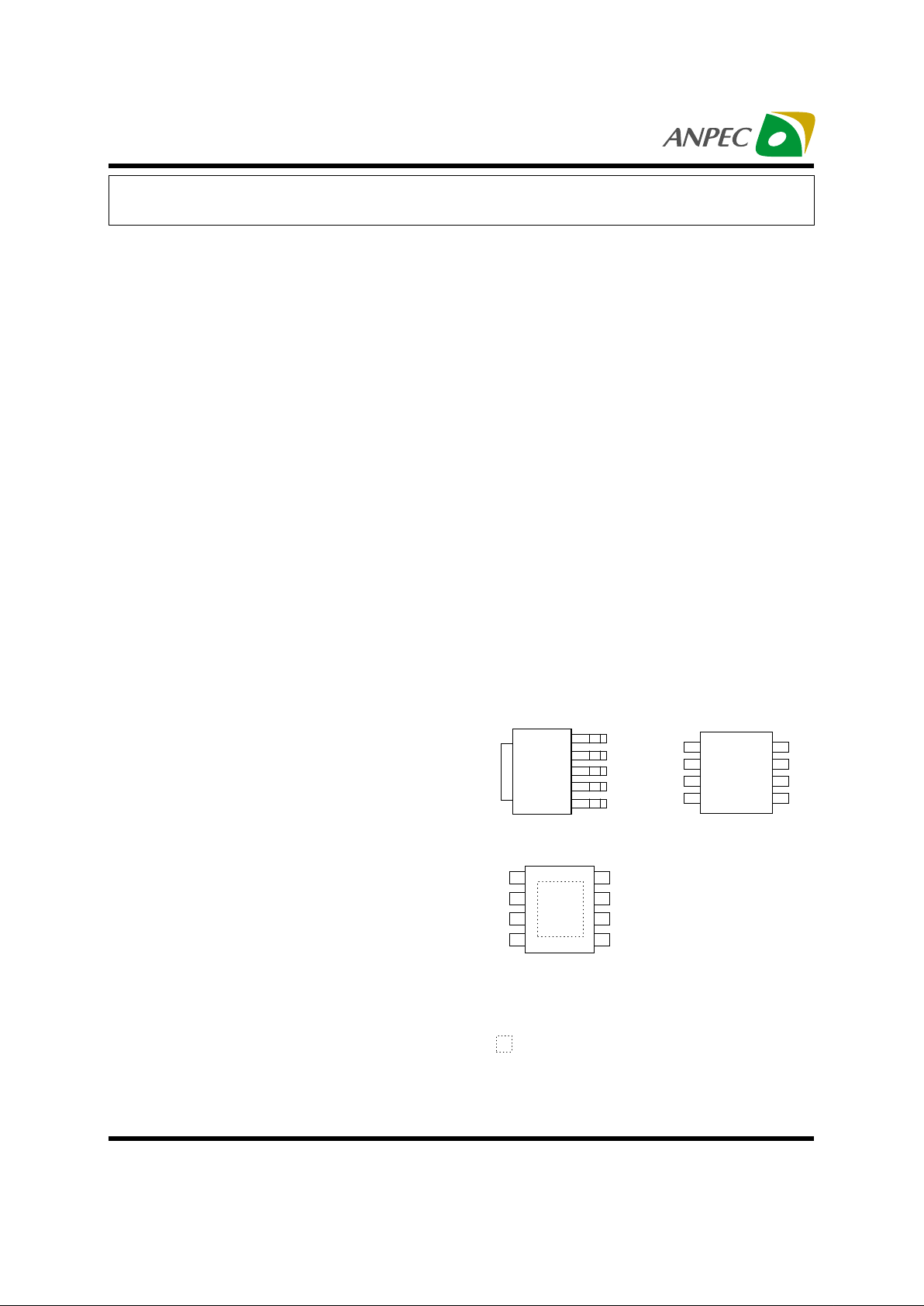
Pin Configuration
SO-8 (Top View)
1
2
3
45
6
7
8
VIN
BS
FB
VOUT GND
GND
GND
GND
TO-252-5 (Top View)
VOUT
FB
GND
BS
VIN
12345
TAB is GND
1
2
3
45
6
7
8
VIN
BS
FB
VOUT
NC
GND
NC
NC
SOP-8-P (Top View)
NC = No internal connection
= Thermal Pad
(connected to GND plane for better heat
dissipation)
Copyright ANPEC Electronics Corp.
Rev. A.3 - Oct., 2003
APL5332
www.anpec.com.tw2
Package Code
U5 : TO-252-5 K : SO -8 KA : SOP-8-P
Temp. Range
C : 0 to 70 C
Handling Code
TR : Tape & Reel
Lead Free Code
L : Lead Free Device Blank : Orginal Device
APL5332
Handling Code
Temp. Range
Package Code
APL5332
XXXXX
APL5332 K /KA :
XXXXX - Date Code
APL5332
XXXXX
APL5332 U :
XXXXX - Date Code
Lead Free Code
Ordering and Marking Information
°
Pin Function Description
PIN
No. Name
I/O Description
1 VIN I Input supply voltage.
2 BS I Fixed output voltage selection by this pin.
3 GND O Ground pin for signal ground and power ground.
4 FB I Adjust output voltage by this pin
5 VOUT O Regulator output voltage.
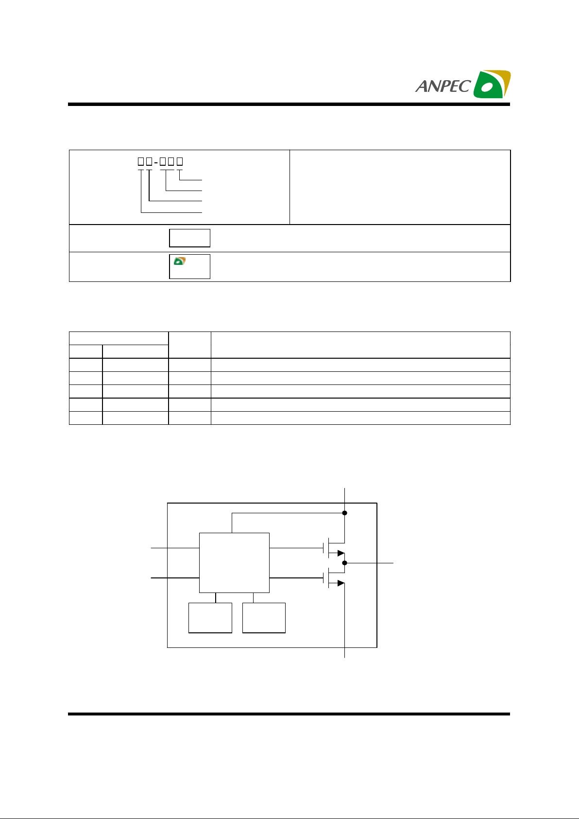
Block Diagram
C ontrol
Cir cuit
Curren t
Limit
Thermal
Contr ol
VIN
VOUT
FB
BS
GND
Copyright ANPEC Electronics Corp.
Rev. A.3 - Oct., 2003
APL5332
www.anpec.com.tw3
Symbol Parameter Rating Unit
VIN VIN Supply Voltage, VIN to GND -0.2 ~ 5.5 V
B S , F B to GN D -0.2 ~ VIN V
V
OUT
V OU T Ou t p u t Vo lta ge , VOU T to GN D -0 .2 ~ VIN V
PD Power Dissipation Internally Limited W
TJ Junction Temperature 150
o
C
T
STG
Storage Tem perature -65 ~ 150
o
C
T
SDR
S oldering Temperature, 10 Seconds 300
o
C
V
ESD
M inim um ES D R ating (Hum an Body Mode)
±
3
kV
Absolute Maximum Ratings
Thermal Characteristics
Symbol Parameter Value Unit
θ
JA
Junction-to-Ambient Thermal Resistance in Free Air
TO-252-5
SOP-8-P
SOP-8
80
80
150
o
C/W
Recommended Operating Conditions
Symbol Parameter Range Unit
VIN VIN Supply V oltage 2.4 ~ 3.5 V
I
OUT
VOUT Output Current (Note 1,2) -1 ~ +2 A
TJ Junction Temperature 0 ~ 125
o
C
Note 1 : The symbol “+” means the VOUT sources current to load; the symbol “-“ means the VOUT sinks
current to GND.
Note 2 : The max. IOUT varies with the TJ. Please refer to the typical characteristics.
Copyright ANPEC Electronics Corp.
Rev. A.3 - Oct., 2003
APL5332
www.anpec.com.tw4
Electrical Characteristics
Refer to the typical application circuit. These specifications apply over VIN=2.5~3.3V, and TJ= 0 to 125oC,
unless otherwise specified. Typical values refer to TJ =25oC.
APL5332
Symbol
Parameter Test Conditions
Min Typ Max
Unit
OUTPUT VOLTAGE
V
REF
Reference Voltage FB=VO U T
0.8
V
BS=VIN , FB=VIN
1.225
V
OUT
VOU T O utput Voltage
BS=GND, FB=VIN
1.45
V
I
OUT
=0A, TJ=25oC -1 +1
Accuracy
I
OUT
= -1~+2A, TJ=0~125oC -2 +2
%
I
OUT
=0A~+2A
VIN=2.5V
V
IN
=3.3V
0.5
1
Load Regulation
I
OUT
= 0~-1A
V
IN
=2.5V or 3.3V
0.7
%
Line Regulation I
OUT
=0A, VIN=2.5V ~ 3.3V
0.05
0.2 %
PROTECT ION
2.0
2.3
Sourcing Current TJ=25oC
(VIN=3.3V) TJ=125oC
1.7
1.2
1.7
Sinking Current TJ=25oC
(V
IN
=2.5V or 3.3V) TJ=125oC
1.3
A
1.7
2.0
I
LIM
Current Limit
Sourcing Current T
J
=25oC
(VIN=2.5V) TJ=125oC
1.5
A
TSD
Thermal Shutdown Tem perature Rising T
J
150
o
C
Thermal Shutdown Hysteresis 25
oC
BS AND FB THRESHOLD VOLTAGES
BSLogicHigh Threshold Voltage VBS Rising 0.6
0.8
1.0 V
BS Hysteresis
35
mV
BS Input Bias Current VIN=3 .3 V , BS= GN D -0 .1 7 -0.3
µA
FB Logic High Threshold Voltage
(VFB - V
IN)
V
FB
Rising -0.3 -0.46 -0.8 V
FB Hysteresis
35
mV
FB Input Bias Current V
IN
=3 .3 V , FB= 0 .8 V
-0.17
-0.3
µ
A
OTHER
IQ
Quiescent VIN Sup ply Current I
OUT
=0A 4
8
14 mA
V
POR
VIN Power-On-Reset Threshold
Voltage
1.4 2.1 2.4 V
TSS
So f t-S ta r t In te rv a l
1
mS
Copyright ANPEC Electronics Corp.
Rev. A.3 - Oct., 2003
APL5332
www.anpec.com.tw5
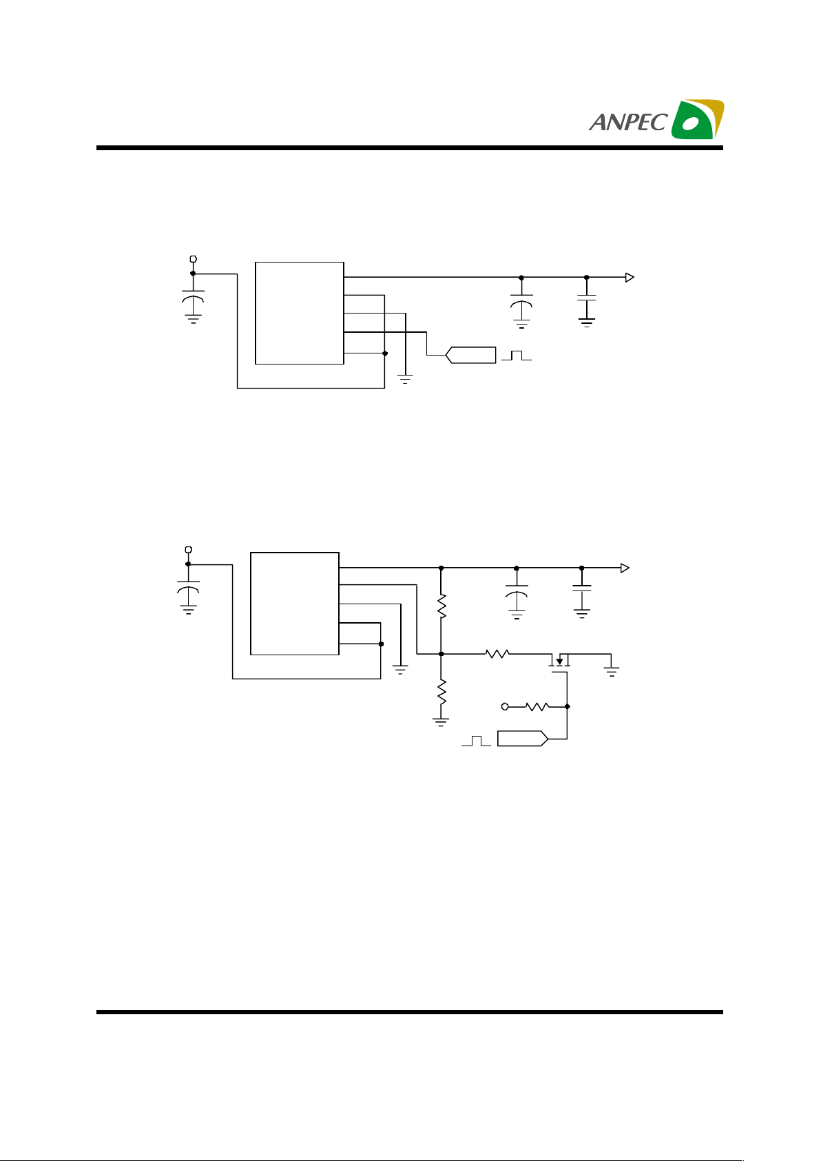
Typical Application Circuit
Typical Application For Processor MCH Power Selection Schematic
Use External Resistors to Select the Desired Output Voltage Schematic
VOUT
V
OUT
A PL5332
FB
GND
BS
VIN
5
4
3
2
1
BS=H, V
OUT
=1.225V
BS=L, V
OUT
=1.45V
BS
U1
+3.3V or +2.5V
V
IN
C1
47uF
C2
470uF
C3
1uF
VOUT
V
OUT
A PL5332
FB
GND
BS
VIN
5
4
3
2
1
BS(Inv)=H, V
OUT
=1.45V
BS(Inv)=L, V
OUT
=1.225V
BS(Inv)
+5V
R4
10K
Q1
A PM2300A
R3
3.02K
R2
1.6K
R1
850
U1
+3.3V or +2.5V
V
IN
C1
47uF
C2
470uF
C3
1uF
Copyright ANPEC Electronics Corp.
Rev. A.3 - Oct., 2003
APL5332
www.anpec.com.tw6
-3.0
-2.5
-2.0
-1.5
-1.0
-0.5
-50 -25 0 25 50 75 100 125
1.0
1.5
2.0
2.5
3.0
3.5
-50 -25 0 25 50 75 100 125
0.784
0.788
0.792
0.796
0.800
0.804
0.808
0.812
0.816
-50 -25 0 25 50 75 100 125
1.4
1.5
1.6
1.7
1.8
1.9
2.0
2.1
2.2
2.3
2.4
2.5
2.6
-50-25 0 255075100125
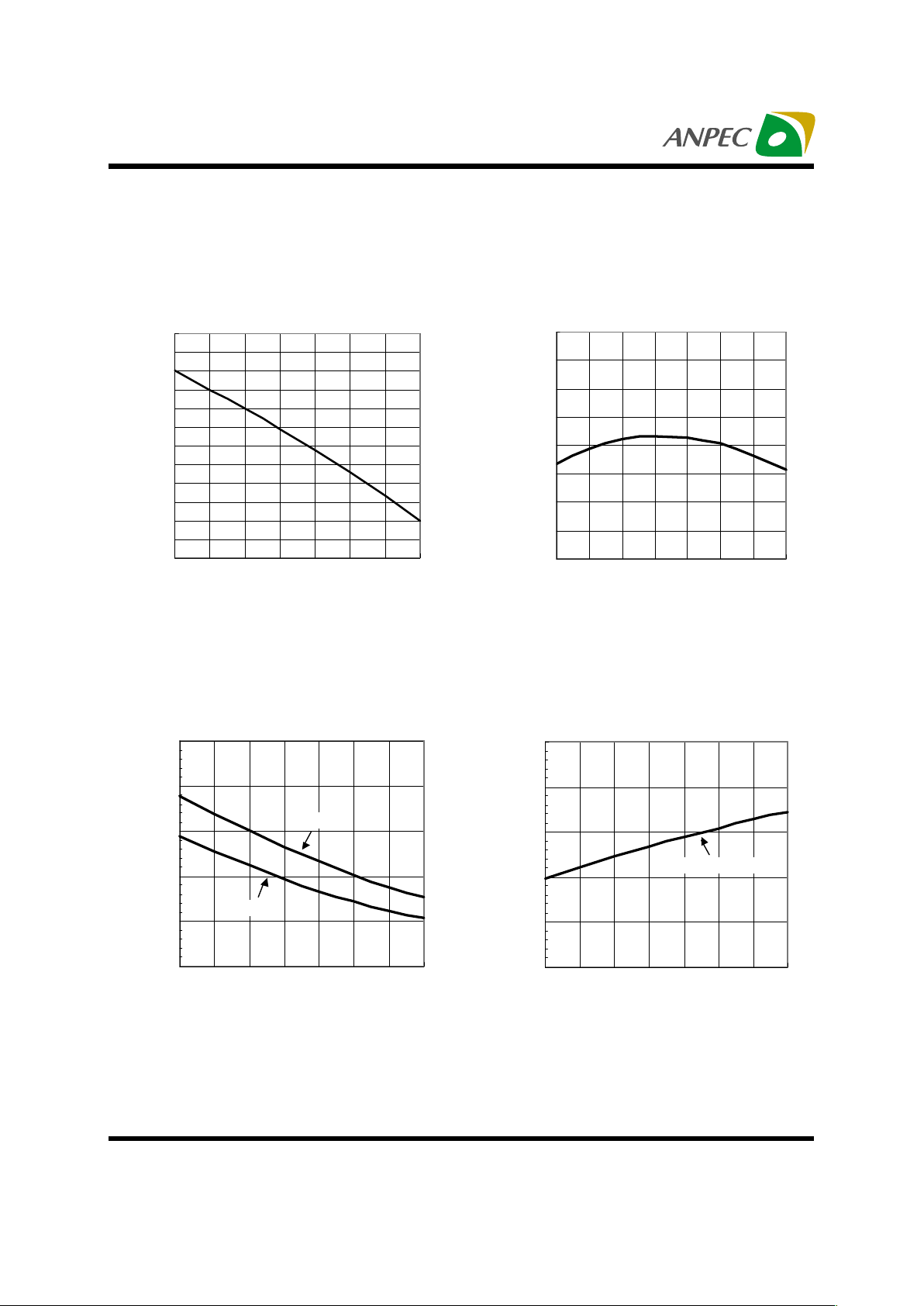
Typical Operating Characteristics
Power-On-Reset Threshold Voltage
vs Junction T emperature
Junction T emperature (oC)
Power-On-Reset Threshold Voltage (V)
VREF Shutdown Threshold
vs Junction T emperature
Junction T emperature (oC)
Reference Voltage, VREF (V)
Sourcing Current-Limit
vs Junction T emperature
Current-Limit, ILIM (A)
Junction T emperature (oC)
Sinking Current-Limit
vs Junction T emperature
Current-Limit, ILIM (A)
Junction T emperature (oC)
VIN = 2.5V or 3.3V
VIN = 3.3V
VIN = 2.5V

Copyright ANPEC Electronics Corp.
Rev. A.3 - Oct., 2003
APL5332
www.anpec.com.tw7
5.0
5.5
6.0
6.5
7.0
7.5
8.0
8.5
9.0
9.5
10.0
-50 -25 0 25 50 75 100 125
-0.8
-0.7
-0.6
-0.5
-0.4
-0.3
-0.2
-50-250 255075100125
0.5
0.6
0.7
0.8
0.9
1.0
1.1
-50 -25 0 25 50 75 100 125
Junction T emperature (°C)
Typical Operating Characteristics Cont.
BS Pin Threshold Voltage
vs Junction T emperature
BS Pin Threshold Voltage (V)
Junction T emperature (oC) Junction T emperature (oC)
FB Threshold Voltage
vs Junction T emperature
FB Threshold Voltage (V)
Quiescent VIN Current
vs Junction T emperature
Quiescent VIN Current (mA)
Rising
Falling
Rising
Falling
IOUT = 0A
VIN = 3.3V
VIN = 2.5V

Copyright ANPEC Electronics Corp.
Rev. A.3 - Oct., 2003
APL5332
www.anpec.com.tw8
Functional Description
General
APL5332 is a source-sink linear regulator designed
for motherboard front side bus. The device can supply
loads from -1A to 2A in either fixed or adjustable voltage mode. APL5332 has a 0.8V reference, an error
amplifier, two pass transistors, fixed voltage selection,
an internal feedback resistor-divider, soft-start control
and fault protections(current-limit and thermal
shutdown). The output voltage is either 1.225V or 1.
45V selected by the BS pin when fixed voltage mode
is active by setting FB=VIN. When the FB is connected with a feedback resistor-divider, the IC operates in adjustable voltage mode and the voltage of FB
is regulated to 0.8V. In the mode, the input of BS pin
is ignored. APL5332 is available in the SOP, SOP-8P, and TO-252-5 packages to meet different power
dissipation applications.
Output Voltage Regulation
The error amplifier working with the temperature-compensated 0.8V reference and the two pass transistors
(high-side and low-side) regulates the output to the
preset voltage. The error amplifier compares the reference with the feedback voltage and amplifies the difference to drive one of the pass transistors. The highside pass transistor provides current from VIN to VOUT
and increases the output voltage when the feedback
voltage is lower than the reference. The low-side pass
transistor provides current from VOUT to GND and decreases the output voltage when the feedback voltage is
higher than the reference. The two pass transistors are
well controlled by the error amplifier and prevented shortthrough conditions. An internal output voltage sense pad
is bonded to the VOUT pin for perfect load regulation in
fixed voltage mode.
Current Limit
The APL5332 monitors the sourcing or sinking currents and limits the maximum output current to prevent damages during overload or short-circuit
conditions.
Power-On-Reset and Soft-Start
A Power-On-Reset circuit monitors input voltage of
the VIN pin and prevents wrong logic controls. When
the input voltage rises up more than the Power-OnReset threshold voltage, the device starts to output
current. Therefore, a soft-start circuit which controls
the reference voltage to rise up is required, limiting
surge input currents. The typical soft-start interval is
about 1mS.
Thermal Shutdown
A thermal shutdown circuit limits the junction temperature of the APL5332. When the junction temperature exceeds +150oC, a thermal sensor turns off the
both pass transistors, allowing the device to cool
down. The regulator starts to regulate again after the
junction temperature cools by 25oC, resulting in a
pulsed output during continuous thermal overload
conditions. The thermal shutdown designed with a 25oC
hysteresis lowers the average junction temperature
during continuous thermal overload conditions, extending life time of APL5332.
For normal operation, device power dissipation should
be externally limited so that junction temperatures will
not exceed +125oC.

Copyright ANPEC Electronics Corp.
Rev. A.3 - Oct., 2003
APL5332
www.anpec.com.tw9
Application Information
Internal Parasitic Diode
Do not apply a voltage to VOUT when the voltage applied at VIN is not present. The reason is the internal
parasitic diodes from VOUT to VIN will conduct due to
the forward-voltage applied at VOUT.
Output Voltage Selection
The APL5332 allows operation in either fixed voltage
or adjustable mode. Connecting FB to VIN selects
fixed output voltage which is either 1.225V or 1.45V
by setting the BS pin to be logic “High” or “Low”. The
output voltage may also be adjusted by connecting a
resistor-divider from VOUT to FB to GND (See the
Typical Application Circuit). Selecting R2 in the 100Ω
to 5kΩ range ignors the voltage offset caused by the
internal pull-up current of FB. Calculate R1 with the
following equation:
R1 = R2 [(VOUT / VREF) - 1]
where VREF = 0.8V.
The output voltage selection table is :
Output Capacitor
The APL5332 requires a proper output capacitor to
maintain stability and improve transient response. The
output capacitor selection is dependent upon the ESR
(equivalent series resistance) and capacitance over
temperature and current ranges. The following chart
shows a stable region to select output capacitor for
APL5332. This region above the curve indicates minimum required ESR and capacitance to maintain
stability. However, the output capacitor should have
an ESR less than1Ω.
HL
H
1.225V 1.45V
L
Adjustable Adjustable
FB
BS
Ultra-low-ESR capacitors, such as ceramic chip
capacitors, may promote unstable or under-damped
transient response, but proper ceramic chip capacitors placed near loads can be used as decoupling
capacitors. A low-ESR solid tantalum and aluminum
electrolytic capacitor (ESR<1Ω) works extremely well
and provides good transient response and stability over
temperature.
0
20
40
60
80
100
10 100 1000
Capacitance(µF)
ESR (m
Ω
)
St able Region
0
20
40
60
80
100
10 100 1000
Capacitance(µF)
ESR (m
Ω
)
St able Region
The output capacitors are also used to reduce the slew
rate of load current and help the APL5332 to minimize
variations of the output voltage, improving transient
response. For this purpose, the low-ESR capacitors
are recommended.
Input Capacitor
The VIN input capacitor is not required for stability but
for supplying surge currents during large load transients,
preventing the input rail from dropping and improving
performance of APL5332. The parasitic inductors from
the voltage sources or other bulk capacitors to the
VIN pins will limit the slew rate of the surge currents
during large load transients, resulting in voltage drop
at VIN pin.
An aluminum electrolytic capacitor (>47µF) is recommended for VIN pin, and It is not necessary to use
low-ESR capacitors.

Copyright ANPEC Electronics Corp.
Rev. A.3 - Oct., 2003
APL5332
www.anpec.com.tw10
Application Information
Layout and Thermal Consideration
The input capacitors are normally placed near VIN for
good performances. Ceramic decoupling capacitors
for load must be placed as close to the load to reduce the parasitic inductors of traces. It is also recommended that the APL5332 and output capacitors
are placed near the load for good load regulation and
transient response. The negative pins of the input and
output capacitors and the GND pin of the APL5332
are connected to analog ground plane of the load.
See Figure 1. The SOP-8-P is a cost-effective package featuring a small size as a standard SOP-8 and
a bottom thermal pad to minimize the thermal resistance of the package, being applicable to high current applications. The thermal pad of SOP-8-P or TO252-5 is soldered to the top ground pad which is connected to the internal or bottom ground plane by several vias. The printed circuit board (PCB) forms a heat
sink and dissipates major heat into ambient air.
Thermal resistance consists of two main elements, θ
JC (junction-to-case thermal resistance) and θCA (case-
to-ambient thermal resistance). θJC is specified from
the IC junction to the bottom of the thermal pad directly below the die. θCA is the resistance from the
bottom of thermal pad to the ambient air and it in-
cludes
θCS (case-to-sink thermal resistance) and (sink-
to-ambient thermal resistance). The specified path for
heat flow is the lowest resistance path and it dissipates
major heat to the ambient air. Normally
θCA is major re-
sistance in the path. Enlarging the internal or bottom
ground plane reduces the resistance θCA . The relationship between power dissipation and temperatures is
PD = (TJ - TA) / θJA
where,
PD : power dissipation
TJ : Junction Temperature
TA : Ambient Temperature
θ JA : Junction-to-Ambient Thermal Resistance
Thermal pad
Die
Top
ground
pad
Printed
circuit
board
Internal
ground
plane
Vias
Ambient
Air
118 mil
102 mil
SOP-8-P
Figure 1
Figure 2 shows a recommended board layout using
the SOP-8-P package. An area of 140mil*110mil on
the top layer (250mil*250mil) is used as a thermal
pad for APL5332 and is connected to the internal or
bottom ground plane by vias. The vias shold have proper
hole size to retain solder, and help heat conduction.
More area of the internal or bottom plane reduces θJA
and is better for dissipating power. The recommended
area is without limit. Therefore the PCB and all components form a heat sink.
250mil
250m il
140m il
110mil
Internal or bottom
Ground plane
Top layer
ground plane
Soldering area
for bottom pad
Pad
Vias
1234
8
76 5
Figure 2

Copyright ANPEC Electronics Corp.
Rev. A.3 - Oct., 2003
APL5332
www.anpec.com.tw11
Figure 3 shows a board layout using the SOP-8-P
package. The demoboard is made of FR-4 material
and is a two-layer PCB. The board size and thickness
are 65mm* 65mm and 1.6mm. The copper thickness
of top and bottom layers is 2 oz. The partial layout
around APL5332 is as the details above and shown in
the figure 2. It uses 15mil vias to connect the top and
bottom ground plane. The θJA of the APL5332 (SOP-8P) mounted on the demodoard is about 41.3oC/W in
free air. Assuming the TA=25oC and the maximum
TJ=150oC (typical thermal limit temperature), the maximum power dissipation is calculated as :
PD(max) = (150 - 25) / 41.3
= 3.03W
If the TJ is designed to be below 125oC, the calculated
power dissipation should be less than :
PD = (125 - 25) / 41.3
= 2.42W
Application Information
Figure 3(b) T op layer
Figure 3(c) Bottom layer
Figure 3(a) T opOver layer
APL5332
APL5332

Copyright ANPEC Electronics Corp.
Rev. A.3 - Oct., 2003
APL5332
www.anpec.com.tw12
Packaging Information
TO-252-5
Millim e te rs Inche s
Dim
Min. Max. Min. Max.
A 6.40 6.80 0.25 0.2 6
B 5.20 5.50 0.20 0.2 1
C 6 .8 0 7.2 0 0.26 0.2 7
D 2 .2 0 2.8 0 0.08 0.11
P 1.27 R E F 0.05 REF
S 0.50 0.80 0.02 0.0 3
H 2 .2 0 2.4 0 0.08 0.0 9
J 0.45 0.55 0.01 0.0 2
K 0 0.15 0 0.006
L 0 .9 0 1.50 0.0 3 0.0 6
M 5.40 5.80 0.2 1 0.2 2
L
K
J
H
B
A
C
M
D
PS

Copyright ANPEC Electronics Corp.
Rev. A.3 - Oct., 2003
APL5332
www.anpec.com.tw13
Packaging Information
Millimeters Inches
Dim
Min. Max. Min. Max.
A 1.35 1.75 0.053 0.069
A1 0.10 0.25 0.004 0.010
D 4.80 5.00 0.189 0.197
E 3.80 4.00 0.150 0.157
H 5.80 6.20 0.228 0.244
L 0.40 1.27 0.016 0.050
e1 0.33 0.51 0.013 0.020
e2 1.27BSC 0.50BSC
φ 1 8° 8°
HE
e1 e2
0.015X45
D
A
A1
0.004max.
1
L
SOP-8 pin ( Reference JEDEC Registration MS-012)

Copyright ANPEC Electronics Corp.
Rev. A.3 - Oct., 2003
APL5332
www.anpec.com.tw14
Packaging Information
SOP-8-P pin ( Reference JEDEC Registration MS-012)
HE
e1 e2
0.015X45
D
A
A1
0.004max.
1
L
E1
D1
Millimeters Inches
Dim
Min. Max. Min. Max.
A 1.35 1.7 5 0.0 53 0.0 69
A1 0.10 0.25 0.004 0.010
D 4.80 5.00 0.189 0.197
D1
3.00REF
0.118REF
E 3.80 4.0 0 0.1 50 0.1 57
E1 2.60REF 0.1 02REF
H 5.80 6.20 0.228 0.244
L 0.40 1.27 0.016 0.050
e1 0.33 0.51 0.013 0.020
e2 1.27BSC 0.50BSC
φ 18° 8°

Copyright ANPEC Electronics Corp.
Rev. A.3 - Oct., 2003
APL5332
www.anpec.com.tw15
Physical Specifications
Reference JEDEC Standard J-STD-020A APRIL 1999
Reflow Condition (IR/Convection or VPR Reflow)
Pre-heat temperature
183 C
Peak temperature
Time
°
temperature
Classification Reflow Profiles
Convection or IR/
Convection
VPR
Average ramp-up rate(183°C to Peak) 3°C/second max. 10 °C /second max .
Preheat temperature 125 ± 25°C)
120 seconds max
Temperature maintained above 183°C
60 – 150 seconds
Time within 5°C of actual peak temperature
10 –20 seconds 60 seconds
Peak temperature range
220 +5/-0°C or 235 +5/-0°C 215-219°C or 235 +5/-0°C
Ramp-down rate
6 °C /second max. 10 °C /second max .
Time 25°C to peak temperature
6 minutes max.
Package Reflow Conditions
pkg. thickness
≥≥≥≥
2.5mm
and all bgas
pkg. thickness < 2.5mm and
pkg. volume
≥≥≥≥
350 mm³
pkg. thickness < 2.5mm and pkg.
volume < 350mm³
Convection 220 +5/-0 °C Convection 235 +5/-0 °C
VPR 215-219 °C VPR 235 +5/-0 °C
IR/Convection 220 +5/-0 °C IR/Convection 235 +5/-0 °C
Terminal Material Solder-Plated Copper (Solder M ater ial : 90/10 or 6 3/3 7 S n Pb)
Lead Solderab ility Meets EIA Specification RSI86-91, A NSI/J-STD-002 Category 3.

Copyright ANPEC Electronics Corp.
Rev. A.3 - Oct., 2003
APL5332
www.anpec.com.tw16
R e lia bilit y te s t p r o g r a m
Test item M ethod Description
SOLDERABILITY M IL-STD-883D-2003
245°C , 5 SEC
HO LT MIL-STD-883D-1005.7
1000 Hrs Bias @ 125 °C
PCT JESD-22-B, A102
168 Hrs, 100 % RH , 121°C
TST MIL-STD-883D-1011.9
-65°C ~ 150°C, 200 Cycles
ESD MIL-STD-883D-3015.7 VHBM > 2KV, VM M > 200V
La tc h -Up JE SD 7 8 10 ms , Itr > 100mA
Carrier Tape
A
J
B
T2
T1
C
t
Ao
E
W
Po
P
Ko
Bo
D1
D
F
P1

Copyright ANPEC Electronics Corp.
Rev. A.3 - Oct., 2003
APL5332
www.anpec.com.tw17
Application Carrier Width Cover Tape Width Devices Per Reel
TO- 252
16 13.3 2500
SOP- 8
12 9.3 2500
SOT- 89
12 9.3 1000
Application
A B C J T1 T2 W P E
330 ±3100 ± 213 ± 0. 5 2 ± 0.5
16.4 + 0.3
-0.2
2.5± 0.5
16+ 0.3
- 0.1
8 ± 0.1 1.75± 0.1
F D D1 Po P1 Ao Bo Ko t
TO-252
7.5 ± 0.1 1.5 +0.1 1.5± 0.25 4.0 ± 0.1 2.0 ± 0.1 6.8 ± 0.1 10.4± 0.1 2.5± 0.1 0.3±0.05
Application
A B C J T1 T2 W P E
330 ± 1 62 +1.5
12.75+
0.15
2 ± 0.5 12.4 ± 0.2 2 ± 0.2 12± 0. 3 8± 0.1 1.75±0.1
F D D1 Po P1 Ao Bo Ko t
SOP- 8
5.5± 1 1.55 +0.1 1.55+ 0.25 4.0 ± 0.1 2.0 ± 0.1 6.4 ± 0.1 5.2± 0. 1 2.1± 0.1 0.3±0.013
Application
A B C J T1 T2 W P E
178 ±170 ± 213.5 ± 0.15 3 ± 0.15 14 ± 2 1.3 ± 0.3
12 + 0.3
12 - 0.1
8 ± 0.1 1.75± 0.1
F D D1 Po P1 Ao Bo Ko t
SOT-89
5.5 ± 0.05 1.5± 0.1 1.5± 0.1 4.0 ± 0.1 2.0 ± 0.1 4.8 ± 0.1 4.5± 0.1 1.80± 0.1 0.3±0.013
Cover Tape Dimensions
Anpec Electronics Corp.
Head Office :
5F, No. 2 Li-Hsin Road, SBIP,
Hsin-Chu, T aiwan, R.O.C.
T el : 886-3-5642000
Fax : 886-3-5642050
Taipei Branch :
7F, No. 137, Lane 235, Pac Chiao Rd.,
Hsin Tien City, Taipei Hsien, Taiwan, R. O. C.
T el : 886-2-89191368
Fax : 886-2-89191369
Customer Service
 Loading...