

Page 1
APL5325
Adjustable Low Dropout 300mA Linear Regulator
Features
• Wide Operating Voltage: 3~6V
• Low Dropout Voltage:
300mV(Typical) @ 300mA
• Guaranteed 300mA Output Current
• Adjustable Output Voltage: 0.8~5.5V
• Current-Limit Protection with Foldback Current
• Over-Temperature Protection
• Stable with Low ESR Ceramic Capacitor
• SOT-23-5 Package
• Lead Free and Green Devices Available
(RoHS Compliant)
Applications
• Cellular Phones
• Portable and Battery-Powered Equipment
General Description
The APL5325 is a P-channel low dropout linear regulator
which needs only one input voltage from 3 to 6V, and
delivers current up to 300mA to set output voltage. It also
can work with low ESR ceramic capacitors and is ideal for
using in the battery-powered applications such as notebook computers and cellular phones. Typical dropout voltage is only 300mV at 300mA loading.
Current limit with current foldback and thermal shutdown
functions protect the device against c urrent over-loads
and over temperature. The APL5325 is available in a SOT23-5 package.
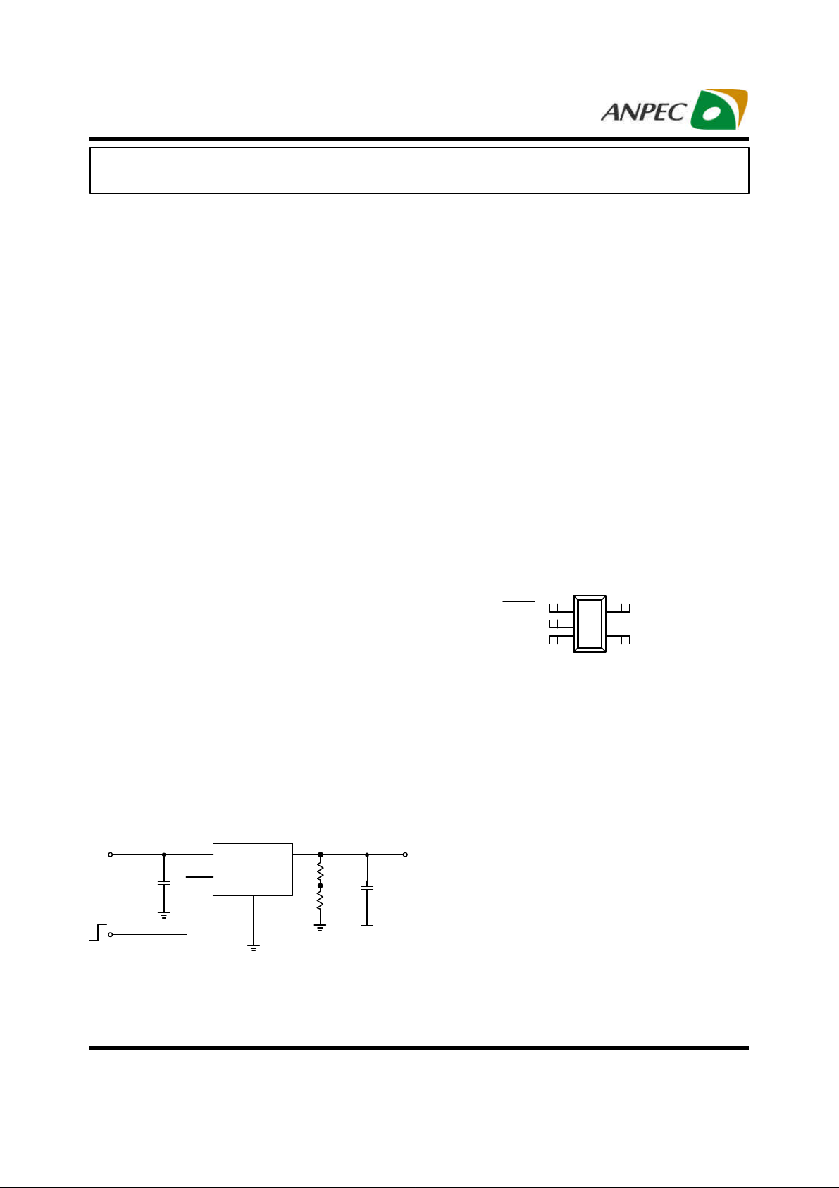
Pin Configuration
SHDN 1
GND 2
VIN 3
SOT-23-5
5 SET
4 VOUT
• Notebook and Personal Computers
Simplified Application Circuit
V
IN
C
IN
ANPEC reserves the right to make changes to improve reliability or manufacturability without notice, and
advise customers to obtain the latest version of relevant information to verify before placing orders.
Copyright ANPEC Electronics Corp.
Rev. A.1 - Nov., 2008
3
1
APL5325
VIN
SHDN
GND
2
VOUT
SET
4
5
V
OUT
C
OUT
www.anpec.com.tw1
Page 2
APL5325
Ordering and Marking Information
APL5325
Assembly Material
Handling Code
Temperature Range
Package Code
Package Code
B: SOT-23-5
Operating Ambient Temperature Range
I : -40 to 85 oC
Handling Code
TR : Tape & Reel
Assembly Material
L : Lead Free Device
G : Halogen and Lead Free Device
APL5325 B :
25RX XXXXXX - Date Code
Note: ANPEC lead-free products contain molding compounds/die attach materials and 100% matte tin plate termination finish; which
are fully compliant with RoHS. ANPEC lead-free products meet or exceed the lead-free requirements of IPC/JEDEC J-STD-020C for
MSL classification at lead-free peak reflow temperature. ANPEC defines “Green” to mean lead-free (RoHS compliant) and halogen
free (Br or Cl does not exceed 900ppm by weight in homogeneous material and total of Br and Cl does not exceed 1500ppm by
weight).
Absolute Maximum Ratings (Note 1)
Symbol Parameter Rating Unit
V
IN
V
SHDN
P
D
T
J
T
STG
T
SDR
Note 1: Absolute Maximum Ratings are those values beyond which the life of a device may be impaired. Exposure to absolute
maximum rating conditions for extended periods may affect device reliability.
VIN Supply Voltage (VIN to GND) -0.3 ~ 6.5 V
SHDN Input Voltage (SHDN to GND) -0.3 ~ 6.5 V
Power Dissipation Internally Limited W
Junction Temperature -40 ~ 150
Storage Temperature -65 ~ 150
Maximum Lead Soldering Temperature, 10 Seconds 260
o
C
o
C
o
C
Thermal Characteristics
Symbol Parameter Typical Value Unit
θJA
θJC
Thermal Resistance-Junction to Ambient
Thermal Resistance-Junction to Case
Note 2 : θJA is measured with the component mounted on a high effective thermal conductivity test board in free air.
(Note 2)
SOT-23-5
SOT-23-5
240
130
Recommended Operating Conditions
Symbol Parameter Range Unit
VIN VIN Supply Voltage 3 ~ 6 V
V
Output Voltage 0.8 ~ 5.5 V
OUT
I
VOUT Output Current 0 ~ 300 mA
OUT
CIN Input Capacitor 0.22 ~ 100
C
Output Capacitor 1.5 ~ 100
OUT
TJ Junction Temperature -40 ~ 125
Copyright ANPEC Electronics Corp.
Rev. A.1 - Nov., 2008
www.anpec.com.tw2
o
C/W
o
C/W
µF
µF
o
C
Page 3
APL5325
Electrical Characteristics
Unless otherwise specified, these specifications apply over VIN = V
Typical values are at TA = 25oC.
OUT
+1V, I
=0~300mA, CIN = 1µF, C
OUT
= 2.2µF, TA = -40 to 85oC.
OUT
Symbol
Parameter Test Conditions
APL5325
Min. Typ. Max.
VIN Input Voltage 3 - 6 V
V
Output Voltage Range 0.8 - 5.5 V
OUT
IQ Quiescent Current I
V
Reference Voltage Measured on SET, VIN=3V, I
REF
Output Voltage Accuracy I
REG
REG
V
LINE
LOAD
DROP
Line Regulation
Load Regulation
Dropout Voltage
PSRR Power Supply Ripple Rejection Ratio f = 10kHz, I
Noise f = 80Hz to 100kHz, I
I
Current Limit 450 550 - mA
LIMIT
I
SHORT
Foldback Current V
=10mA ~300mA - 135 160
OUT
=10mA
OUT
=10mA -2 - +2 %
OUT
∆V
%/∆VIN, I
OUT
∆V
%/∆I
OUT
V
= 2.5V, I
OUT
V
= 3.3V, I
OUT
= 0V - 80 - mA
OUT
=10mA
OUT
OUT
= 300mA - 500 650
OUT
= 300mA - 300 400
OUT
= 300mA - 45 - dB
OUT
= 300mA - 160 -
OUT
- 0.8 - V
-0.06
- +0.06 %/V
-0.2 - +0.2 %/A
SHDN Input Voltage High 1.6 - SHDN Input Voltage Low
- - 0.4
Unit
µA
mV
µV
RMS
V
V
Shutdown VIN Supply Current SHDN = Low, V
Discharge MOSFET R
OUT
SHDN = Low - 60 -
DS(ON)
= 6V - 0.1 1
IN
SHDN Pull Low Resistance - 3 Over Temperature Threshold - 160 -
Over Temperature Hysteresis
SET Input Bias Current
- 40 V
=0.8V -100 - 100 nA
SET
Copyright ANPEC Electronics Corp.
Rev. A.1 - Nov., 2008
Ω
µA
MΩ
o
C
o
C
www.anpec.com.tw3
Page 4
APL5325
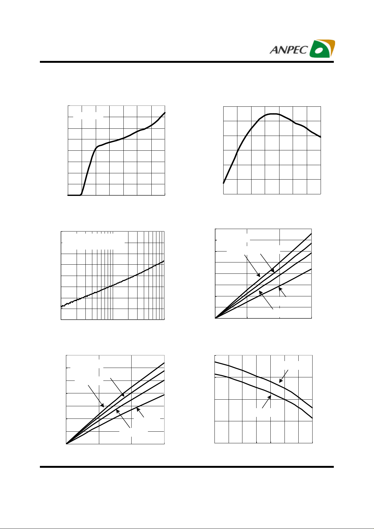
Typical Operating Characteristics
Quiescent Current vs. Supply Voltage Quiescent Current vs. Junction Temperature
160
I
OUT
= 0mV
(µA)
140
120
Q
100
138
136
(µA)
Q
134
80
60
40
Quiescent Current, I
20
0
0 1 2 3 4 5 6 7
Supply Voltage, VIN (V)
PSRR vs. Frequency
0
VIN=3.3V, V
-10
C
=2.2µF,I
OUT
-20
-30
-40
-50
PSRR(dB)
-60
-70
-80
1000 10000 100000
=1.2V,
OUT
=300mA
OUT
Frequency(Hz)
132
130
Quiescent Current, I
128
126
-50 -25 0 25 50 75 100 125
Junction Temperature, TJ (oC)
Dropout Voltage vs. Output Current
400
V
=3.3V
350
(mV)
300
DROP
250
200
150
100
Dropout Voltage, V
OUT
TJ=125oC
TJ=75oC
50
TJ=25oC
0
0 100 200 300
Output Current, I
OUT
TJ=-50oC
(mA)
Dropout Voltage vs. Output Current
700
V
=2.5V
600
(mV)
500
DROP
400
300
200
Dropout Voltage, V
100
Copyright ANPEC Electronics Corp.
Rev. A.1 - Nov., 2008
OUT
TJ=75oC
TJ=125oC
TJ=25oC
0
0 100 200 300
Output Current, I
OUT
TJ=-50oC
(mA)
Current Limit vs. Junction Temperature
600
VIN=5V
550
(mA)
LIMIT
500
VIN=3.3V
450
Current Limit, I
400
-50 -25 0 25 50 75 100 125
Junction Temperature, TJ(oC)
www.anpec.com.tw4
Page 5
APL5325
Typical Operating Characteristics (Cont.)
Loop Gain vs. Frequency
50
40
30
20
10
0
-10
Loop Gain (dB)
-20
-30
-40
VIN=3.3V, V
CIN=1µF, C
I
=300mA
OUT
OUT
OUT
=1.2V,
=2.2µF
I
OUT
1000 10000 100000 1000000
Frequency (Hz)
=100mA
Phase vs. Frequency
160
140
120
100
80
60
Phase (degree)
40
20
0
VIN=3.3V, V
CIN=1µF, C
I
OUT
OUT
OUT
=1.2V,
=2.2µF
=100mA
I
OUT
=300mA
1000 10000 100000 1000000
Frequency (Hz)
Copyright ANPEC Electronics Corp.
Rev. A.1 - Nov., 2008
www.anpec.com.tw5
Page 6

APL5325
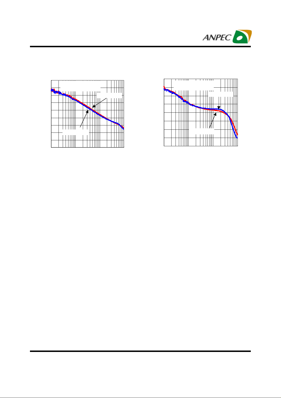
Operating Waveforms
Enable Shutdown
SHDN
CH1
V
IN
CH2
V
I
OUT
OUT
CH3
CH4
CH1 : SHDN , 5V/div
CH2 : VIN , 5V/div
CH3 : V
CH4 : I
OUT
Time : 200µs/div
VIN=5V ; C
C
=2.2µF ; TR=1µs
OUT
CH1
CH1
CH2
CH3
CH4
CH1 : SHDN , 5V/div
CH2 : VIN , 5V/div
, 2V/div
OUT
, 100mA/div
CH3 : V
CH4 : I
Time : 10µs/div
, 2V/div
OUT
, 100mA/div
OUT
Load Transient Line Transient
=1µF ;
I N
CIN=1µF ; C
V
OUT
TR=5µs ; I
V
IN
OUT
=2.2µF ;
OUT
=10mA
SHDN
V
IN
V
OUT
I
OUT
I
OUT
CH2
CH1 : V
CH2 : I
Time : 20µs/div
, 50mV/div AC
OUT
, 100mA/div
OUT
Copyright ANPEC Electronics Corp.
Rev. A.1 - Nov., 2008
V
OUT
CH2
CH1
CH1 : VIN , 1V/div DC
CH2 : V
Time : 20µs/div
, 50mV/div AC
OUT
www.anpec.com.tw6
Page 7

APL5325
Operating Waveforms (Cont.)
Power On
V
CH1
CH2
CH3
CH1 : VIN , 2V/div
CH2 : V
CH3 : I
Time : 2ms/div
IN
V
OUT
I
OUT
, 2V/div
OUT
, 100mA/div
OUT
CH1
CH2
CH3
Pin Description
PIN
NO. NAME
1 SHDN Shutdown control pin, logic high: enable; logic low: shutdown.
2 GND Ground pin.
3 VIN Voltage supply input pin.
4 VOUT Regulator output pin.
5 SET
Connect this pin to an external resistor divider to adjust output voltage.
FUNCTION
CH1 : VIN , 2V/div
CH2 : V
CH3 : I
, 2V/div
OUT
, 100mA/div
OUT
Time : 10ms/div
Power Off
V
IN
V
OUT
I
OUT
Copyright ANPEC Electronics Corp.
Rev. A.1 - Nov., 2008
www.anpec.com.tw7
Page 8

APL5325
Block Diagram
SHDN
Thermal
Shutdown
3MΩ
GND
Typical Application Circuit
UVLO &
Shutdown
Logic
0.8V
VIN
-
+
Foldback
Current
Limit
VOUT
SET
V
IN
C
IN
1µF
Enable
Shutdown
Designation Supplier
CIN Murata GRM185R61A105KE36
CIN Murata GRM188R71A105KA61
C
Murata GRM188R61A225KE34
OUT
C
Murata GRM188R71A225KE15
OUT
Reference: www.murata.com
Copyright ANPEC Electronics Corp.
Rev. A.1 - Nov., 2008
3 4
VIN
1
SHDN
OUT
VOUT
SET
GND
2
R1
+⋅=
10.8 V
R2
Part Number Specification
5
R
1
R
2
0603, X5R, 10V, 1µF
0603, X7R, 10V, 1µF
0603, X5R, 10V, 2.2µF
0603, X7R, 10V, 2.2µF
V
C
OUT
2.2µF
OUT
www.anpec.com.tw8
Page 9

APL5325
Function Description
Output Voltage Regulation
The APL5325 is an adjustable low dropout linear
regulator. The output voltage set by the resistor-divider is
determined by:
R1
OUT
Where R1 is connec ted from VOUT to SET with Kelvin
sensing and R2 is connected from SET to GND. The recommended value of R2 is in the range of 100 to100kΩ.
An error amplifier works with a temperature compensated
0.8V reference and an output PM OS regulates the output
to the presetting voltage. The error amplifier is designed
with high bandwidth and DC gain provides very fast transient response and less load regulation. It compares the
reference with the feedback voltage and amplifies the difference to drive the output PMOS which provides load
current from VIN to VOUT.
+⋅=
10.8 V
R2
Thermal Shutdown
A thermal shutdown c ircuit limits the junction temperature of APL5325. When the junction temperature exceeds
+160οC, a thermal sensor turns off the output PMOS, allowing the device to cool down. The regulator regulates
the output again through initiation of a new soft-start cycle
after the junction temperature is c ooled down by 40oC.
The thermal shutdown is designed with a 40oC hysteresis to lower the av erage junction temperature during
continuous thermal overload c onditions, extending lifetime of the device.
For normal operation, device power diss ipation should
be externally limited so that junction temperature will not
exceed 125oC.
Shutdown Control
The APL5325 has an active-low shutdown function. Force
SHDN high (>1.6V) enables the V
(<0.4V) disables the V
. SHDN is internally pulled low
OUT
; force SHDN low
OUT
by a resistor (3mΩ typical). If it is not used, connect to VIN
for normal operation.
Copyright ANPEC Electronics Corp.
Rev. A.1 - Nov., 2008
www.anpec.com.tw9
Page 10

APL5325
Application Information
Input Capacitor
The APL5325 requires proper input capacitors to supply
surge c urrent during stepping load transients to prevent
the input rail from dropping . Because the parasitic inductor from the voltage sources or other bulk capacitors to
the VIN limit the slew rate of the surge current, place the
Input capacitors near VIN as close as possible. Input capacitors should be larger than 1µF and a minimum ceramic capacitor of 1µF is necess ary.
Output Capacitor
The APL5325 needs a proper output capacitor to maintain circuit stability and to improve transient response over
temperature and current. In order to insure the circuit
stability, the proper output capacitor value should be larger
than 2.2µF. With X5R and X7R dielectrics, 2.2µF is sufficient at all operating temperatures. Large output capacitor value can reduce noise and improve load-transient
respons e and PSRR, however, it also affects power on
issue. Equation (1) shows the relationship between the
maximum C
OUT(max)
Where the unit of C
value and the V
OUT
19.5
101C −=
V
OUT
is µF and V
OUT
.
OUT
is V. Figure 1 shows
OUT
the curve of maximum output capacitor over the output
voltage. The output voltage range is from 0.8 to 5.5V and
the output capacitor value should under the line. Output
capacitors must be placed at the load and the ground pin
as c lose as possible and the impedance of the layout
must be minimized.
120
110
F)
100
90
Operation Region and Power Dissipation
The APL5325 maximum power dissipation depends on
the thermal resistance and temperature difference between the die junction and ambient air. The power dissipation PD across the device is:
PD = (TJ - TA) / θ
JA
where (TJ-TA) is the temperature difference between the
junction and ambient air. θJA is the thermal resistance
between Junction and ambient air. Ass uming the
TA=25oC and maximum TJ=160oC (typical thermal limit
threshold), the maximum power dissipation is calculated as:
P
=(160-25)/240
D(max)
= 0.56(W)
For normal operation, do not exceed the maximum junction temperature rating of TJ = 125 oC. The calculated power
diss ipation should less than:
PD =(125-25)/240
= 0.41(W)
The GND provides an electrical connection to the ground
and channels heat away. Connect the GND to the ground
by using a large pad or a ground plane.
Layout Consideration
Figure 2 illustrates the layout. Below is a check list for
your layout:
1. Please place the input capacitors close to the VIN.
2. Ceramic c apacitors for load must be placed near the
load as clos e as possible.
3. To place APL5325 and output capacitors near the load
is good for performance.
4. Large current paths, the bold lines in figure 2, must
have wide tracks.
5. Divider resistor R1 and R2 must be placed near the
SET as c lose as possible.
80
70
Output Capacitor (µ
60
0 1 2 3 4 5 6
Output Voltage (V)
Figure 1
Copyright ANPEC Electronics Corp.
Rev. A.1 - Nov., 2008
www.anpec.com.tw10
Page 11

APL5325
Application Information (Cont.)
Layout Consideration (Cont.)
C
IN
APL5325
VOUT
GND
2
VIN
SET
3
4
5
R
1
R
2
Figure 2
Recommended Minimum Footprint
SOT-23-5
V
IN
V
OUT
C
OUT
LOAD
0.076
0.1
0.05
0.038
0.02
Unit : Inch
Copyright ANPEC Electronics Corp.
Rev. A.1 - Nov., 2008
www.anpec.com.tw11
Page 12

APL5325
Pack age Information
SOT-23-5
D
e
b c
e1
SEE
VIEW A
E1
E
A
A2A1
L
VIEW A
0.25
GAUGE PLANE
SEATING PLANE
0
MAX.
0.15
0.50
0.22
3.00
1.80
0.60
8
SOT-23-5
MIN.
0.000
0.035
0.003
0.106
0.055
0.012
0
INCHES
MAX.
0.057
0.006
0.051
0.0200.012
0.009
0.122
0.1180.102
0.071
0.037 BSC
0.075 BSC
0.024
8
S
Y
M
B
O
L
A
A1
A2
b
c
D
E
E1
e
e1
L
0
Note : 1. Follow JEDEC TO-178 AA.
2. Dimension D and E1 do not include mold flash, protrusions or gate
burrs. Mold flash, protrusion or gate burrs shall not exceed 10 mil
per side.
MILLIMETERS
MIN.
0.00
0.90
0.30
0.08
2.70
2.60
1.40
0.95 BSC
1.90 BSC
0.30
0
1.45
1.30
3.10
Copyright ANPEC Electronics Corp.
Rev. A.1 - Nov., 2008
www.anpec.com.tw12
Page 13

APL5325
Carrier Tape & R eel Dimensions
OD0
B0
P0
P2
P1
A
E1
F
W
Application
SOT-23-5
K0
SECTION A-A
B
A
H
A0
SECTION B-B
OD1
B
T
A
d
T1
A H T1 C d D W E1 F
178.0±2.00 50 MIN.
8.4+2.00
-0.00
13.0+0.50
-0.20
1.5 MIN. 20.2 MIN. 8.0±0.30 1.75±0.10 3.5±0.05
P0 P1 P2 D0 D1 T A0 B0 K0
4.0±0.10 4.0±0.10 2.0±0.05
1.5+0.10
-0.00
1.0 MIN.
0.6+0.00
-0.40
3.20±0.20 3.10±0.20 1.50±0.20
(mm)
Devices Per Unit
Package Type Unit Quantity
SOT-23-5
Copyright ANPEC Electronics Corp.
Rev. A.1 - Nov., 2008
Tape & Reel 3000
www.anpec.com.tw13
Page 14

APL5325
Taping Direction Information
SOT-23-5
USER DIRECTION OF FEED
Reflow Condition (IR/Convection or VPR Reflow)
T
P
Ramp-up
T
L
Tsmax
Tsmin
Temperature
ts
Preheat
25
°
t 25 C to Peak
tp
t
L
Ramp-down
Critical Zone
TL to T
Time
Reliability Test Program
Test item Method Description
SOLDERABILITY MIL-STD-883D-2003
HOLT MIL-STD-883D-1005.7
PCT JESD-22-B, A102
TST MIL-STD-883D-1011.9
ESD MIL-STD-883D-3015.7 VHBM > 2KV, VMM > 200V
Latch-Up JESD 78 10ms, 1tr > 100mA
245°C, 5 sec
1000 Hrs Bias @125°C
168 Hrs, 100%RH, 121°C
-65°C~150°C, 200 Cycles
P
Copyright ANPEC Electronics Corp.
Rev. A.1 - Nov., 2008
www.anpec.com.tw14
Page 15

APL5325
Classification Reflow Profiles
Profile Feature Sn-Pb Eutectic Assembly Pb-Free Assembly
Average ramp-up rate
(TL to TP)
Preheat
- Temperature Min (Tsmin)
- Temperature Max (Tsmax)
- Time (min to max) (ts)
Time maintained above:
- Temperature (TL)
- Time (tL)
Peak/Classification Temperature (Tp)
Time within 5°C of actual
Peak Temperature (tp)
Ramp-down Rate
Time 25°C to Peak Temperature
Note: All temperatures refer to topside of the package. Measured on the body surface.
Table 1. SnPb Eutectic Process – Package Peak Reflow Temperatures
Package Thickness
<2.5 mm
≥2.5 mm 225 +0/-5°C 225 +0/-5°C
Table 2. Pb-free Process – Package Classification Reflow Temperatures
Package Thickness
<1.6 mm
1.6 mm – 2.5 mm
≥2.5 mm 250 +0°C* 245 +0°C* 245 +0°C*
* Tolerance: The device manufacturer/supplier shall assure process compatibility up to and including the stated
classification temperature (this means Peak reflow temperature +0°C. For example 260°C+0°C) at the rated MSL
level.
Volume mm3
<350
260 +0°C* 260 +0°C* 260 +0°C*
260 +0°C* 250 +0°C* 245 +0°C*
3°C/second max. 3°C/second max.
100°C
150°C
60-120 seconds
183°C
60-150 seconds
See table 1 See table 2
10-30 seconds 20-40 seconds
6°C/second max. 6°C/second max.
6 minutes max. 8 minutes max.
Volume mm
<350
240 +0/-5°C 225 +0/-5°C
3
Volume mm3
350-2000
150°C
200°C
60-180 seconds
217°C
60-150 seconds
Volume mm
≥350
Volume mm3
3
>2000
Customer Service
Anpec Electronics Corp.
Head Office :
No.6, Dusing 1st Road, SBIP,
Hsin-Chu, Taiwan, R.O.C.
Tel : 886-3-5642000
Fax : 886-3-5642050
Taipei Branch :
2F, No. 11, Lane 218, Sec 2 Jhongsing Rd.,
Sindian City, Taipei County 23146, Taiwan
Tel : 886-2-2910-3838
Fax : 886-2-2917-3838
Copyright ANPEC Electronics Corp.
Rev. A.1 - Nov., 2008
www.anpec.com.tw15
Page 16

 Loading...