Anpec APL3512AB, APL3512AQB, APL3512BB, APL3512BQB, APL3512AK Schematic [ru]
...
APL3512
Power-Distribution Switches with Soft Start
Features
• 90mΩ High Side MOSFET
• 2A Continuous Current
• Soft-Start Time Programmable by External
Capacitor
• Wide Supply Voltage Range: 2.7V to 5.5V
• Current-Limit and Short-Circuit Protections
• Under-Voltage Lockout Protection
• Reverse Current Blocking when Switch Disabled
• Over-Temperature Protection
• Logic Level Enable Input
APL3512A: Active High
APL3512B: Active Low
• Lead Free and Green Devices Available
(RoHS Compliant)
Applications
• TFT LCD Modules
• Notebook and Desktop Computers
• USB Ports
• High-Side Power Protection Switches
General Description
The APL3512A/B is a power-distribution switch with some
protection functions that can deliver current up to 2A. The
device incorporates a 90mΩ N-channel MOSFET power
switch that is controlled by an enable logic pin and has a
SS pin dedicated to soft-start ramp-up rate control that
can be used in application where the inrush current is
concerned.
The device integrates some protection features, including current-limit protection, short-circuit protection, overtemperature protection, and UVLO. The current-limit and
short-circuit protection can protect down-stream devices
from catastrophic failure by limiting the output current at
current-limit threshold during over-load or short-circuit
events. When V
the current to a lower and safe level. The over-temperature protection function shuts down the N-channel
MOSFET power switch when the junction temperature
rises beyond 140oC and will automatically turns on the
power switch when the temperature drops by 20oC. The
UVLO function keeps the power switch in off state until
there is a valid input voltage present.
The device is available in lead free SOT-23-5, TDFN2x26 and SOP-8 packages with enable active-high(EN) and
active-low(ENB) versions.
drops below VIN-1.5V the devices limit
OUT
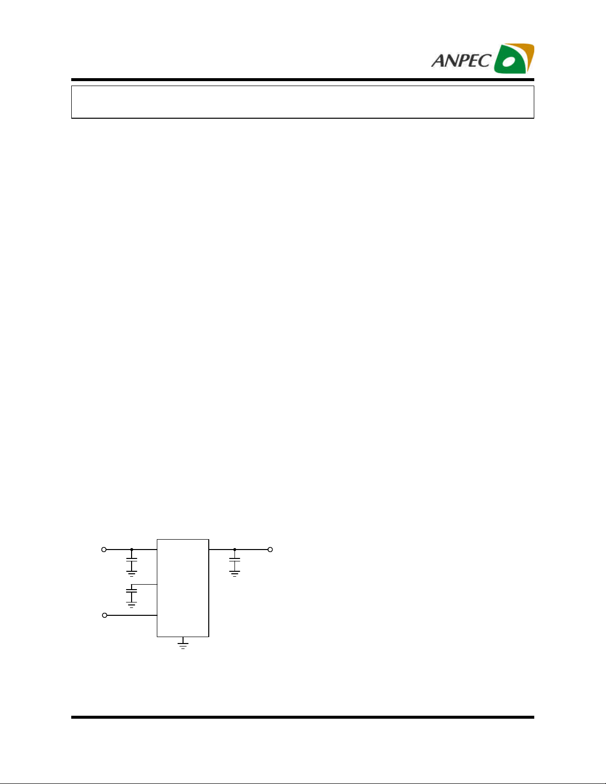
Simplified Application Circuit
APL3512A/B
V
IN
EN
Control
ANPEC reserves the right to make changes to improve reliability or manufacturability without notice, and
advise customers to obtain the latest version of relevant information to verify before placing orders.
Copyright ANPEC Electronics Corp.
Rev. A.6 - Aug., 2012
VIN VOUT
SS
EN/ENB
GND
V
OUT
www.anpec.com.tw1

APL3512
Pin Configuration
VIN 1
SS 2
GND 3
NC 4
SOP-8
APL3512A
VIN 1
SS 2
GND 3
NC 4
SOP-8
APL3512B
8 VOUT
7 NC
6 EN
5 NC
8 VOUT
7 NC
6 ENB
5 NC
VOUT 1
GND 2
EN 3
VOUT 1
GND 2
ENB 3
SOT-23-5
APL3512A
SOT-23-5
APL3512B
Ordering and Marking Information
APL3512
Assembly Material
Handling Code
Temperature Range
Package Code
EN Function
5 VIN
4 SS
5 VIN
4 SS
Package Code
B : SOT-23-5 K : SOP-8 QB : TDFN2x2-6
Operating Ambient Temperature Range
I : -40 to 85 oC
Handling Code
TR : Tape & Reel
EN Function
A : Active High B : Active Low
Assembly Material
G : Halogen and Lead Free Device
VIN 1
SS 2 5 NC
GND 3
TDFN2x2-6
APL3512A
VIN 1
SS 2 5 NC
GND 3
TDFN2x2-6
APL3512B
Exposed Pad, connect to large
ground plane for heat dissipation
6 VOUT
4 EN
6 VOUT
4 ENB
APL3512A B: L2AX X - Date Code
APL3512B B: L2BX X - Date Code
APL3512A K:
APL3512B K: XXXXX - Date Code
APL3512A QB: X - Date Code
APL3512B QB: X - Date Code
Note : ANPEC lead-free products contain molding compounds/die attach materials and 100% matte tin plate termination finish; which
are fully compliant with RoHS. ANPEC lead-free products meet or exceed the lead-free requirements of IPC/JEDEC J-STD-020D for
MSL classification at lead-free peak reflow temperature. ANPEC defines “Green” to mean lead-free (RoHS compliant)and halogen
free (Br or Cl does not exceed 900ppm by weight in homogeneous material and total of Br and Cl does not exceed 1500ppm by
weight).
Copyright ANPEC Electronics Corp.
Rev. A.6 - Aug., 2012
APL3512A
XXXXX
APL3512B
XXXXX
L12A
X
L12B
X
XXXXX - Date Code
www.anpec.com.tw2
APL3512
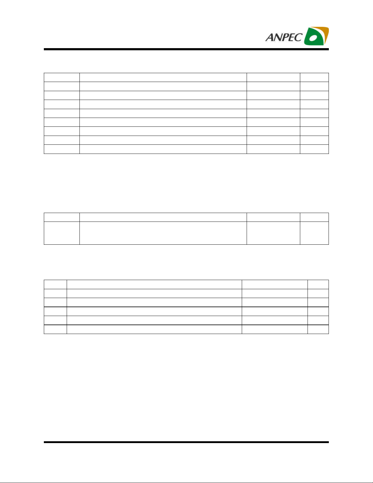
Absolute Maximum Ratings (Note 1)
Symbol Parameter Rating Unit
VIN VIN to GND Voltage -0.3 ~ 6 V
V
VOUT to GND Voltage -0.3 ~ 6 V
OUT
V
, VEN EN, ENB to GND Voltage -0.3 ~ 6 V
ENB
VSS SS to GND Voltage -0.3 ~ 6 V
o
o
o
o
C/W
C
C
C
I
Continuous Output Current Internally Limited A
OUT
TJ Maximum Junction Temperature -40 ~ 150
T
Storage Temperature -65 ~ 150
STG
T
Maximum Lead Soldering Temperature, 10 Seconds 260
SDR
Note1: Stresses beyond those listed under "absolute maximum ratings" may cause permanent damage to the device. These are
stress ratings only and functional operation of the device at these or any other conditions beyond those indicated under "recommended operating conditions" is not implied. Exposure to absolute maximum rating conditions for extended periods may affect device
reliability.
Thermal Characteristics
Symbol Parameter Typical Value Unit
Junction-to-Ambient Resistance in Free Air
θJA
Note 2: θ
is measured with the component mounted on a high effective thermal conductivity test board in free air.
JA
(Note 2)
SOT-23-5
SOP-8
TDFN2x2-6
250
160
225
Recommended Operating Conditions (Note 3)
Symbol
VIN VIN Input Voltage 2.7 ~ 5.5 V
I
OUT Output Current 0 ~2 A
OUT
CSS SS Pin Soft-Start Capacitor
TA Ambient Temperature -40 ~ 85
TJ Junction Temperature -40 ~ 125
Note 3: Refer to the typical application circuit.
Note 4: Attaching a capacitor on SS pin can adjust the V
rate could become internally controlled as if no CSS.
Copyright ANPEC Electronics Corp.
Rev. A.6 - Aug., 2012
Parameter Range Unit
(Note 4)
0.3 ~470 nF
soft-start rate. If the CSS is out of the recommended range, the soft-start
OUT
www.anpec.com.tw3
o
C
o
C

APL3512
or SS
Electrical Characteristics
Unless otherwise specified, these specifications apply over VIN=5V, VEN=5V or V
TA=25oC.
Symbol
Parameter Test Conditions
SUPPLY CURRENT
VIN Supply Current
No load, VEN=0V or V
No load, VEN=5V or V
Leakage Current VOUT=GND, VEN=0V or V
Reverse Leakage Current VIN=GND, V
OUT
=5V - - 1
ENB
=0V - 60 100
ENB
ENB
=5V, VEN=0V or V
POWER SWITCH
I
=1.5A, TA=25oC - 90 110
R
DS(ON)
Power Switch On Resistance
OUT
I
=1.5A, TA=-40~85oC - 90 140
OUT
UNDER-VOLTAGE LOCKOUT
VIN UVLO Threshold Voltage VIN rising, TA=-40~85oC 2.3 - 2.65 V
VIN UVLO Hysteresis - 0.2 - V
CURRENT-LIMIT AND SHORT-CIRCUIT PROTECTIONS
I
Current-Limit Threshold VIN=2.7V to 5.5V, TA=-40~85oC 2.5 3.1 4.22 A
LIM
I
Short-Circuit Output Current VIN=2.7V to 5.5V - 0.8 - A
SHORT
SOFT-START CONTROL PIN
SS Current VIN=5V, TA=-40~85oC 1 2 3
VIN=5V, No load, C
=1µF, CSS=10nF,
OUT
TA=-40~85oC
tSS Soft-Start Time
VIN=3.3V, No load, C
TA=-40~85oC
VIN=3.3V, No load, C
=1µF, CSS=10nF,
OUT
=1µF, No C
OUT
tied to VIN, TA=-40~85oC
EN OR ENB INPUT PIN
VIH Input Logic HIGH VIN=2.7V to 5V 2 - - V
VIL Input Logic LOW VIN=2.7V to 5V - - 0.8 V
Input Current - - 1
VOUT Discharge Resistance VEN=0V or V
=5V - 150 -
ENB
OVER-TEMPERATURE PROTECTION (OTP)
TOTP Over-Temperature Threshold TJ rising - 140 -
Over-Temperature Hysteresis - 20 -
=0V and TA=-40~85oC. Typic al values are at
ENB
APL3512A/B
Min. Typ. Max.
=5V - - 1
=5V - - 1
ENB
- 10 - ms
- 6.6 - ms
SS
1 2 3 ms
Unit
µA
µA
µA
µA
mΩ
mΩ
µA
µA
Ω
°C
°C
Copyright ANPEC Electronics Corp.
Rev. A.6 - Aug., 2012
www.anpec.com.tw4
APL3512
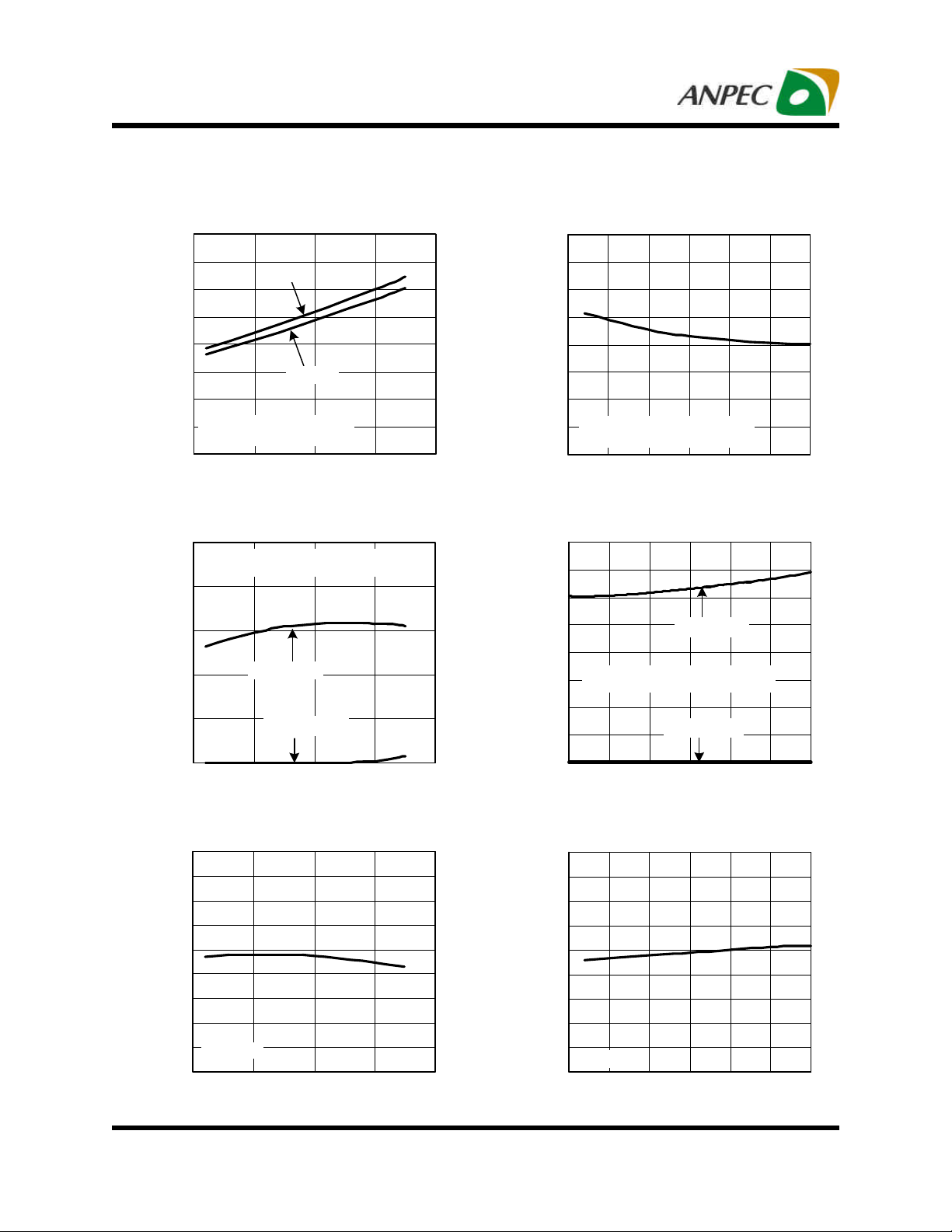
Typical Operating Characteristics
Switch On Resistance vs. Junction
Temperature
160
140
(mΩ)
120
DS(on)
VIN=3.3V
100
80
60
40
I
20
Switch On Resistance , R
=1.5A, C
OUT
C
=10µF/X7R
OUT
0
=1µF/X7R,
IN
-50 0 50 100
Junction Temperature (oC)
Supply Current vs. Junction
Temperature
100
V
=5V, R
IN
C
IN =COUT
80
(µA)
CC
60
40
Supply Current, I
20
LOAD
=33µF/Electrolytic
IC Enabled
IC Disabled
VIN=5V
= Open,
150
Switch On Resistance vs. Input
Voltage
130
120
(mΩ)
110
DS(on)
100
90
80
70
I
60
Switch On Resistance, R
50
=1.5A, C
OUT
C
=1µF/X7R, TA=25oC
OUT
2.5 3.0 3.5 4.0 4.5 5.0 5.5
=1µF/X7R,
IN
Input Voltage (V)
Supply Current vs. Input Voltage
80
70
60
(µA)
CC
50
40
R
= Open,
30
20
Supply Current, I
LOAD
C
IN =COUT
10
IC Enabled
=1µF/X7R, TA=25oC
IC Disabled
0
-50 0 50 100
Junction Temperature (oC)
Current-Limit Threshold vs.
Junction Temperature
3.8
3.6
(A)
3.4
LIM
3.2
3.0
2.8
2.6
2.4
Current-Limit Threshold, I
2.2
V
=5V
IN
2.0
-50 0 50 100
Junction Temperature (oC)
Copyright ANPEC Electronics Corp.
Rev. A.6 - Aug., 2012
150
150
00
2.5 3.0 3.5 4.0 4.5 5.0 5.5
Input Voltage (V)
Current-Limit Threshold vs.
Input Voltage
3.8
3.6
(A)
3.4
LIM
3.2
3.0
2.8
2.6
2.4
Current-Limit Threshold, I
2.2
TA =25oC
2.0
2.5 3.0 3.5 4.0 4.5 5.0 5.5
Input Voltage (V)
www.anpec.com.tw5
APL3512
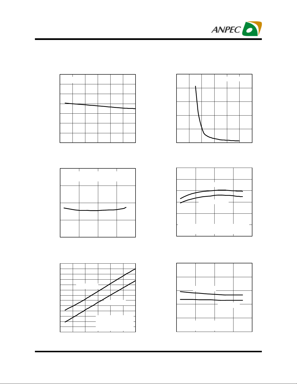
Typical Operating Characteristics (Cont.)
Short-Circuit Output Current vs.
1.4
(A)
SHORT
TA=25oC
1.2
1.0
0.8
0.6
0.4
0.2
Short-Circuit Output Current, I
0.0
2.5 3.0 3.5 4.0 4.5 5.0 5.5
Input Voltage
Input Voltage (V)
Turn-On Rising Time vs. Junction
Temperature
2.0
V
= 5V, R
IN
C
= 1µF/X7R, C
IN
(ms)
1.5
F
1.0
LOAD
=30Ω,
=33µF/Electrolytic
OUT
Current-Limit Response vs.
Output Peak Current
250
200
150
100
50
Current-Limit Response (µs)
0
0 2 4 6 8 10 12
Output Peak Current (A)
V
IN
VIN UVLO Threshold Voltage vs.
Junction Temperature
3.2
(V)
2.8
VLOC
2.4
2.0
UVLO Rising
UVLO Falling
=5V, TA=25oC
0.5
Turn-On Rising Time, t
0.0
-50 0 50 100
Junction Temperature (oC)
EN Pin Threshold Voltage vs.
2.1
2.0
(V)
1.9
EN
1.8
1.7
1.6
1.5
1.4
1.3
1.2
1.1
1.0
EN Pin Threshold Voltage, V
0.9
0.8
2.5 3.0 3.5 4.0 4.5 5.0 5.5
Input Voltage
EN Rising
R
C
Elctrolytic, TA=25oC
Input Voltage (V)
EN Falling
=50Ω,
LOAD
= C
IN
OUT
=33µF/
150
1.6
1.2
I
=15mA,
UVLO Threshold Voltage, V
IN
V
OUT
C
= 1µF/X7R, C
0.8
IN
-50 0 50 100
OUT
Junction Temperature (oC)
EN Pin Threshold Voltage vs.
Junction Temperature
3.0
(V)
2.5
EN
2.0
1.5
1.0
EN Pin Threshold Voltage, V
V
C
0.5
-50 0 50 100
EN Rising
=5V, R
IN
= C
IN
=50Ω,
LOAD
=33µF/Elctrolytic
OUT
Junction Temperature (oC)
=33µF/Electrolytic
150
EN Falling
150
Copyright ANPEC Electronics Corp.
Rev. A.6 - Aug., 2012
www.anpec.com.tw6
APL3512
Typical Operating Characteristics (Cont.)
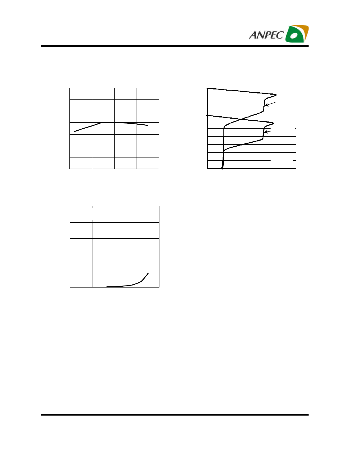
SS Current vs. Junction Temperature
3.2
2.8
2.4
(µA)
SS
2.0
1.6
1.2
SS Current, I
0.8
V
=5V
IN
0.4
-50 0 50 100
Junction Temperature (oC)
Turn Off Leakage Current vs.
Junction Temperature
10
V
= 5V, R
IN
C
(µA)
8
LEAK
= C
IN
OUT
6
= 0Ω,
LOAD
=1µF/X7R
150
Output Voltage vs. Output Current
5.0
4.5
4.0
(V)
3.5
OUT
3.0
2.5
2.0
1.5
Output Voltage, V
1.0
0.5
0.0
0 1 2 3 4
Output Current (A)
VIN=5V
VIN=3.3V
TA=25oC
4
2
Turn Off Leakage Current, I
0
-50 0 50 100
Junction Temperature (oC)
150
Copyright ANPEC Electronics Corp.
Rev. A.6 - Aug., 2012
www.anpec.com.tw7
 Loading...