

ANPEC APL1565A-33KC-TU, APL1565A-33KC-TR, APL1565A-28KC-TU, APL1565A-28KC-TR, APL1565A-25KC-TU Datasheet
...
Copyright ANPEC Electronics Corp.
Rev. A.3 - Oct., 2002
APL1565A
www.anpec.com.tw1
ANPEC reserves the right to make changes to improve reliability or manufacturability without notice, and advise
customers to obtain the latest version of relevant information to verify before placing orders.
1A Low Dropout, Fast Response Fixed Voltage Regulator
••
••
•
Guaranteed Output Voltage Accuracy within 2%
••
••
•
Fast Transient Response
••
••
•
Load Regulation : 1mV Typ.
••
••
•
Line Regulation : 4mV Typ.
••
••
•
Low Dropout Voltage : 210mV at I
OUT
=1A
••
••
•
Current Limit : 1A Typ. at TJ=125 °C
••
••
• On-Chip Thermal Limiting : 150 °C Typ.
••
••
• Standard 8-pin SO Power Package
••
••
• Very Low Shutdown Current : < 0.5µA
••
••
• Fixed Output Voltage : 2.5V, 2.8V and 3.3V
Features
Applications
••
••
• Peripheral Cards
••
••
• Active SCSI Terminators
••
••
• Low Voltage Logic Supplies
••
••
• Post Regulator for Switching Power Supply
General Description
The APL1565A is a low dropout regulators operate
from 2.7V to 6V input voltage and deliver up to 1A
current capability. In order to obtain lower dropout
voltage and faster transient response, which is critical for low voltage applications, the APL1565/A has
been optimized.
The device is available in fixed output voltages of
2.5V,2.8V and 3.3V. APL1565A Dropout voltage is
guaranteed at a maximum of 210mV at 1A load.
Current limit is trimmed to ensure specified output
current and controlled short-circuit current. On-chip
thermal limiting provides protection against any combination of overload that would create excessive junction temperatures.
The APL1565A is available in the industry standard
8-pin SO power package which can be used in applications where space is limited.
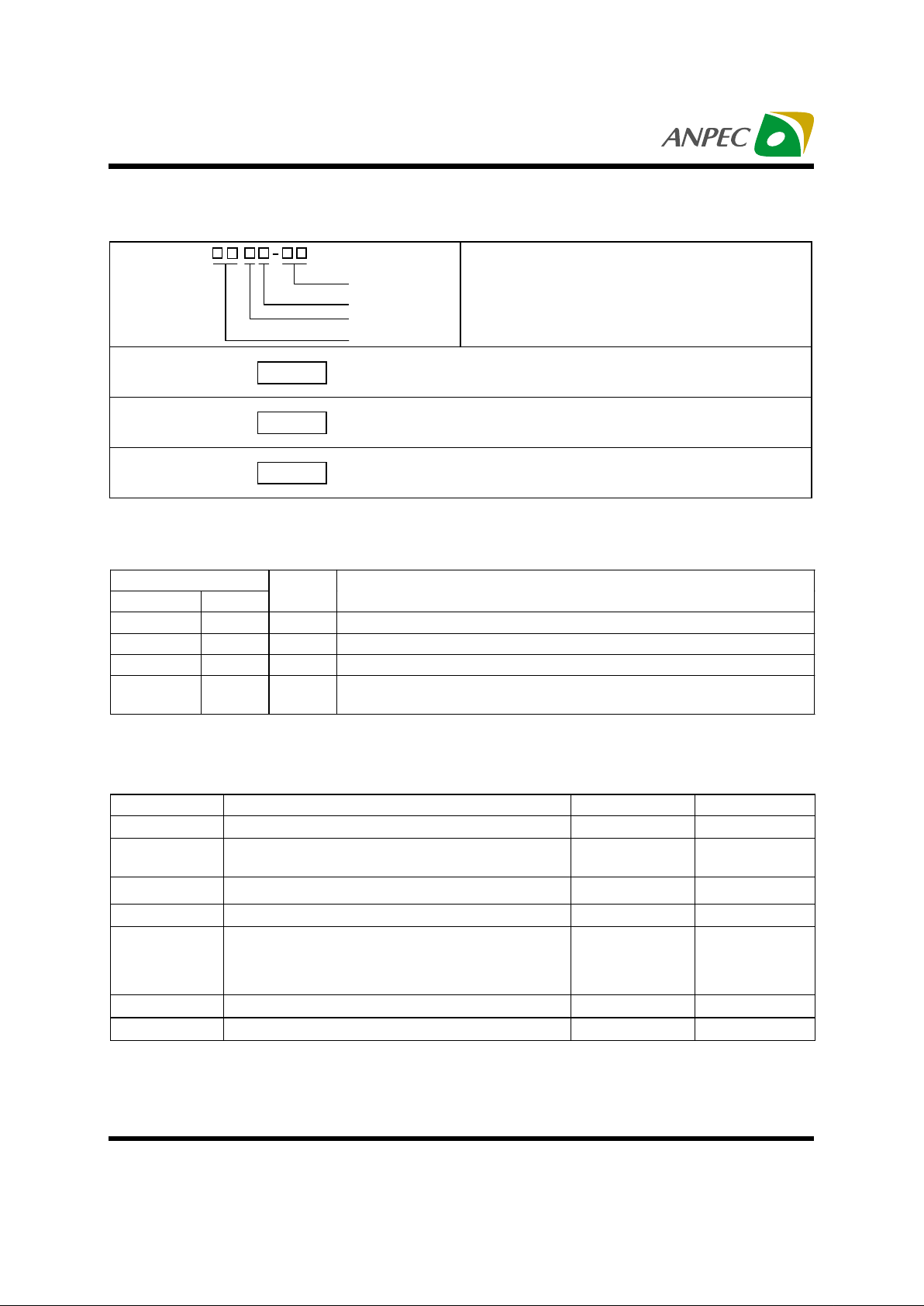
Pin Configuration
1
2
3
45
6
7
8EN
V
IN
V
OUT
NC GND
GND
GND
GND
APL1565A
Front View for SO - 8
Copyright ANPEC Electronics Corp.
Rev. A.3 - Oct., 2002
APL1565A
www.anpec.com.tw2
PIN
No. Name
I/O Description
(1)
Note1
EN I Enable control pin, low = off , high = normal .
2VINI Supply voltage input.
3V
OUT
O Output pin of the regulator.
5(6,7,8)
Note1
GND
Ground pins of the circuitry, and all ground pins must be soldered to
PCB with proper power dissipation.
Symbol Parameter Rating Unit
VIN, V
OUT
Input Voltage or Out Voltage 6 V
EN Enable Control Pin 6 V
R
TH,JA
Thermal Resistance – Junction to Ambient 210
°
C/W
P
D
Power Dissipation Internally Limited W
T
J
Operating Junction Temperature
°
C
Control Section 0 to 125
Power Transistor 0 to 150
T
STG
Storage Temperature Range -65 to +150
°
C
T
L
Lead Temperature (Soldering, 10 second) 260
°
C
Package C ode
K : SOP-8
Tem p. Range
C : 0 to 70 C
Handling Code
TU : Tube TR : Tape & Reel
Voltage Code
25 : 2.5V 28 : 2.8V 33: 3.3V
°
APL15 65A -
Handling Code
Tem p. Range
Package C ode
Voltage Code
APL1565A -25K :
APL1565A
XXXXX25
XXXXX - Date Code
APL1565A -28K :
APL1565A
XXXXX28
XXXXX - Date Code
APL1565A -33K :
APL1565A
XXXXX33
XXXXX - Date Code
Ordering and Marking Information
Absolute Maximum Ratings
Pin Description
Copyright ANPEC Electronics Corp.
Rev. A.3 - Oct., 2002
APL1565A
www.anpec.com.tw3
APL1565A
Symbol Parameter Test Conditions
Min. Typ. Max.
Unit
V
IN
Input Voltage 2.7 6 V
V
OUT
Output Voltage V
OUT
+1.0V< VCC<6.0V, 0mA< I
OUT
< I
MAX
V
OUT
-2
%
V
OUT
V
OUT
+2
%
V
I
LIMIT
Circuit Current Limit
1.0 1.2 A
REG
LINE
Line Regulation V
OUT
+0.5V< VCC<6.0V, 0mA< I
OUT
< I
MAX
410mV
REG
LOAD
Load Regulation VIN =V
OUT
+1.0V, 0mA< I
OUT
< I
MAX
1
6
mV
V
DROP
Dropout Voltage
I
OUT
=1A, Tj = 0~125°C
210 400 mV
PSRR Ripple Rejection
F≤1kHz, 1Vpp at V
IN
= V
OUT
+1.0V
55 65 dB
No load 50 100
I
Q
Quiescent Current
I
OUT
=1A 370 300
µ
A
Shutdown Supply
Current
EN = low
I
OUT
=0, VCC =6.0V
0.01 1
µ
A
V
IH
1.8
V
IL
Enable Pin
Threshold
V
IN
=3.3V
0.4
V
150
°
C
OTS Over Temperature
Hysteries 10
°
C
TC
Output Voltage
Temperature
Coefficient
50 ppm/°C
Electrical Characteristics
Unless otherwise noted these specifications apply over full temperature , VIN=3.6V, CIN=COUT=4.7uF, EN=VIN,
TJ=0 to 125°C . Typical values refer to TJ=25°C .
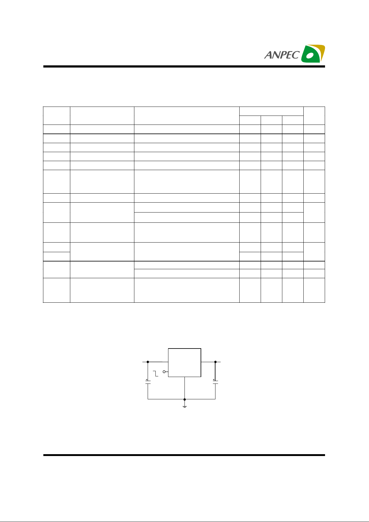
Application Circuit
APL1565A
IN
OUT
GND
V
IN
=5V
C
OUT
10uF
V
OUT
=3.3V
C
IN
10F
EN
ON
OFF
5V to 3.3V Regulation with Enable Function

Copyright ANPEC Electronics Corp.
Rev. A.3 - Oct., 2002
APL1565A
www.anpec.com.tw4
Reverse Current Protection
The APL1565A have an internal reverse protection,
it does not need an external schottky diode to connect the regulator input and output. If the output voltage is forced above the input voltage by more than
11mV, the IC will be shutdown and the ground pin
current is below 0.1uA.
Application Information
Capacitor Selection and Regulator
Stability
The APL1565A use at least a 4.7µF capacitor on the
input. This capacitor can use Aluminum, Tantalum or
Ceramic capacitors. Input capacitor with large values and low ESR provide better PSRR and line-transient response. The output capacitor also can use
Aluminum, Tantalum or Ceramic capacitors, and a
minimum value of 10µF and ESR above 0.06Ω is
recommended. A larger output capacitor can reduce
noise and improve load-transient response, stability
and PSRR.
The APL1565A load-transient response graphs in
typical characteristics show the transient response.
A step change in the load current from 0mA to 1A at
1us will cause a 100mV transient spike. Larger output capacitor and lower ESR can reduce transient
spike.
Load-Transient Considerations
The minimum input-output voltage difference
(dropout) determines the lowest usable supply
voltage. In battery-powered systems, this will determine the useful end-of-life battery voltage. Because
the APL1565A use a p-channel MOSFET pass
transistor, the dropout voltage is a function of drainto-source on-resistance (R
DS(ON)
) multiplied by the load
current.
Input-Output (Dropout)Voltage
Current Limit
The APL1565A have a current limit protection. The
ouptut voltage will drop close to zero volt, when load
current reaches the limit, and then the load current
will be limited at 150mA after output voltage is below
0.7V. When the load current back to the value where
limiting started, the output voltage and current will
return to normal value. When output is shorted to
ground, the APL1565/A will keep short circuit current
at 150mA .
Thermal protection limits total power dissipation in
the device. When the junction temperature exceeds
TJ=+150J, the thermal sensor generates a logic signal to turn off the pass transistor and allows IC to
cool. When the IC’s junction temperature is down by
10J, the thermal sensor will turn the pass transistor
on again, resulting in a pulsed output during continuous thermal protection. Thermal protection is designed to protect it in the event of fault conditions.
For continuous operation, do not exceed the absolute maximum junction temperature of TJ=+150J.
Thermal Protection

Copyright ANPEC Electronics Corp.
Rev. A.3 - Oct., 2002
APL1565A
www.anpec.com.tw5
Application Information (Cont.)
Operating Region and Power Dissipation
The thermal resistance of the case to circuit board,
and the rate of air flow all control the APL1565A’s
maximum power dissipation. The power dissipation
across the device is PD = I
OUT (VIN-VOUT
) and the maximum power dissipation is:
P
DMAX
= (TJ-TA) / (?JC + ?CA)
where T
J-TA
is the temperature difference between
the junction and ambient air, ?JC is the thermal resistance of the package, and?CA is the thermal resistance through the printed circuit board, copper
traces, and other materials to the ambient air.
The GND pin of the APL1565A provide an electrical
connection to ground and channeling heat away. If
power dissipation is large, connect the GND pin to
ground using a large pad or ground plane, can improve the problem of over heat of IC.

Copyright ANPEC Electronics Corp.
Rev. A.3 - Oct., 2002
APL1565A
www.anpec.com.tw6
Package Information
Millimeters Inches
Dim
Min. Max. Min. Max.
A 1.35 1.75 0.053 0.069
A1 0.10 0.25 0. 004 0.010
D 4.80 5.00 0.189 0.197
E 3.80 4.00 0.150 0.157
H 5.80 6.20 0.228 0.244
L 0.40 1.27 0.016 0.050
e1 0.33 0.51 0.013 0.020
e2 1.27BSC 0.50BSC
φ
18
°
8
°
HE
e1 e2
0.015X45
D
A
A1
0.004max.
1
L
SOP-8 pin ( Reference JEDEC Registration MS-012)

Copyright ANPEC Electronics Corp.
Rev. A.3 - Oct., 2002
APL1565A
www.anpec.com.tw7
Physical Specifications
Pre-heat temperature
183 C
Peak temperature
Time
°
temperature
Classification Reflow Profiles
Convection or IR/
Convection
VPR
Average ramp-up rate(183°C to Peak) 3°C/second max. 10 °C /second max.
Preheat temperature 125 ± 25°C)
120 seconds max
Temperature maintained abov e 183°C
60 – 150 seconds
Time within 5°C of actual peak temperature
10 –20 seconds 60 seconds
Peak temperature range
220 +5/-0°C or 235 +5/-0°C 215-219°C or 235 +5/-0°C
Ramp-down rate
6 °C /second max. 10 °C /second max.
Time 25°C to peak temperature
6 minutes max.
Package Reflow Conditions
pkg. thickness
≥≥≥≥
2.5mm
and all bgas
pkg. thickness < 2.5mm and
pkg. volume
≥≥≥≥
350 mm³
pkg. thickness < 2.5mm and pkg.
volume < 350mm³
Convection 220 +5/-0 °C Convection 235 +5/- 0 °C
VPR 215-219 °C VPR 235 +5/-0 °C
IR/Convection 220 +5/-0 °C IR/Convection 235 +5/-0 °C
Terminal Material Solder-Plated Copper (Solder Material : 90/10 or 63/37 SnPb)
Lead Solderability Meets EIA Specification RSI86- 91, A NSI/J-STD-002 C a teg ory 3 .
Reference JEDEC Standard J-STD-020A APRIL 1999
Reflow Condition (IR/Convection or VPR Reflow)

Copyright ANPEC Electronics Corp.
Rev. A.3 - Oct., 2002
APL1565A
www.anpec.com.tw8
Rel iability te s t p ro g r am
Test item Method Description
SOLDERABILITY M IL-STD-883D-2003
245°C , 5 SEC
HOLT MIL-STD-883D-1005.7
1000 Hrs Bias @ 125 °C
PCT JESD-22-B, A102
168 Hrs, 100 % RH , 121°C
TST MIL-STD-883D-1011.9
-65°C ~ 150°C, 200 C y c les
ESD MIL-STD-883D-3015.7 VHBM > 2KV, VMM > 200V
Latch-U p JESD 78 10ms , Itr > 100mA
Carrier Tape
A
J
B
T2
T1
C
t
Ao
E
W
Po
P
Ko
Bo
D1
D
F
P1
Application A B C J T1 T2 W P E
330 ± 162 +1.5
12.75+
0.15
2 ± 0.5 12.4 ± 0.2 2 ± 0.2 12± 0. 3 8± 0.1 1.75±0.1
F D D1 Po P1 Ao Bo Ko tSOP- 8
5.5± 1 1.55 +0.1 1.55+ 0.25 4.0 ± 0.1 2.0 ± 0.1 6.4 ± 0.1 5.2± 0. 1 2.1± 0.1 0 .3±0.013

Copyright ANPEC Electronics Corp.
Rev. A.3 - Oct., 2002
APL1565A
www.anpec.com.tw9
Customer Service
Anpec Electronics Corp.
Head Office :
5F, No. 2 Li-Hsin Road, SBIP,
Hsin-Chu, Taiwan, R.O.C.
Tel : 886-3-5642000
Fax : 886-3-5642050
Taipei Branch :
7F, No. 137, Lane 235, Pac Chiao Rd.,
Hsin Tien City, Taipei Hsien, Taiwan, R. O. C.
Tel : 886-2-89191368
Fax : 886-2-89191369
Cover Tape Dimensions
Application Carrier Width Cover Tape Width Devices Per Reel
SOP- 8
12 9.3 2500
 Loading...