

查询APU0594WE-TY供应商
APL1085
3A Low Dropout Fast Response Positive Adjustable Regulator and Fixed 3.3V
Features General Description
••
• Fast Transient Response
••
••
• Guaranteed Dropout Voltage at Multiple Cur-
••
rents
••
• Load Regulation : 0.05% Typ.
••
••
• Line Regulation : 0.03% Typ.
••
••
• Low Dropout Voltage : 1.2V Typ. at I
••
••
• Trimmed Current Limit : 3A Typ. at T
••
••
• On-Chip Thermal Limiting : 150 °C Typ.
••
••
• Standard 3-pin TO-220 , TO-252 and TO-263
••
=3A
OUT
=125 °C
J
Power Package
Applications
••
• Pentium
••
••
• PowerPC
••
••
• Low Voltage Logic Supplies
••
••
• Battery-Powered Circuitry
••
••
• Post Regulator for Switching Power Supply
••
TM
Processor Supplies
TM
Supplies
The APL1085 is a low dropout three-terminal adjustable regulator with 3A output current capability. In
order to obtain lower dropout voltage and faster transient response, which is critical for low voltage
applications, the APL1085 has been optimized. The
output available voltage range of adjustable version
is from 1.25~5.75V with an input supply below 7V ,
and the fixed 3.3V output voltage device is also
available.
Current limit is trimmed to ensure specified output
current and controlled short-circuit current. On-chip
thermal limiting provides protection against any combination of overload that would create excessive junction temperatures.
The APL1085 is available in both the through-hole
and surface mount versions of the industry standard
Pin Description
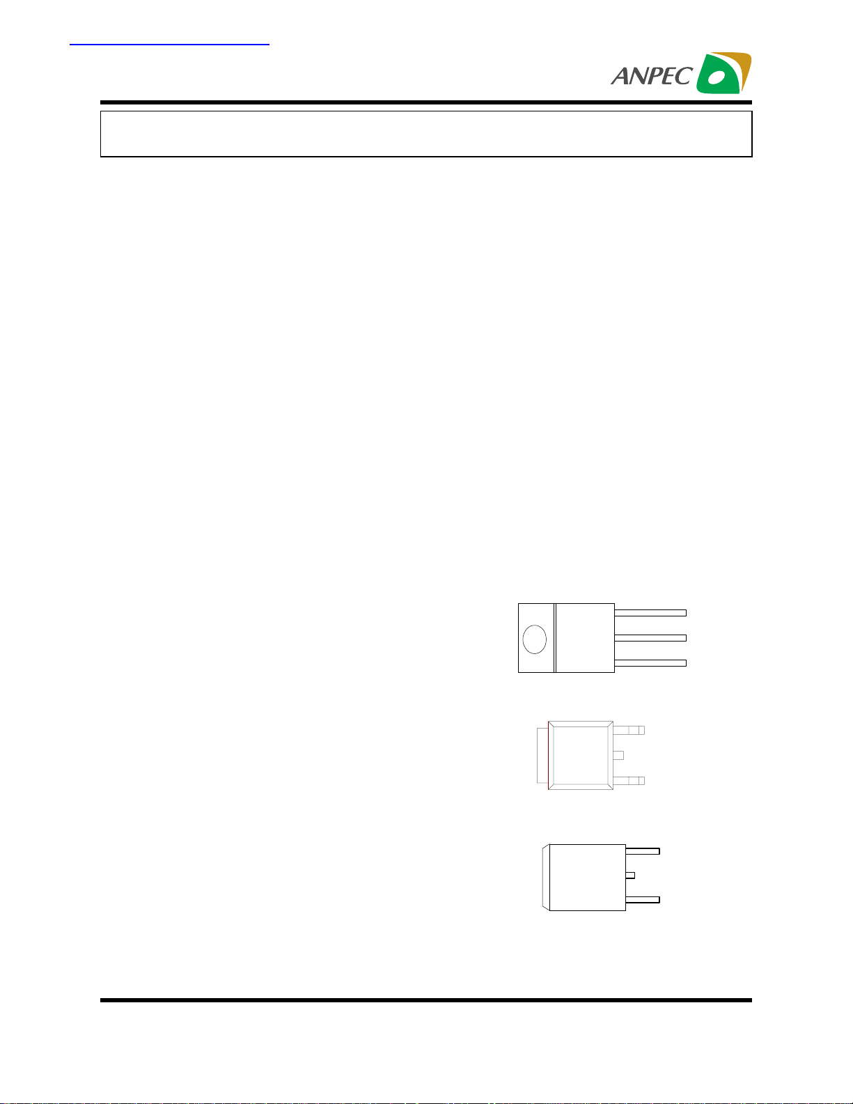
TAB is V
OUT
3
2
1
V
IN
V
OUT
ADJ
Front View APL1085 TO-220 Package
V
IN
V
OUT
ADJ
TAB is V
OUT
3
2
1
Front View APL1085 TO-252 Package
V
IN
V
OUT
ADJ
TAB is V
OUT
3
2
1
Front View APL1085 TO-263 Package
ANPEC reserves the right to make changes to improve reliability or manufacturability without notice, and advise
customers to obtain the latest version of relevant information to verify before placing orders.
Copyright ANPEC Electronics Corp.
Rev. B.5 - Jun., 2003
www.anpec.com.tw1
APL1085
Ordering Information
APL1085 -
AP L1085:
AP L1085
XXXXX
Lead Free Code
Handling Code
Tem p. Range
Package C ode
Voltage Code
XXXXX
- D a te C od e
Package C ode
F : TO-220 G : TO-263
U : TO-252
Tem p. Range
C : 0 to 70 C
Handling Code
TU : Tube TR : Tape & Reel
Voltage Code :
33 : 3.3V Blank : Adjustable Version
Lead Free Code
L : Lead Free Device Blank : Original Device
AP L1085-33 :
°
33
AP L1085
XXXXX
XXXXX
- D a te C od e
Absolute Maximum Ratings
Symbol Parameter Rating Unit
V
T
T
STG
T
Input Voltage 7 V
I
Operating Junction Temperature Range
J
Control Section
Power Transistor
0 to 125
0 to 150
Storage Temperature Range -65 to +150
Lead Temperature (Soldering, 10 second) 260
L
C
°
C
°
C
°
Electrical Characteristics
V
V
REG
REG
I
LIMIT
I
Reference Voltage
REF
Output Voltage
OUT
Line Regulation
LINE
Load Regulation
LOAD
V
Dropout Voltage
D
Current Limit
Adjust Pin Current
ADJ
APL1085-3.3
APL1085
APL1085-3.3
APL1085
APL1085-3.3
1.5V≤(V
10mA≤ I
10mA≤ I
T
J
T
J
2.75V≤V
4.75V≤V
T
J
(V
V
I N
V
∆
(V
IN -VOUT
OUT
OUT
=0~125°C
=0~125°C, (Notes 1)
≤
IN
≤
IN
=25°C, (Notes 1)
=3V, 10mA≤ I
)
IN -VOUT
=5V, 0mA≤ I
=1% ,I
REF
=1.7V, T
)
IN -VOUT
T
(V
IN -VOUT
=3V, T
)
T
(V
T
=0∼
J
IN -VOUT
=3V, I
)
125°C
≤5.75V,
)
=0~125°C
3A, T
≤
≤
J
3A, 4.75V≤V
7V, I
7V, I
OUT
=
OUT
=
OUT
≤
OUT
=3A ,T
=10mA,
OUT
10mA,
0mA ,
3A
J
7V,
≤
IN
3A
≤
OUT
=0~125°C
C
=25°
J
125°C
=
J
C
=25°
J
125°C
=
J
APL1085Symbol Parameter Test Conditions
Unit
Min. Typ. Max.
1.225(-2%) 1.250 1.275(+2%) V
3.235(-2%) 3.300 3.365(+2%) V
0.03 0.2 %
%
0.05
0.05
0.3
0.5
1.3 1.4 V
4.5
3.5
5.0
4.0
6.0
5.0
6.5
5.5
60 120
µ
A
A
Copyright ANPEC Electronics Corp.
Rev. B.5 - Jun, 2003
www.anpec.com.tw2
APL1085
Electrical Characteristics Cont.
APL1085Symbol Parameter Test Conditions
Unit
Min. Typ. Max.
∆
I
Adjust Pin Current
I
ADJ
Change APL1085
Minimum Load
LMIN
Current APL1085
I
Quiescent Current
Q
≤
3A
)≤5.75V,
)≤5.75V,
1.5V≤( V
10mA≤ I
1.5V≤( V
T
=0∼
J
V
I N
IN -VOUT
OUT
IN -VOUT
125°C
=5V 8 13 mA
0.2 5
210mA
APL1085-3.3
PSRR Ripple Rejection
L
Long -Term
S
F=120Hz, C
(V
IN -VOUT
T
=
J
)=3V, I
125°C,1000Hrs.
=22µF, Ta nt . ,
out
=3A
OUT
60 dB
0.03 1.0 %
Stability
V
N
θ
JC
RMS Output
Noise(% of V
Thermal
Resistance
OUT
T
C,10Hz? F? 10kHz
=25°
J
)
Control Circuitry/Power
Transistor
0.003 %
0.7/3.0
°
Junction to Case
NOTE 1: See thermal regulation specifications for changes in output voltage due to heating effects. Load and line regulations are
measured at a constant junction temperature by low duty cycle pulse testing.
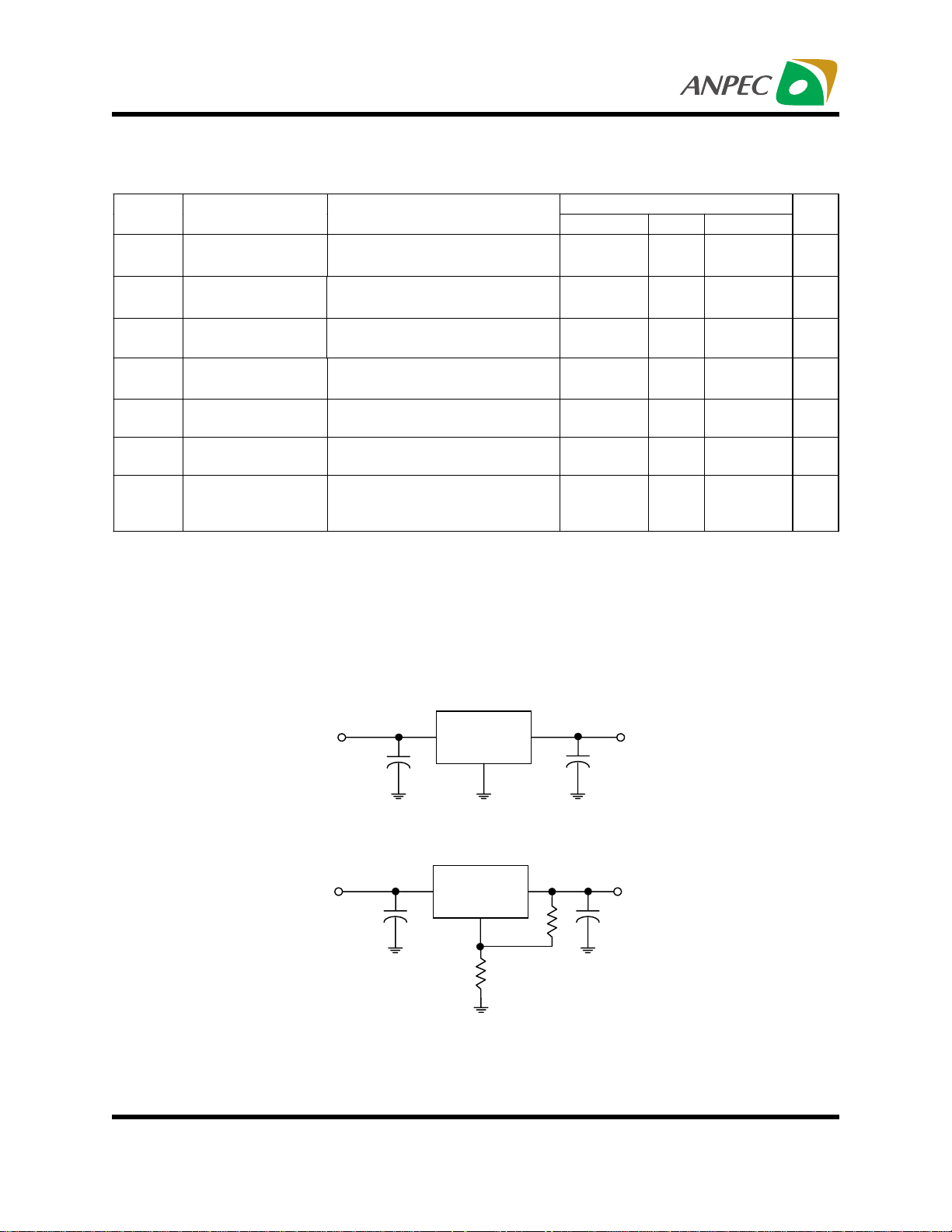
Application Circuits
A
µ
C/
W
(2.75V~7V)
V
IN
V
(5V)
IN
10µ
10µ
C
*Required for stability
APL1085:C2=10µF
* R1 is typically in range of 100Ω to 120Ω
Copyright ANPEC Electronics Corp.
Rev. B.5 - Jun, 2003
Typical Regulator
+
F
C
1
APL1085
+
Solid Tantalum
C
2*
(1.250V/ 3A)
V
OUT
5V to 3.3V Regulator
+
F
1
APL1085
+
R1
R2
R1/(R1+R2)=1.250V/3.3V
V
(3.3V/ 3A)
OUT
Solid Tantalum
C
2*
www.anpec.com.tw3
APL1085
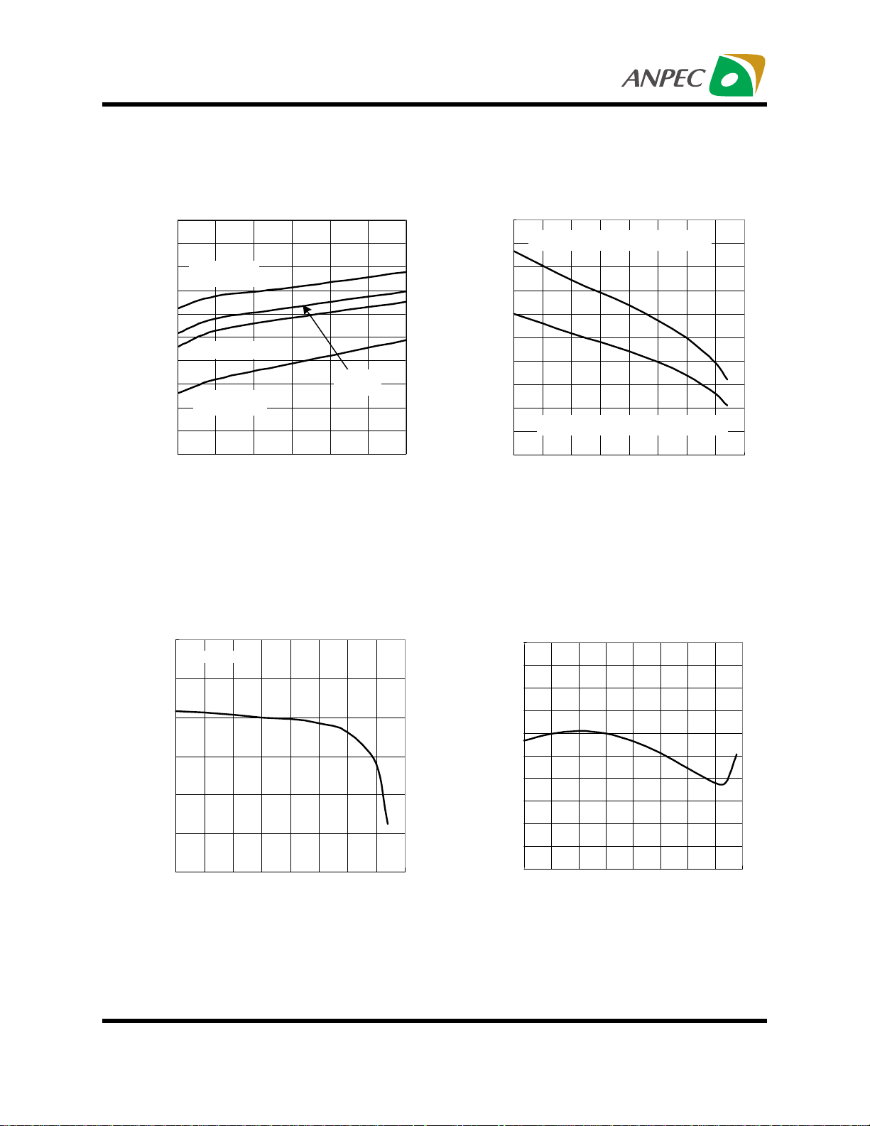
Typical Characteristics
Dropout Voltage vs Output Current
1.5
1.4
1.3
TJ= -50°C
1.2
1.1
1.0
0.9
0.8
Dropout Voltage (V)
0.7
TJ= 25°C
TJ=125°C
0.6
0.5
0 0.5 1 1.5 2 2.5 3
Output Current (A)
TJ=0°C
Short-Circuit Current vs Temperature
14
13
VIN-V
OUT (SHORT CIRCUIT)
=5V
12
11
10
9
8
7
Shout- Circuit Current (A)
6
5
4
-50 0 50 100 150
VIN-V
OUT(SHORT CIRCUIT)
=3.3V
Temperature (°C)
Load Regulation vs Temperature
0.10
∆
I =3A
0.05
0.0
-0.05
-0.10
-0.15
Output Voltage Deviation (%)
-0.20
-50 0 50 100 150
Temperature (°C)
Reference Voltage vs Temperature
1.275
1.270
1.265
1.260
1.255
1.250
1.245
1.240
1.235
Reference Voltage (V)
1.230
1.225
-50 0 50 100 150
Temperature (°C)
Copyright ANPEC Electronics Corp.
Rev. B.5 - Jun, 2003
www.anpec.com.tw4

APL1085
Typical Characteristics (Cont.)
Minimum Load Current vs Temperature
5
4
3
2
1
Minimum Load Current (mA)
0
-50 0 50 100 150
Temperature (°C)
Adjust Pin Current vs Temperature
100
90
80
70
60
50
40
30
Adjust Pin Current (µA)
20
10
0
-50 0 50 100 150
Temperature (°C)
Ripple Rejection vs Frequency
90
80
70
60
50
40
30
VIN-V
20
Ripple Rejection (dB)
10
V
RIPPLE(p-p)
I
OUT
OUT
= 3A
= 3V
= 1V
0
10 100 1k 10k 100k
Frequency (Hz)
Maximum Power Dissipation*
20
18
16
14
12
10
8
6
Power (W)
4
2
0
50 70 90
110 130 150
Case Temperature (°C)
* as Limited by Maximum Jcnction Temperature
Copyright ANPEC Electronics Corp.
Rev. B.5 - Jun, 2003
www.anpec.com.tw5

APL1085
Package Information
TO-220 ( Reference JEDEC Registration TO-220)
D
Q
R
E
L1
b
e
b1
e1
H1
A
F
L
c
J1
Millimeters Inches
Dim
Min. Max. Min. Max.
A 3.56 4.83 0.140 0.190
b1 1.14 1.78 0.045 0.070
b 0.51 1.14 0.020 0.045
c 0.31 1.14 0.012 0.045
D 14.23 16.51 0.560 0.650
e 2.29 2.79 0.090 0.110
e1 4.83 5.33 0.190 0.210
E 9.65 10.67 0.380 0.420
F 0.51 1.40 0.020 0.055
H1 5.84 6.86 0.230 0.270
J1 2.03 2.92 0.080 0.115
L 12.7 14.73 0.500 0.580
L1 3.65 6.35 0.143 0.250
R 3.53 4.09 0.139 0.161
Q 2.54 3.43 0.100 0.135
Copyright ANPEC Electronics Corp.
Rev. B.5 - Jun, 2003
www.anpec.com.tw6

APL1085
Package Information
TO-252( Reference JEDEC Registration TO-252)
E
b2
L2
L1
A
C1
D
H
L
Dim
b
e1
D1
E1
Millimeters Inches
Min. Max. Min. Max.
C
A1
A 2.18 2.39 0.086 0.094
A1 0.89 1.27 0.035 0.050
b 0.508 0.89 0.020 0.035
b2 5.207 5.461 0.205 0.215
C 0.46 0.58 0.018 0.023
C1 0.46 0.58 0.018 0.023
D 5.334 6.22 0.210 0.245
D1 5.2 REF 0.205 REF
E 6.35 6.73 0.250 0.265
E1 5.3 REF 0.209 REF
e1 3.96 5.18 0.156 0.204
H 9.398 10.41 0.370 0.410
L 0.51 0.020
L1 0.64 1.02 0.025 0.040
L2 0.89 2.032 0.035 0.080
Copyright ANPEC Electronics Corp.
Rev. B.5 - Jun, 2003
www.anpec.com.tw7

APL1085
b
0.020.039
c
0.045
0.055
0.090
0
0
Package Information
TO-263
E
L2
A
c2
D
L
L1
L3
e
b2
b
c
Dim
A 4.06 4.83 0.160 0.190
b2 1.14 1.399 0.045 0.055
c 0.38 TYP. 0.015 TYP.
2
D 8.64 9.65 0.340 0.380
E 9.66 10.299 0.380 0.405
e
L 14.60 15.88 0.575 0.625
L1 2.24 2.84
L2
L3 1.20 1.78 0.050 0.070
Copyright ANPEC Electronics Corp.
Rev. B.5 - Jun, 2003
Min. Max. Min. Max.
0.51 0.992
1.14 1.40
Millimeters Inches
2.543 BSC. 0.100 BSC.
-2.92
-0.115
.11
www.anpec.com.tw8

APL1085
Physical Specifications
Terminal Material Solder-Plated Copper (Solder Material : 90/10 or 63/37 SnPb), 100%Sn
Lead Solderability Meets EIA Specification RSI86-91, ANSI/J-STD-002 Category 3.
Reflow Condition (IR/Convection or VPR Reflow)
T
P
Ramp-up
T
L
Tsmax
Tsmin
Temperature
ts
Preheat
25
°
t 25 C to Peak
Classificatin Reflow Profiles
tp
Ramp-down
Time
Critical Zone
T
to T
L
P
t
L
Profile Feature Sn-Pb Eutectic Assembly Pb-Free Assembly
Average ramp-up rate
(T
to TP)
L
Preheat
- Temperature Min (Tsmin)
- Temperature Max (Tsmax)
- Time (min to max) (ts)
Time maintained above:
- Temperature (T
- Time (t
)
L
)
L
3°C/second max. 3°C/second max.
100°C
150°C
60-120 seconds
183°C
60-150 seconds
150°C
200°C
60-180 seconds
217°C
60-150 seconds
Peak/Classificatioon Temperature (Tp) See table 1 See table 2
Time within 5°C of actual
Peak Temperature (tp)
Ramp-down Rate
Time 25°C to Peak Temperature
10-30 seconds 20-40 seconds
6°C/second max. 6°C/second max.
6 minutes max. 8 minutes max.
Notes: All temperatures refer to topside of the package .Measured on the body surface.
Copyright ANPEC Electronics Corp.
Rev. B.5 - Jun, 2003
www.anpec.com.tw9

APL1085
Classificatin Reflow Profiles(Cont.)
Table 1. SnPb Entectic Process – Package Peak Reflow Temperatures
Package Thickness Volume mm
<350
<2.5 mm
≥2.5 m m 225 +0/-5°C 225 +0/-5°C
240 +0/-5°C 225 +0/-5°C
3
Volume mm
≥≥≥≥350
3
Table 2. Pb-free Process – Package Classification Reflow Temperatures
Package Thickness Volume mm
<350
<1.6 m m
1.6 mm – 2.5 mm
≥2.5 mm 250 +0°C* 245 +0°C* 245 +0°C*
*Tolerance: The device manufacturer/supplier shall assure process compatibility up to and
including the stated classification temperature (this means Peak reflow temperature +0°C.
For example 260°C+0°C) at the rated MSL level.
260 +0°C* 260 +0°C* 260 +0°C*
260 +0°C* 250 +0°C* 245 +0°C*
3
Volume mm3
350-2000
Volume mm3
>2000
Reliability Test Program
Test item Method Description
SOLDERABILITY MIL-STD-883D-2003
HOLT MIL-STD-883D-1005.7
PCT JESD-22-B,A102
TST MIL-STD-883D-1011.9
ESD MIL-STD-883D-3015.7 VHBM > 2KV, VMM > 200V
Latch-Up JESD 78 10ms, 1tr > 100mA
245°C, 5 SEC
1000 Hrs Bias @125°C
168 Hrs, 100%RH, 121°C
-65°C~150°C, 200 Cycles
Carrier Tape & Reel Dimension
E
F
W
Copyright ANPEC Electronics Corp.
Rev. B.5 - Jun, 2003
Po
P
P1
Ao
D
D1
t
Bo
Ko
www.anpec.com.tw10

APL1085
Carrier Tape & Reel Dimension(Cont.)
J
C
A
T2
B
T1
Application
TO-252
Application
TO-263
A B C J T1 T2 W P E
330 ±3 100 ± 2 13 ± 0. 5 2 ± 0.5
F D D1 Po P1 Ao Bo Ko t
7.5 ± 0.1 1.5 +0.1 1.5± 0.25 4.0 ± 0.1 2.0 ± 0.1 6.8 ± 0.1 10.4± 0.1 2.5± 0.1 0.3±0.05
A B C J T1 T2 W P E
380±3 80 ± 2 13 ± 0. 5 2 ± 0.5 24 ± 42± 0.3
F D D1 Po P1 Ao Bo Ko t
11.5 ± 0.1 1.5 +0.1 1.5± 0.25 4.0 ± 0.1 2.0 ± 0.1 10.8 ± 0.1 16.1± 0.1 5.2± 0.1 0.35±0.013
Cover Tape Dimensions
Application Carrier Width Cover Tape Width Devices Per Reel
TO- 252
TO- 263
16 13.3 2500
24 21.3 1000
Customer Service
Anpec Electronics Corp.
Head Office :
5F, No. 2 Li-Hsin Road, SBIP,
Hsin-Chu, Taiwan, R.O.C.
Tel : 886-3-5642000
Fax : 886-3-5642050
Taipei Branch :
7F, No. 137, Lane 235, Pac Chiao Rd.,
Hsin Tien City, Taipei Hsien, Taiwan, R. O. C.
Tel : 886-2-89191368
Fax : 886-2-89191369
16.4 + 0.3
-0.2
2.5± 0.5
16+ 0.3
- 0.1
24 + 0.3
- 0.1
8 ± 0.1 1.75± 0.1
16 ± 0.1 1.75± 0.1
(mm)
Copyright ANPEC Electronics Corp.
Rev. B.5 - Jun, 2003
www.anpec.com.tw11
 Loading...