

Page 1

a
W 5.0
a
Loader and Utilities Manual
Revision 2.2, March 2009
Part Number
82-000450-01
Analog Devices, Inc.
One Technology Way
Norwood, Mass. 02062-9106
Page 2

Copyright Information
© 2009 Analog Devices, Inc., ALL RIGHTS RESERVED. This document may not be reproduced in any form without prior, express written
consent from Analog Devices, Inc.
Printed in the USA.
Disclaimer
Analog Devices, Inc. reserves the right to change this product without
prior notice. Information furnished by Analog Devices is believed to be
accurate and reliable. However, no responsibility is assumed by Analog
Devices for its use; nor for any infringement of patents or other rights of
third parties which may result from its use. No license is granted by implication or otherwise under the patent rights of Analog Devices, Inc.
Trademark and Service Mark Notice
The Analog Devices logo, VisualDSP++, Blackfin, SHARC, and TigerSHARC are registered trademarks of Analog Devices, Inc.
All other brand and product names are trademarks or service marks of
their respective owners.
Page 3

CONTENTS
PREFACE
Purpose of This Manual ................................................................ xiii
Intended Audience ........................................................................ xiii
Manual Contents ........................................................................... xiv
What’s New in This Manual ........................................................... xiv
Technical or Customer Support ....................................................... xv
Supported Processors ...................................................................... xvi
Product Information ...................................................................... xvi
Analog Devices Web Site .......................................................... xvi
VisualDSP++ Online Documentation ...................................... xvii
Technical Library CD ............................................................. xviii
Notation Conventions .................................................................. xviii
INTRODUCTION
Definition of Terms ...................................................................... 1-2
Program Development Flow .......................................................... 1-7
Compiling and Assembling ...................................................... 1-8
Linking ................................................................................... 1-8
Loading, Splitting, or Both ...................................................... 1-9
VisualDSP++ 5.0 Loader and Utilities Manual iii
Page 4

CONTENTS
Non-bootable Files Versus Boot-loadable Files ....................... 1-10
Loader Utility Operations ................................................. 1-11
Splitter Utility Operations ................................................ 1-12
Boot Modes ................................................................................ 1-13
No-Boot Mode ..................................................................... 1-13
PROM Boot Mode ............................................................... 1-14
Host Boot Mode ................................................................... 1-14
Boot Kernels .............................................................................. 1-15
Boot Streams .............................................................................. 1-16
File Searches ............................................................................... 1-17
LOADER/SPLITTER FOR ADSP-BF51X/BF52X/BF54X
BLACKFIN PROCESSORS
ADSP-BF51x/BF52x/BF54x Processor Booting ............................. 2-2
ADSP-BF51x/BF52x/BF54x Processor Loader Guide .................... 2-5
Using Blackfin Loader Command Line .................................... 2-6
File Searches ....................................................................... 2-7
File Extensions ................................................................... 2-7
ADSP-BF51x/BF52x/BF54x Blackfin Loader Command-Line
Switches .......................................................................... 2-8
ADSP-BF51x/BF52x/BF54x Multi-DXE Loader Files ........ 2-17
Using VisualDSP++ Loader ................................................... 2-18
Using VisualDSP++ Second-Stage Loader .............................. 2-20
Using VisualDSP++ ROM Splitter ......................................... 2-22
LOADER/SPLITTER FOR ADSP-BF53X/BF561 BLACKFIN
iv VisualDSP++ 5.0 Loader and Utilities Manual
Page 5

CONTENTS
PROCESSORS
ADSP-BF53x/BF561 Processor Booting ........................................ 3-2
ADSP-BF531/BF532/BF533/BF534/BF536/BF537/
BF538/BF539 Processor Booting .......................................... 3-3
ADSP-BF531/BF532/BF533/BF534/BF536/BF537/BF538/
BF539 Processor On-Chip Boot ROM .............................. 3-7
ADSP-BF531/BF532/BF533/BF534/BF536/BF537/BF538/
BF539 Processor Boot Streams .......................................... 3-9
ADSP-BF531/BF532/BF533/BF534/BF536/BF537/BF538/
BF539 Block Headers and Flags .................................. 3-10
ADSP-BF531/BF532/BF533/BF534/BF536/BF537/BF538/
BF539 Initialization Blocks ........................................ 3-13
ADSP-BF531/BF532/BF533/BF534/BF536/BF537/BF538/
BF539 and ADSP-BF535 Processor No-Boot Mode ....... 3-16
ADSP-BF531/BF532/BF533/BF534/BF536/BF537/BF538/
BF539 Processor Memory Ranges ................................... 3-19
ADSP-BF535 Processor Booting ............................................ 3-21
ADSP-BF535 Processor On-Chip Boot ROM .................... 3-23
ADSP-BF535 Processor Second-Stage Loader .................... 3-24
ADSP-BF535 Processor Boot Streams ................................ 3-27
Loader Files Without a Second-Stage Loader .................. 3-28
Loader Files With a Second-Stage Loader ....................... 3-29
Global Headers ............................................................. 3-31
Block Headers and Flags ................................................ 3-32
ADSP-BF535 Processor Memory Ranges ........................... 3-33
Second-Stage Loader Restrictions ................................... 3-34
VisualDSP++ 5.0 Loader and Utilities Manual v
Page 6

CONTENTS
ADSP-BF561 Processor Booting ............................................ 3-35
ADSP-BF561 Processor On-Chip Boot ROM ................... 3-37
ADSP-BF561 Processor Boot Streams ............................... 3-37
ADSP-BF561 Processor Initialization Blocks ..................... 3-43
ADSP-BF561 Dual-Core Application Management ........... 3-44
ADSP-BF561 Processor Memory Ranges ........................... 3-45
ADSP-BF53x and ADSP-BF561 Multi-Application (Multi-DXE)
Management ...................................................................... 3-46
ADSP-BF531/BF532/BF533/BF534/BF536/BF537 Processor
Compression Support ......................................................... 3-49
Compressed Streams ......................................................... 3-50
Compressed Block Headers ............................................... 3-51
Uncompressed Streams ..................................................... 3-53
Booting Compressed Streams ............................................ 3-54
Decompression Initialization Files ..................................... 3-54
ADSP-BF53x/BF561 Processor Loader Guide ............................. 3-57
Using Blackfin Loader Command Line .................................. 3-58
File Searches ..................................................................... 3-59
File Extensions ................................................................. 3-59
Blackfin Loader Command-Line Switches ......................... 3-60
Using VisualDSP++ Loader ................................................... 3-72
Using VisualDSP++ Compression .......................................... 3-75
Using VisualDSP++ Second-Stage Loader for ADSP-BF535
Processors ........................................................................... 3-76
Using VisualDSP++ ROM Splitter ......................................... 3-78
vi VisualDSP++ 5.0 Loader and Utilities Manual
Page 7

CONTENTS
ADSP-BF535 and ADSP-BF531/BF532/BF533/BF534/
BF536/BF537/BF538/BF539 Processor No-Boot Mode .. 3-79
LOADER FOR ADSP-2106X/21160 SHARC PROCESSORS
ADSP-2106x/21160 Processor Booting .......................................... 4-2
Power-Up Booting Process ....................................................... 4-3
Boot Mode Selection ............................................................... 4-5
ADSP-2106x/21160 Boot Modes ............................................. 4-7
EPROM Boot Mode ........................................................... 4-7
Host Boot Mode ............................................................... 4-11
Link Port Boot Mode ........................................................ 4-15
No-Boot Mode ................................................................. 4-16
ADSP-2106x/21160 Boot Kernels ......................................... 4-16
ADSP-2106x/21160 Processor Boot Steams ....................... 4-17
Boot Kernel Modification and Loader Issues ...................... 4-19
ADSP-2106x/21160 Interrupt Vector Table ........................... 4-22
ADSP-2106x/21160 Multi-Application (Multi-DXE) Management
4-23
ADSP-2106x/21160 Processor ID Numbers ...................... 4-24
ADSP-2106x/21160 Processor Loader Guide ............................... 4-25
Using ADSP-2106x/21160 Loader Command Line ................ 4-26
File Searches ..................................................................... 4-27
File Extensions .................................................................. 4-27
ADSP-2106x/21160 Loader Command-Line Switches ....... 4-28
Using VisualDSP++ Interface (Load Page) .............................. 4-32
VisualDSP++ 5.0 Loader and Utilities Manual vii
Page 8

CONTENTS
LOADER FOR ADSP-21161 SHARC PROCESSORS
ADSP-21161 Processor Booting .................................................... 5-2
Power-Up Booting Process ....................................................... 5-3
Boot Mode Selection ............................................................... 5-4
ADSP-21161 Processor Boot Modes ........................................ 5-5
EPROM Boot Mode ........................................................... 5-5
Host Boot Mode ................................................................. 5-9
Link Port Boot Mode ........................................................ 5-12
SPI Port Boot Mode ......................................................... 5-14
No-Boot Mode ................................................................. 5-16
ADSP-21161 Processor Boot Kernels ..................................... 5-16
ADSP-21161 Processor Boot Streams ................................ 5-17
Boot Kernel Modification and Loader Issues ...................... 5-18
Rebuilding a Boot Kernel File ....................................... 5-18
Rebuilding a Boot Kernel Using Command Lines .......... 5-19
Loader File Issues .......................................................... 5-20
ADSP-21161 Processor Interrupt Vector Table ....................... 5-21
ADSP-21161 Multi-Application (Multi-DXE) Management .. 5-21
Boot From a Single EPROM ............................................. 5-22
Sequential EPROM Boot .................................................. 5-22
Processor ID Numbers ...................................................... 5-23
ADSP-21161 Processor Loader Guide ......................................... 5-24
Using ADSP-21161 Loader Command Line .......................... 5-25
File Searches ..................................................................... 5-27
viii VisualDSP++ 5.0 Loader and Utilities Manual
Page 9

CONTENTS
File Extensions .................................................................. 5-27
Loader Command-Line Switches ....................................... 5-28
Using VisualDSP++ Interface (Load Page) .............................. 5-32
LOADER FOR ADSP-2126X/2136X/2137X/2146X SHARC
PROCESSORS
ADSP-2126x/2136x/2137x/2146x Processor Booting .................... 6-2
Power-Up Booting Process ....................................................... 6-3
Boot Mode Selection ............................................................... 6-4
ADSP-2126x/2136x/2137x/2146x Processors Boot Modes ....... 6-5
PROM Boot Mode ............................................................. 6-5
Packing Options for External Memory ............................. 6-7
Packing and Padding Details ............................................ 6-7
SPI Port Boot Modes ........................................................... 6-7
SPI Slave Boot Mode ...................................................... 6-8
SPI Master Boot Modes ................................................. 6-10
Booting From an SPI Flash ............................................ 6-16
Booting From an SPI PROM (16-bit address) ................ 6-16
Booting From an SPI Host Processor ............................. 6-17
Internal Boot Mode .......................................................... 6-17
ADSP-2126x/2136x/2137x/2146x Processors Boot Kernels .... 6-19
Boot Kernel Modification and Loader Issues ...................... 6-20
Rebuilding a Boot Kernel File ........................................ 6-20
Rebuilding a Boot Kernel Using Command Lines .......... 6-21
Loader File Issues .......................................................... 6-21
VisualDSP++ 5.0 Loader and Utilities Manual ix
Page 10

CONTENTS
ADSP-2126x/2136x/2137x/2146x Processors Interrupt Vector
Table ...................................................................................6-22
ADSP-2126x/2136x/2137x/2146x Processor Boot Streams ..... 6-23
ADSP-2126x/2136x/2137x/2146x Processor Block Tags .... 6-23
INIT_L48 Blocks ......................................................... 6-26
INIT_L16 Blocks ......................................................... 6-27
INIT_L64 Blocks ......................................................... 6-28
FINAL_INIT Blocks .................................................... 6-28
ADSP-2136x/2137x/2146x Multi-Application (Multi-DXE)
Management ...................................................................... 6-33
ADSP-2126x/2136x/2137x/2146x Processors Compression
Support .............................................................................. 6-35
Compressed Streams ......................................................... 6-36
Compressed Block Headers ............................................... 6-37
Uncompressed Streams ..................................................... 6-38
Overlay Compression ....................................................... 6-39
Booting Compressed Streams ............................................ 6-39
Decompression Kernel File ............................................... 6-40
ADSP-2126x/2136x/2137x/2146x Processor Loader Guide ......... 6-41
Using ADSP-2126x/2136x/2137x/2146x Loader Command
Line .................................................................................. 6-42
File Searches ................................................................. 6-43
File Extensions ............................................................. 6-43
Loader Command-Line Switches ................................... 6-44
Using VisualDSP++ Interface (Load Page) .......................... 6-49
x VisualDSP++ 5.0 Loader and Utilities Manual
Page 11

CONTENTS
LOADER FOR TIGERSHARC PROCESSORS
TigerSHARC Processor Booting .................................................... 7-2
Boot Type Selection ................................................................. 7-3
TigerSHARC Processor Boot Kernels ....................................... 7-4
Boot Kernel Modification .................................................... 7-5
TigerSHARC Loader Guide .......................................................... 7-5
Using TigerSHARC Loader Command Line ............................. 7-6
File Searches ....................................................................... 7-8
File Extensions .................................................................... 7-8
TigerSHARC Command-Line Switches ............................... 7-9
Using VisualDSP++ Interface (Load Page) .............................. 7-12
SPLITTER FOR SHARC AND TIGERSHARC
PROCESSORS
Splitter Command Line ................................................................. 8-2
File Searches ............................................................................ 8-3
Output File Extensions ............................................................ 8-4
Splitter Command-Line Switches ............................................. 8-5
VisualDSP++ Interface (Split Page) ................................................ 8-9
FILE FORMATS
Source Files .................................................................................. A-1
C/C++ Source Files ................................................................. A-2
Assembly Source Files ............................................................. A-2
Assembly Initialization Data Files ........................................... A-2
VisualDSP++ 5.0 Loader and Utilities Manual xi
Page 12

CONTENTS
Header Files ............................................................................ A-3
Linker Description Files .......................................................... A-4
Linker Command-Line Files .................................................... A-4
Build Files .................................................................................... A-4
Assembler Object Files ............................................................ A-5
Library Files ............................................................................ A-5
Linker Output Files ................................................................ A-5
Memory Map Files .................................................................. A-6
Loader Output Files in Intel Hex-32 Format ............................ A-6
Loader Output Files in Include Format .................................... A-8
Loader Output Files in Binary Format ..................................... A-9
Output Files in Motorola S-Record Format ............................ A-10
Splitter Output Files in Intel Hex-32 Format ......................... A-12
Splitter Output Files in Byte-Stacked Format ......................... A-12
Splitter Output Files in ASCII Format ................................... A-14
Debugger Files ............................................................................ A-15
Format References ...................................................................... A-16
UTILITIES
hexutil – Hex-32 to S-Record File Converter ................................. B-2
elf2flt – ELF to BFLT File Converter ............................................ B-3
fltdump – BFLT File Dumper ....................................................... B-4
INDEX
xii VisualDSP++ 5.0 Loader and Utilities Manual
Page 13

PREFACE
Thank you for purchasing Analog Devices, Inc. development software for
Analog Devices embedded processors.
Purpose of This Manual
The VisualDSP++ 5.0 Loader and Utilities Manual contains information
about the loader/splitter program for Analog Devices processors.
The manual describes the loader/splitter operations for these processors
and references information about related development software. It also
provides information about the loader and splitter command-line
interfaces.
Intended Audience
The primary audience for this manual is a programmer who is familiar
with Analog Devices processors. The manual assumes the audience has a
working knowledge of the appropriate processor architecture and instruction set. Programmers who are unfamiliar with Analog Devices processors
can use this manual, but should supplement it with other texts, such as
hardware reference and programming reference manuals, that describe
their target architecture.
VisualDSP++ 5.0 Loader and Utilities Manual xiii
Page 14

CONTENTS
Manual Contents
The manual contains:
• Chapter 1, “Introduction”
• Chapter 2, “Loader/Splitter for ADSP-BF51x/BF52x/BF54x
Blackfin Processors”
• Chapter 3, “Loader/Splitter for ADSP-BF53x/BF561 Blackfin
Processors”
• Chapter 4, “Loader for ADSP-2106x/21160 SHARC Processors”
• Chapter 5, “Loader for ADSP-21161 SHARC Processors”
• Chapter 6, “Loader for ADSP-2126x/2136x/2137x/2146x SHARC
Processors”
• Chapter 7, “Loader for TigerSHARC Processors”
• Chapter 8, “Splitter for SHARC and TigerSHARC Processors”
• Appendix A, “File Formats”
• Appendix B, “Utilities”
What’s New in This Manual
This revision of the VisualDSP++ 5.0 Loader and Utilities Manual docu-
ments loader and splitter functionality that is new to VisualDSP++ 5.0
and updates (up to update 6), including support for new SHARC
processors.
In addition, modifications and corrections based on errata reports against
the previous revision of the manual have been made.
xiv VisualDSP++ 5.0 Loader and Utilities Manual
Page 15

CONTENTS
Technical or Customer Support
You can reach Analog Devices, Inc. Customer Support in the following
ways:
• Visit the Embedded Processing and DSP products Web site at
http://www.analog.com/processors/technical_support
• E-mail tools questions to
processor.tools.support@analog.com
• E-mail processor questions to
processor.support@analog.com (World wide support)
processor.europe@analog.com (Europe support)
processor.china@analog.com (China support)
• Phone questions to 1-800-ANALOGD
• Contact your Analog Devices, Inc. local sales office or authorized
distributor
• Send questions by mail to:
Analog Devices, Inc.
One Technology Way
P.O. Box 9106
Norwood, MA 02062-9106
USA
VisualDSP++ 5.0 Loader and Utilities Manual xv
Page 16

CONTENTS
Supported Processors
Loader and utility programs of VisualDSP++ 5.0 supports the following
Analog Devices, Inc. processors.
• Blackfin® (ADSP-BFxxx)
•SHARC® (ADSP-21xxx)
• TigerSHARC® (ADSP-TSxxx)
The majority of the information in this manual applies to all processors.
For a complete list of processors supported by VisualDSP++ 5.0, refer to
the online Help.
Product Information
Product information can be obtained from the Analog Devices Web site,
VisualDSP++ online Help system, and a technical library CD.
Analog Devices Web Site
The Analog Devices Web site, www.analog.com, provides information
about a broad range of products—analog integrated circuits, amplifiers,
converters, and digital signal processors.
To access a complete technical library for each processor family, go to
http://www.analog.com/processors/technical_library. The manuals
selection opens a list of current manuals related to the product as well as a
link to the previous revisions of the manuals. When locating your manual
title, note a possible errata check mark next to the title that leads to the
current correction report against the manual.
xvi VisualDSP++ 5.0 Loader and Utilities Manual
Page 17

CONTENTS
Also note,
MyAnalog.com is a free feature of the Analog Devices Web site
that allows customization of a Web page to display only the latest information about products you are interested in. You can choose to receive
weekly e-mail notifications containing updates to the Web pages that meet
your interests, including documentation errata against all manuals. MyAn-
alog.com
provides access to books, application notes, data sheets, code
examples, and more.
Visit MyAnalog.com to sign up. If you are a registered user, just log on.
Your user name is your e-mail address.
VisualDSP++ Online Documentation
Online documentation comprises the VisualDSP++ Help system, software
tools manuals, hardware tools manuals, processor manuals, Dinkum
Abridged C++ library, and FLEXnet License Tools software documentation. You can search easily across the entire VisualDSP++ documentation
set for any topic of interest.
For easy printing, supplementary Portable Documentation Format (.pdf)
files for all manuals are provided on the VisualDSP++ installation CD.
VisualDSP++ 5.0 Loader and Utilities Manual xvii
Page 18

CONTENTS
Each documentation file type is described as follows.
File Description
.chm Help system files and manuals in Microsoft help format
.htm or
.html
.pdf VisualDSP++ and processor manuals in PDF format. Viewing and printing the
Dinkum Abridged C++ library and FLEXnet License Tools software documentation. Viewing and printing the
Explorer 6.0 (or higher).
.pdf files requires a PDF reader, such as Adobe Acrobat Reader (4.0 or higher).
.html files requires a browser, such as Internet
Technical Library CD
The technical library CD contains seminar materials, product highlights, a
selection guide, and documentation files of processor manuals, VisualDSP++ software manuals, and hardware tools manuals for the following
processor families: Blackfin, SHARC, TigerSHARC, ADSP-218x, and
ADSP-219x.
To order the technical library CD, go to http://www.analog.com/proces-
sors/technical_library, navigate to the manuals page for your
processor, click the request CD check mark, and fill out the order form.
Data sheets, which can be downloaded from the Analog Devices Web site,
change rapidly, and therefore are not included on the technical library
CD. Technical manuals change periodically. Check the Web site for the
latest manual revisions and associated documentation errata.
Notation Conventions
Text conventions used in this manual are identified and described as follows. Additional conventions, which apply only to specific chapters, may
appear throughout this document.
xviii VisualDSP++ 5.0 Loader and Utilities Manual
Page 19

Example Description
L
a
[
CONTENTS
Close command
(File menu)
{this | that} Alternative required items in syntax descriptions appear within curly
[this | that] Optional items in syntax descriptions appear within brackets and sepa-
[this,…] Optional item lists in syntax descriptions appear within brackets delim-
.SECTION Commands, directives, keywords, and feature names are in text with
filename Non-keyword placeholders appear in text with italic style format.
Titles in reference sections indicate the location of an item within the
VisualDSP++ environment’s menu system (for example, the Close command appears on the File menu).
brackets and separated by vertical bars; read the example as this or that.
One or the other is required.
rated by vertical bars; read the example as an optional this or that.
ited by commas and terminated with an ellipse; read the example as an
optional comma-separated list of
letter gothic font.
Note: For correct operation, ...
A Note provides supplementary information on a related topic. In the
online version of this book, the word Note appears instead of this
symbol.
Caution: Incorrect device operation may result if ...
Caution: Device damage may result if ...
A Caution identifies conditions or inappropriate usage of the product
that could lead to undesirable results or product damage. In the online
version of this book, the word Caution appears instead of this symbol.
this.
War ni ng : Injury to device users may result if ...
A Warning identifies conditions or inappropriate usage of the product
that could lead to conditions that are potentially hazardous for the
devices users. In the online version of this book, the word War ni ng
appears instead of this symbol.
VisualDSP++ 5.0 Loader and Utilities Manual xix
Page 20

Notation Conventions
xx VisualDSP++ 5.0 Loader and Utilities Manual
Page 21

1 INTRODUCTION
The majority of this manual describes the loader utility (or loader) program as well as the process of loading and splitting, the final phase of the
application development flow.
Most of this chapter applies to all 8-, 16-, and 32-bit processors. Information specific to a particular processor, or to a particular processor family, is
provided in the following chapter.
• Chapter 2, “Loader/Splitter for ADSP-BF51x/BF52x/BF54x
Blackfin Processors”
• Chapter 3, “Loader/Splitter for ADSP-BF53x/BF561 Blackfin
Processors”
• Chapter 4, “Loader for ADSP-2106x/21160 SHARC Processors”
• Chapter 5, “Loader for ADSP-21161 SHARC Processors”
• Chapter 6, “Loader for ADSP-2126x/2136x/2137x/2146x SHARC
Processors”
• Chapter 7, “Loader for TigerSHARC Processors”
• Chapter 8, “Splitter for SHARC and TigerSHARC Processors”
• Appendix A, “File Formats”
• Appendix B, “Utilities”
VisualDSP++ 5.0 Loader and Utilities Manual 1-1
Page 22

Definition of Terms
L
The code examples in this manual have been compiled using
VisualDSP++ 5.0. The examples compiled with another version of
VisualDSP++ may result in build errors or different output;
although, the highlighted algorithms stand and should continue to
stand in future releases of VisualDSP++.
Definition of Terms
Loader and Loader Utility
The term loader refers to a loader utility that is part of the VisualDSP++
development tools suite. The loader utility post-processes one or multiple
executable (.dxe) files, extracts segments that have been declared by the
TYPE(RAM) command in a Linker Description File (.ldf), and generates a
loader file (.ldr). Since the .dxe file meets the Executable and Linkable
Format (ELF) standard, the loader utility is often called elfloader utility.
See also “Loader Utility Operations” on page 1-11.
Splitter Utility
The splitter utility is part of the VisualDSP++ development tools suite.
The splitter utility post-processes one or multiple executable (.dxe) files,
extracts segments that have been declared by the TYPE(R0M) command a
Linker Description File (.ldf), and generates a file consisting of processor
instructions (opcodes). If burned into an EPROM or flash memory device
which connects to the target processor’s system bus, the processor can
directly fetch and execute these instructions. See also “Splitter Utility
Operations” on page 1-12.
Splitter and loader jobs can be managed either by separate utility programs or by the same program (see “Non-bootable Files Versus
Boot-loadable Files” on page 1-10). In the later case, the generated output
file may contain code instructions and boot streams.
1-2 VisualDSP++ 5.0 Loader and Utilities Manual
Page 23

Introduction
Loader File
A loader file is generated by the loader utility. The file typically has the
.ldr extension and is often called an LDR file. Loader files can meet one
of multiple formats. Common formats are Intel hex-32, binary, or ASCII
representation. Regardless of the format, the loader file describes a boot
image, which can be seen as the binary version of the loader file. See also
“Non-bootable Files Versus Boot-loadable Files” on page 1-10.
Loader Command Line
If invoked from a command-line prompt, the loader and splitter utilities
accept numerous control switches to customize the loader file generation.
Loader Property Page
The loader property page is part of the Project Options dialog box of the
VisualDSP++ graphical user interface. The property page is a graphical
tool that assists in composing the loader utility’s command line.
Boot Mode
Most processors support multiple boot modes. A boot mode is determined
by special input pins that are interrogated when the processor awakes from
either a reset or power-down state. See also “Boot Modes” on page 1-13.
Boot Kernel
A boot kernel is software that runs on the target processor. It reads data
from the boot source and interprets the data as defined in the boot stream
format. The boot kernel can reside in an on-chip boot ROM or in an
off-chip ROM device. Often, the kernel has to be pre-booted from the
boot source before it can be executed. In this case, the loader utility puts a
default kernel to the front of the boot image, or, allows the user to specify
a customized kernel. See also “Boot Kernels” on page 1-15.
VisualDSP++ 5.0 Loader and Utilities Manual 1-3
Page 24

Definition of Terms
Boot ROM
A boot ROM is an on-chip read-only memory that holds the boot kernel
and, in some cases, additional advanced booting routines.
Second-Stage Loader
A second-stage loader is a special boot kernel that extends the default booting mechanisms of the processor. It is typically booted by a first-stage
kernel in a standard boot mode configuration. Afterward, it executes and
boots in the final applications. See also “Boot Kernels” on page 1-15.
Boot Source
A boot source refers to the interface through which the boot data is loaded
as well as to the storage location of a boot image, such as a memory or host
device.
Boot Image
A boot image that can be seen as the binary version of a loader file. Usually,
it has to be stored into a physical memory that is accessible by either the
target processor or its host device. Often it is burned into an EPROM or
downloaded into a flash memory device using the VisualDSP++ Flash Programmer plug-in.
The boot image is organized in a special manner required by the boot kernel. This format is called a boot stream. A boot image can contain one or
multiple boot streams. Sometimes the boot kernel itself is part of the boot
image.
Boot Stream
A boot stream is basically a list of boot blocks. It is the data structure that is
processed and interpret by the boot kernel. The VisualDSP++ loader utility generates loader files that contain one or multiple boot streams. A boot
1-4 VisualDSP++ 5.0 Loader and Utilities Manual
Page 25

Introduction
stream often represents one application. However, a linked list of multiple
application-level boot streams is referred to as a boot stream. See also
“Boot Streams” on page 1-16.
Boot Host
A boot host is a processor or programmable logic that feeds the device configured in a slave boot mode with a boot image or a boot stream.
Boot Block
Multiple boot blocks form a boot stream. These blocks consist of boot data
that is preceded by a block header. The header instructs the boot kernel
how to interpret the payload data. In some cases, the header may contain
special instructions only. In such blocks, there is likely no payload data
present.
Boot Code
Boot code is used to refer to all boot relevant ROM code. Boot code typically consists of the pre-boot routine and the boot kernel.
Boot Strapping
If the boot process consists of multiple steps, such as pre-loading the boot
kernel or managing second-stage loaders, this is called boot strapping or
boot ROM.
Initialization Code
Initialization code or initcode is part of a boot stream for Blackfin processors and can be seen as a special boot block. While normally all boot
blocks of an application are booted in first and control is passed to the
application afterward, the initialization code executes at boot time. It is
common that an initialization code is booted and executed before any
other boot block. This initialization code can customize the target system
for optimized boot processing.
VisualDSP++ 5.0 Loader and Utilities Manual 1-5
Page 26

Definition of Terms
Global Header
Some boot kernels expect a boot stream to be headed by a special information tag. The tag is referred to as a global header.
Callback Routine
Some processors can optionally call a user-defined routine after a boot
block has been loaded and processed. This is referred to as a callback rou-
tine. It provides hooks to implement checksum and decompression
strategies.
Slave Boot
The term slave boot spawns all boot modes where the target processor
functions as a slave. This is typically the case when a host device loads data
into the target processor’s memories. The target processor can wait passively in idle mode or support the host-controlled data transfers actively.
Note that the term host boot usually refers only to boot modes that are
based on so-called host port interfaces.
Master Boot
The term master boot spawns all boot modes where the target processor
functions as master. This is typically the case when the target processor
reads the boot data from parallel or serial memories.
Boot Manager
A boot manager is a firmware that decides what application has to be
booted. An application is usually represented by a VisualDSP++ project
and stored in a .dxe file. The boot manger itself can be managed within an
application
.dxe file, or have its own separate .dxe file. Often, the boot
manager is executed by so-called initialization codes.
In slave boot scenarios, boot management is up to the host device and
does not require special VisualDSP++ support.
1-6 VisualDSP++ 5.0 Loader and Utilities Manual
Page 27

Multi-.dxe Boot
Introduction
A loader file may can contain data of multiple application (
the loader utility was invoked by specifying multiple .dxe files. Either a
boot manager decides what application has to be booted exclusively or,
alternatively, one application can terminate and initiate the next application to be booted. In some cases, a single application can also consist of
multiple .dxe files.
Next .dxe File Pointer
If a loader file contains multiple applications, some boot stream formats
enable them to be organized as a linked list. The next .dxe pointer (NDP)
is simply a pointer to a location where the next application’s boot stream
resides.
Preboot Routine
A preboot routine is present in the boot ROM of parts that feature OTP
memory on a processor. Preboot reads OTP memory and customizes several MMR registers based on factory and user instructions, as programmed
to OTP memory. A preboot routine executes prior to the boot kernel.
.dxe) files if
Program Development Flow
Figure 1-1 is a simplified view of the application development flow.
The development flow can be split into three phases:
1. Compiling and Assembling
2. Linking
3. Loading, Splitting, or Both
A brief description of each phase follows.
VisualDSP++ 5.0 Loader and Utilities Manual 1-7
Page 28
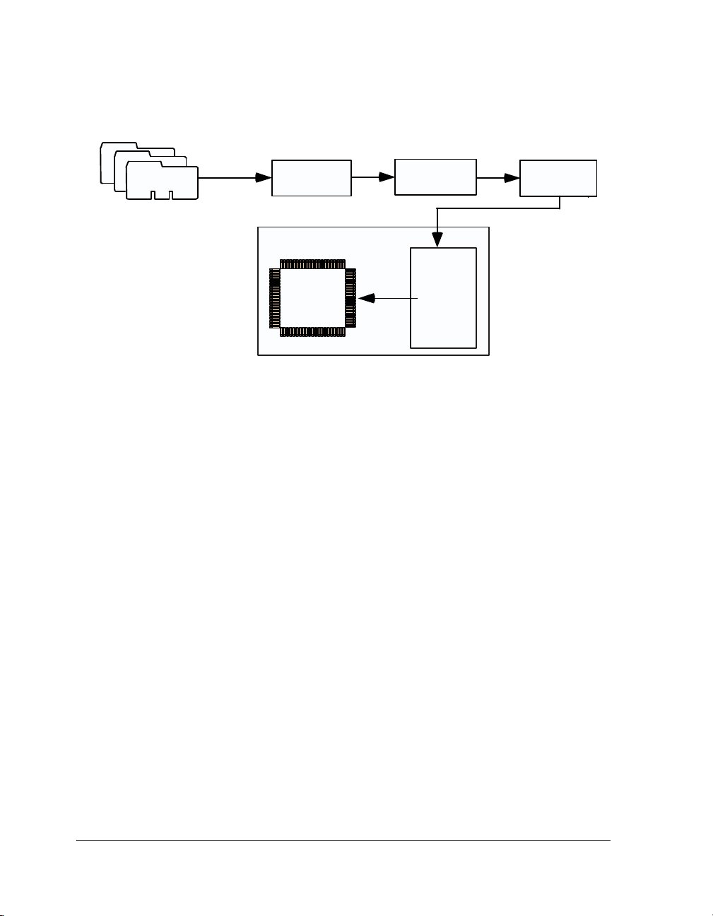
Program Development Flow
SOURCE
FILES
ASSEMBLER
AND/OR
COMPILER
.ASM , .C, .CPP
PROCESSOR
LOADER
AND/OR
SPLITTER
EXTERNAL
MEMORY
BOOTING
UPON
RESET
TARGET SYSTEM
.DOJ
.DXE
.LDR
LINKER
Figure 1-1. Program Development Flow
Compiling and Assembling
Input source files are compiled and assembled to yield object files. Source
files are text files containing C/C++ code, compiler directives, possibly a
mixture of assembly code and directives, and, typically, preprocessor commands. The assembler and compiler are documented in the
VisualDSP++ 5.0 Assembler and Preprocessor Manual and
VisualDSP++ 5.0 C/C++ Compiler and Library Manual, which are part of
the online help.
Linking
Under the direction of the linker description file (LDF) and linker settings, the linker consumes separately-assembled object and library files to
yield an executable file. If specified, the linker also produces the shared
memory files and overlay files. The linker output (
the ELF standard, an industry-standard format for executable files. The
linker also produces map files and other embedded information
(DWARF-2) used by the debugger.
1-8 VisualDSP++ 5.0 Loader and Utilities Manual
.dxe files) conforms to
Page 29

Introduction
These executable files are not readable by the processor hardware directly.
They are neither supposed to be burned onto an EPROM or flash memory
device. Executable files are intended for VisualDSP++ debugging targets,
such as the simulator or emulator. Refer to the VisualDSP++ 5.0 Linker
and Utilities Manual and online Help for information about linking and
debugging.
Loading, Splitting, or Both
Upon completing the debug cycle, the processor hardware needs to run on
its own, without any debugging tools connected. After power-up, the
processor’s on-chip and off-chip memories need to be initialized. The process of initializing memories is often referred to as booting. Therefore, the
linker output must be transformed to a format readable by the processor.
This process is handled by the loader and/or splitter utility. The
loader/splitter utility uses the debugged and tested executable files as well
as shared memory and overlay files as inputs to yield a processor-loadable
file.
VisualDSP++ 5.0 includes these loader and splitter utilities:
• elfloader.exe (loader utility) for Blackfin, TigerSHARC, and
SHARC processors. The loader utility for Blackfin processors also
acts as a ROM splitter utility when evoked with the corresponding
switches.
• elfspl21k.exe (ROM splitter utility) for TigerSHARC and
SHARC processors.
VisualDSP++ 5.0 Loader and Utilities Manual 1-9
Page 30

Program Development Flow
The loader/splitter output is either a boot-loadable or non-bootable file.
The output is meant to be loaded onto the target. There are several ways
to use the output:
• Download the loadable file into the processor’s PROM space on an
EZ-KIT Lite
VisualDSP++ Help for information on the Flash Programmer.
• Use VisualDSP++ to simulate booting in a simulator session (currently supported on the ADSP-21060, ADSP-21061,
ADSP-21065L, ADSP-21160, and ADSP-21161 processors). Load
the loader file and then reset the processor to debug the booting
routines. No hardware is required: just point to the location of the
loader file, letting the simulator to do the rest. You can step
through the boot kernel code as it brings the rest of the code into
memory.
• Store the loader file in an array for a multiprocessor system. A master (host) processor has the array in its memory, allowing a full
control to reset and load the file into the memory of a slave
processor.
®
board via the Flash Programmer plug-in. Refer to
Non-bootable Files Versus Boot-loadable Files
A non-bootable file executes from an external memory of the processor,
while a boot-loadable file is transported into and executes from an internal
memory of the processor. The boot-loadable file is then programmed into
an external memory device (burned into EPROM) within your target system. The loader utility outputs loadable files in formats readable by most
EPROM burners, such as Intel hex-32 and Motorola S formats. For
advanced usage, other file formats and boot modes are supported.
See “File Formats” on page A-1.
A non-bootable EPROM image file executes from an external memory of
the processor, bypassing the built-in boot mechanisms. Preparing a
non-bootable EPROM image is called splitting. In most cases (except for
1-10 VisualDSP++ 5.0 Loader and Utilities Manual
Page 31

Introduction
Blackfin processors), developers working with floating- and fixed-point
processors use the splitter instead of the loader utility to produce a
non-bootable memory image file.
A booting sequence of the processor and application program design dictate the way loader/splitter utility is called to consume and transform
executable files:
• For Blackfin processors, loader and splitter operations are handled
by the loader utility program,
elfloader.exe. The splitter is
invoked by a different set of command-line switches than the
loader.
In VisualDSP++ 5.0, with the addition of the -readall switch, the
loader utility for the ADSP-BF51x/BF52x/BF54x Blackfin processors can call the splitter program automatically. For more
information, see -readall #.
• For TigerSHARC and SHARC processors, splitter operations are
handled by the splitter program, elfspl21k.exe.
Loader Utility Operations
Common tasks performed by the loader utility can include:
• Processing the loader option settings or command-line switches.
• Formatting the output
.ldr file according to user specifications.
Supported formats are binary, ASCII, Intel hex-32, and more.
Valid file formats are described in “File Formats” on page A-1.
• Packing the code for a particular data format: 8-, 16- or 32-bit for
some processors.
• Adding the code and data from a specified initialization executable
file to the loader file, if applicable.
• Adding a boot kernel on top of the user code.
VisualDSP++ 5.0 Loader and Utilities Manual 1-11
Page 32

Program Development Flow
• If specified, preprogramming the location of the
.ldr file in a
specified PROM space.
• Specifying processor IDs for multiple input .dxe files for a
multiprocessor system, if applicable.
You can run the loader utility from the VisualDSP++ Integrated Development and Development Environment (IDDE), when the IDDE is
available, or from the command line. In order to do so in the IDDE, open
the Project Options dialog box from the Project menu, and change the
project’s target type from Executable file to Loader File.
Loader utility operations depend on the loader options, which control
how the loader utility processes executable files into boot-loadable files,
letting you select features such as kernels, boot modes, and output file formats. These options are set on the Load pages of the Project Options
dialog box in the IDDE or on the loader command line. Option settings
on the Load pages correspond to switches typed on the elfloader.exe
command line.
Splitter Utility Operations
Splitter utility operations depend on the splitter options, which control
how the splitter utility processes executable files into non-bootable files:
• For Blackfin processor, the loader utility includes the ROM splitter
capabilities invoked through the Project Options dialog box. Refer
to “Using VisualDSP++ ROM Splitter” on page 3-78. Option settings in the dialog box correspond to switches typed on the
elfloader.exe command line.
• For SHARC and TigerSHARC processors, change the project’s target type to Splitter file. The splitter options are set via the Project:
Split page of the Project Options dialog box. Refer to “Splitter for
1-12 VisualDSP++ 5.0 Loader and Utilities Manual
Page 33

Introduction
SHARC and TigerSHARC Processors” on page 8-1. Option set-
tings in the dialog box correspond to switches typed on the
elfspl21k.exe command line.
Boot Modes
Once an executable file is fully debugged, the loader utility is ready to
convert the executable file into a processor-loadable (boot-loadable) file.
The loadable file can be automatically downloaded (booted) to the processor after power-up or after a software reset. The way the loader utility
creates a boot-loadable file depends upon how the loadable file is booted
into the processor.
The boot mode of the processor is determined by sampling one or more of
the input flag pins. Booting sequences, highly processor-specific, are
detailed in the following chapters.
Analog Devices processors support different boot mechanisms. In general,
the following schemes can be used to provide program instructions to the
processors after reset.
• No-Boot Mode
• PROM Boot Mode
• Host Boot Mode
No-Boot Mode
After reset, the processor starts fetching and executing instructions from
EPROM/flash memory devices directly. This scheme does not require any
loader mechanism. It is up to the user program to initialize volatile
memories.
VisualDSP++ 5.0 Loader and Utilities Manual 1-13
Page 34

Boot Modes
The splitter utility generates a file that can be burned into the PROM
memory.
PROM Boot Mode
After reset, the processor starts reading data from a parallel or serial
PROM device. The PROM stores a formatted boot stream rather than raw
instruction code. Beside application data, the boot stream contains additional data, such as destination addresses and word counts. A small
program called a boot kernel (described on page 1-15) parses the boot
stream and initializes memories accordingly. The boot kernel runs on the
target processor. Depending on the architecture, the boot kernel may execute from on-chip boot RAM or may be preloaded from the PROM
device into on-chip SRAM and execute from there.
The loader utility generates the boot stream from the linker output (an
executable file) and stores it to file format that can be burned into the
PROM.
Host Boot Mode
In this scheme, the target processor is a slave to a host system. After reset,
the processor delays program execution until the slave gets signalled by the
host system that the boot process has completed. Depending on hardware
capabilities, there are two different methods of host booting. In the first
case, the host system has full control over all target memories. The host
halts the target while initializing all memories as required. In the second
case, the host communicates by a certain handshake with the boot kernel
running on the target processor. This kernel may execute from on-chip
ROM or may be preloaded by the host devices into the processor’s SRAM
by any bootstrapping scheme.
1-14 VisualDSP++ 5.0 Loader and Utilities Manual
Page 35

Introduction
The loader/splitter utility generates a file that can be consumed by the
host device. It depends on the intelligence of the host device and on the
target architecture whether the host expects raw application data or a formatted boot stream.
In this context, a boot-loadable file differs from a non-bootable file in that
it stores instruction code in a formatted manner in order to be processed
by a boot kernel. A non-bootable file stores raw instruction code.
Boot Kernels
A boot kernel refers to the resident program in the boot ROM space
responsible for booting the processor. Alternatively (or in absence of the
boot ROM), the boot kernel can be preloaded from the boot source by a
bootstrapping scheme.
When a reset signal is sent to the processor, the processor starts booting
from a PROM, host device, or through a communication port. For example, an ADSP-2106x/2116x processor, brings a 256-word program into
internal memory for execution. This small program is a boot kernel.
The boot kernel then brings the rest of the application code into the processor’s memory. Finally, the boot kernel overwrites itself with the final
block of application code and jumps to the beginning of the application
program.
Some of the newer Blackfin processors do not require to load a boot kernel—a kernel is already present in the on-chip boot ROM. It allows the
entire application program’s body to be booted into the internal and
external memories of the processor. The boot kernel in the on-chip ROM
behaves similar to the second-stage loader of the ADSP-BF535 processors.
The boot ROM has the capability to parse address and count information
for each bootable block.
VisualDSP++ 5.0 Loader and Utilities Manual 1-15
Page 36

Boot Streams
.LDR F ILE
CODE
DATA
SYMBOLS
DEBUG
INFORM ATION
.DXE FILE
CODE
DATA
SYMBOLS
DEBUG
INFORMATION
A .DXE FILE INCLUDES:
- DSP INSTRUCTIONS (CODE AND DATA)
- SYMBOL TABLE AND SECTION INFORMATION
- TARGET PROCESSOR MEMO RY LAYOUT
- DEBUG INFORMATION
AN .LDR FILE INCLUDES:
- DSP INSTRUCTIONS (CODE AND DATA)
- RUDIMENTARY FORMATT ING
(ALL DEBUG INFORMATION HAS
BEEN REMOVED)
Boot Streams
The loader utility’s output (.ldr file) is essentially the same executable
code as in the input .dxe file; the loader utility simply repackages the executable as shown in Figure 1-2.
Figure 1-2. A .dxe File Versus an .ldr File
Processor code and data in a loader file (also called a boot stream) is split
into blocks. Each code block is marked with a tag that contains information about the block, such as the number of words and destination in the
processor’s memory. Depending on the processor family, there can be
additional information in the tag. Common block types are “zero” (memory is filled with
Depending on the processor family, there can be other block types.
Refer to the following chapters to learn more about boot streams.
1-16 VisualDSP++ 5.0 Loader and Utilities Manual
0s); nonzero (code or data); and final (code or data).
Page 37

Introduction
File Searches
File searches are important in the loader utility operation. The loader utility supports relative and absolute directory names and default directories.
File searches occur as follows.
• Specified path—If relative or absolute path information is included
in a file name, the loader utility searches only in that location for
the file.
• Default directory—If path information is not included in the file
name, the loader utility searches for the file in the current working
directory.
• Overlay and shared memory files—The loader utility recognizes
overlay and shared memory files but does not expect these files on
the command line. Place the files in the directory that contains the
executable file that refers to them, or place them in the current
working directory. The loader utility can locate them when processing the executable file.
When providing an input or output file name as a loader/splitter command-line parameter, use these guidelines:
• Enclose long file names within straight quotes, “long file name”.
• Append the appropriate file extension to each file.
VisualDSP++ 5.0 Loader and Utilities Manual 1-17
Page 38

File Searches
1-18 VisualDSP++ 5.0 Loader and Utilities Manual
Page 39

2 LOADER/SPLITTER FOR
ADSP-BF51X/BF52X/BF54X
BLACKFIN PROCESSORS
This chapter explains how the loader/splitter utility (elfloader.exe) is
used to convert executable (.dxe) files into boot-loadable or non-bootable
files for the ADSP-BF51x, ADSP-BF52x, and ADSP-BF54x Blackfin
processors.
Refer to “Introduction” on page 1-1 for the loader utility overview.
Loader operations specific to the ADSP-BF51x/BF52x/BF54x Blackfin
processors are detailed in the following sections.
• “ADSP-BF51x/BF52x/BF54x Processor Booting” on page 2-2
Provides general information on various boot modes, including
information on second-stage kernels.
• “ADSP-BF51x/BF52x/BF54x Processor Loader Guide” on
page 2-5
Provides reference information on the loader utility’s command-line syntax and switches.
VisualDSP++ 5.0 Loader and Utilities Manual 2-1
Page 40

ADSP-BF51x/BF52x/BF54x Processor Booting
ADSP-BF51x/BF52x/BF54x Processor
Booting
Table 2-1 lists the part numbers that currently comprise the
ADSP-BF51x/BF52x/BF54x families of Blackfin processors. Future
releases of VisualDSP++ may support additional processors.
Upon reset, an ADSP-BF51x/BF52x/BF54x processor starts fetching and
executing instructions from the on-chip boot ROM at address
0xEF00 0000. The boot ROM is an on-chip read-only memory that holds
a boot kernel program to load data from an external memory or host
device. The boot ROM details can be found in the corresponding Blackfin
Processor Hardware Reference.
Table 2-1. ADSP-BF51x/BF52x/BF54x Part Numbers
Processor Family Part Numbers
ADSP-BF518 ADSP-BF512, ADSP-BF514, ADSP-BF516, ADSP-BF518
ADSP-BF526 ADSP-BF522, ADSP-BF524, ADSP-BF526
ADSP-BF527 ADSP-BF523, ADSP-BF525, ADSP-BF527
ADSP-BF548 ADSP-BF542, ADSP-BF544, ADSP-BF547, ADSP-BF548, ADSP-BF549
ADSP-BF548M ADSP-BF542M, ADSP-BF544M, ADSP-BF547M, ADSP-BF548M,
ADSP-BF549M
There are other boot modes available, including idle (no-boot) mode. The
processor transitions into the boot mode sequence configured by the
BMODE pins; see Table 2-2 and Table 2-3. The BMODE pins are dedicated
mode-control pins; that is, no other functions are performed by the pins.
The pins can be read through bits in the system configuration register
(SYSCR).
2-2 VisualDSP++ 5.0 Loader and Utilities Manual
Page 41

Loader/Splitter for ADSP-BF51x/BF52x/BF54x Blackfin Processors
There are two categories of boot modes: master and slave. In master boot
modes, the processor actively loads data from parallel or serial memory
devices. In slave boot modes, the processor receives data from parallel or
serial memory devices.
L
for more information on system configuration, peripherals, registers, and operating modes:
• Blackfin processor data sheets can be found at
Refer to the processor’s data sheet and hardware reference manual
http://www.analog.com/en/embedded-processing-dsp/blackfin/processors/data-sheets/resources/index.html
.
• Blackfin processor manuals can be found at
http://www.analog.com/en/embedded-processing-dsp/blackfin/processors/manuals/resources/index.html
.
Table 2-2. ADSP-BF51x Boot Modes
Boot Source BMODE[2:0] Start Address
Idle (no-boot) 000 N/A
Eight- or 16-bit external flash memory (default mode) 001 0x2000 0000
Internal SPI memory 010 0x2030 0000
External SPI memory (EEPROM or flash) 011 0x0000 0000
SPI0 host device 100 N/A
One-time programmable (OTP) memory 101 N/A
SDRAM memory
UART0 host 111 N/A
110 N/A
VisualDSP++ 5.0 Loader and Utilities Manual 2-3
Page 42

ADSP-BF51x/BF52x/BF54x Processor Booting
Table 2-3. ADSP-BF52x/BF54x Boot Modes
Boot Source BMODE[3:0] Start Address
Idle (no-boot) 0000 N/A
Eight- or 16-bit external flash memory (default mode) 0001 0x2000 0000
16-bit asynchronous FIFO 0010 0x2030 0000
Eight-, 16-, 24-, or 32-bit addressable SPI memory 0011 0x0000 0000
External SPI host device 0100 N/A
Serial TWI memory 0101 0x0000 0000
TWI host 0110 N/A
UART0 host on ADSP-BF52x processors;
UART1 host on ADSP-BF54x processors
UART1 host on ADSP-BF52x processors;
Reserved on ADSP-BF54x processors
Reserved 1001 N/A
SDRAM/DDR 1010 0x0000 0010
OTP memory 1011 default page
Eight- or 16-bit NAND flash memory 1100, 1101 0x0000 0000
16-bit host DMA 1110 N/A
Eight-bit host DMA 1111 N/A
0111 N/A
1000 N/A
0x40
2-4 VisualDSP++ 5.0 Loader and Utilities Manual
Page 43

Loader/Splitter for ADSP-BF51x/BF52x/BF54x Blackfin Processors
ADSP-BF51x/BF52x/BF54x Processor Loader Guide
The loader utility post processes VisualDSP++ executable (.dxe) files and
generates loader (.ldr) files. A loader file can be formatted as binary,
ASCII or Intel hex style. An .ldr file contains the boot stream in a format
expected by the on-chip boot kernel.
Loader utility operations depend on the loader options, which control
how the utility processes executable files. You select features such as boot
modes, boot kernels, and output file formats via the options. The options
are specified on the loader utility’s command line or via the Load page of
the Project Options dialog box in the VisualDSP++ environment. The
Load page consists of multiple panes. When you open the Load page, the
default loader settings for the selected processor are set already.
L
These sections describe how to produce a bootable (single and multiple)
or non-bootable loader file:
VisualDSP++ 5.0 Loader and Utilities Manual 2-5
Option settings on the Load page correspond to switches displayed
on the command line.
• “Using Blackfin Loader Command Line” on page 2-6
• “Using VisualDSP++ Loader” on page 2-18
• “Using VisualDSP++ Second-Stage Loader” on page 2-20
• “Using VisualDSP++ ROM Splitter” on page 2-22
Page 44

ADSP-BF51x/BF52x/BF54x Processor Loader Guide
Using Blackfin Loader Command Line
The ADSP-BF51x/BF52x/BF54x Blackfin loader utility uses the following
command-line syntax.
For a single input file:
elfloader inputfile -proc processor [-switch …]
For multiple input files:
elfloader inputfile1 inputfile2 … -proc processor [-switch …]
where:
• inputfile—Name of the executable (.dxe) file to be processed
into a single boot-loadable or non-bootable file. An input file name
can include the drive and directory. For multiprocessor or
multi-input systems, specify multiple input .dxe files. Put the
input file names in the order in which you want the loader utility
to process the files. Enclose long file names within straight quotes,
“long file name”.
• -proc processor—Part number of the processor (for example,
-proc ADSP-BF542) for which the loadable file is built. Provide a
processor part number for every input
cessor systems; see Table 2-1.
•
-switch …—One or more optional switches to process. Switches
select operations and modes for the loader utility.
L
2-6 VisualDSP++ 5.0 Loader and Utilities Manual
Command-line switches may be placed on the command line in
any order, except the order of input files for a multi-input system.
For a multi-input system, the loader utility processes the input files
in the order presented on the command line.
.dxe if designing multipro-
Page 45

Loader/Splitter for ADSP-BF51x/BF52x/BF54x Blackfin Processors
File Searches
File searches are important in loader processing. The loader utility supports relative and absolute directory names, default directories, and
user-selected directories for file search paths. File searches occur as
described on page 1-17.
File Extensions
Some loader switches take a file name as an optional parameter. Table 2-4
lists the expected file types, names, and extensions.
Table 2-4. File Extensions
Extension File Description
.dxe Loader input files, boot kernel files, and initialization files
.ldr Loader output file
.knl Loader output files containing kernel code only when two output files are selected
In some cases, the loader utility expects the overlay input files with the
.ovl file extension, shared memory input files with the .sm extension, or
both but does not expect those files to appear on a command line or on
the Load property page. The loader utility finds these files in the directory
of the associated
directory specified in the
.dxe files, in the current working directory, or in the
.ldf file.
VisualDSP++ 5.0 Loader and Utilities Manual 2-7
Page 46

ADSP-BF51x/BF52x/BF54x Processor Loader Guide
ADSP-BF51x/BF52x/BF54x Blackfin Loader Command-Line Switches
A summary of the ADSP-BF51x/BF52x/BF54x Blackfin loader command-line switches appears in Table 2-5. For a quick on-line help on the
switches available for a specific processor; for example an ADSP-BF548
processor, use the following command line.
elfloader -proc ADSP-BF548 -help
Table 2-5. ADSP-BF51x/BF52x/BF54x Loader Command-Line Switch
Summary
Switch Description
-b flash
-b prom
-b spimaster
-b spislave
-b TWImaster
-b TWIslave
-b UART
-b FIFO
-b OTP
-b NAND
-CRC32 [polynomial] The -CRC32 (polynomial coefficient) switch directs the loader
The -b {prom|flash|spimaster|spislave|UART|TWImas-
ter|TWIslave|FIFO|OTP|NAND} switch directs the loader utility
to prepare a boot-loadable file for the specified boot mode. Valid
boot modes include flash, PROM, SPI master, SPI slave, UART,
TWI master, TWI slave, FIFO, OTP, NAND, and
SDRAM/DDR.
-b does not appear on the command line, the default is
If
-b flash.
utility to generate CRC32 checksum. Use a polynomial coefficient
if specified; otherwise, use default 0xD8018001.
This switch inserts an initcode boot block that calls an initialization routine residing in the on-chip boot ROM. The argument
field of the boot block provides the used polynomial. The loader
utility calculates the CRC checksum for all subsequent data blocks
and stores the result in the block header’s argument field.
L
The CRC32 checksum is not performed by the
ADSP-BF52x boot kernel.
2-8 VisualDSP++ 5.0 Loader and Utilities Manual
Page 47

Loader/Splitter for ADSP-BF51x/BF52x/BF54x Blackfin Processors
Table 2-5. ADSP-BF51x/BF52x/BF54x Loader Command-Line Switch
Summary (Cont’d)
Switch Description
-callback sym=symbol
[arg=const32]
The -callback switch takes a sym=symbol (no spaces) assignment.
The switch directs the loader utility to isolate the named subroutine into a separate block, set the block header’s
flag, and fill in the block header’s argument field with the specified
constant 32-bit values. The switch is used for boot-time callbacks.
The callback is guaranteed to be made prior to the target address
sym=symbol.
of
The -callback cannot be used with -CRC32.
BFLAG_CALLBACK
L
-dmawidth # The -dmawidth {8|16|32}switch specifies a DMA width (in
bits) for memory boot modes. It controls the
issued to the boot block headers by the -width switch.
For FIFO boot mode, 16 is the only DMA width. SPI, TWI, and
UART modes use 8-bit DMA.
-f hex
-f ASCII
-f binary
-f include
-h or -help The -help switch invokes the command-line help, outputs a list
The -f {hex|ASCII|binary|include} switch specifies the format of a boot-loadable file: Intel hex-32, ASCII, binary, or
include. If the -f switch does not appear on the command line,
the default file format is hex for flash/PROM boot modes; and
ASCII for other boot modes.
of command-line switches to standard output, and exits. By
default, the
obtain a help screen for your target Blackfin processor, add the
-proc switch to the command line. For example, type
elfloader -proc ADSP-BF542 -h to obtain help for the
ADSP-BF542 processor.
-h switch alone provides help for the loader driver. To
DMACODE bit field
VisualDSP++ 5.0 Loader and Utilities Manual 2-9
Page 48

ADSP-BF51x/BF52x/BF54x Processor Loader Guide
Table 2-5. ADSP-BF51x/BF52x/BF54x Loader Command-Line Switch
Summary (Cont’d)
Switch Description
-init filename.dxe The -init filename.dxe switch directs the loader utility to
include the initialization code from the named executable file. The
loader utility places the code and data from the initialization sections at the top of the boot stream. The boot kernel loads the code
and then calls it. It is the code’s responsibility to save/restore
state/registers and then perform an RTS back to the kernel. Initcodes can be written in C language and are compliant to C calling
conventions.
-init filename.dxe switch can be used multiple times to
The
specify the same file or different files a number of times. The
loader utility will place the code from the initialization files in the
order the files appear on the command line.
For more information, see “ADSP-BF51x/BF52x/BF54x
Multi-DXE Loader Files” on page 2-17.
2-10 VisualDSP++ 5.0 Loader and Utilities Manual
Page 49

Loader/Splitter for ADSP-BF51x/BF52x/BF54x Blackfin Processors
Table 2-5. ADSP-BF51x/BF52x/BF54x Loader Command-Line Switch
Summary (Cont’d)
Switch Description
-initcall sym=sym_symbol
at=at_symbol
[stride=DstAddrGap
count=times]
While the -init filename.dxe switch integrates initialization
codes managed by a separate application program, the -initcall
switch controls calls to initialization subroutines that are part of
the same application.
-initcall switch directs the loader utility to dispatch a
The
boot-time initialization call to the
sym subroutine when the at
symbol is encountered and loaded. The stride and count parameters are optional:
• If an optional
stride= constant 32-bit value is specified,
the loader utility insets the target program call every
stride= target address locations.
• If an optional
count= constant 32-bit value is specified,
the loader utility insets the target program call count=
times, every stride= target address locations apart. A
count value without a stride value is an error.
For example, the following command line
-initcall sym=_initcode at=_othersymbol
stride=0x100 count=5
results in function _initcode being called five times the first
time, just prior to data in
_othersymbol being booted. Thereaf-
ter, every 256 destination load addresses _initcode is called again
until a total of five calls have been made.
-initcall restrictions:
-initcall target (sym_symbol) must be a routine entry
•
point, end with an RTS. It can be written in C language
and can rely on the presence of a stack. However, the
routine must not call any libraries, not rely on compiler
run-time environment (such as heaps) – must be
self-contained
-initcall subroutine must be previously loaded and
•
still in memory
-initcall subroutine cannot contain any forward refer-
•
ences to code not yet loaded
sym_symbol address must be less than at_symbol
•
address
For more information, see “ADSP-BF51x/BF52x/BF54x
Multi-DXE Loader Files” on page 2-17.
VisualDSP++ 5.0 Loader and Utilities Manual 2-11
Page 50

ADSP-BF51x/BF52x/BF54x Processor Loader Guide
Table 2-5. ADSP-BF51x/BF52x/BF54x Loader Command-Line Switch
Summary (Cont’d)
Switch Description
-kb flash
-kb prom
-kb spimaster
-kb spislave
-kb UART
-kb TWImaster
-kb TWIslave
-kb FIFO
-kb otp
-kb nand
-kf hex
-kf ascii
-kf binary
-kf include
-kp # The -kp # switch specifies a hex flash/PROM start address for the
The -kb {flash|prom|spimaster|spislave|UART|TWImas-
ter|TWIslave|FIFO|otp|nand} switch specifies the boot mode:
flash, PROM, SPI master, SPI slave, UART, TWI master, TWI
slave, or FIFO, OTP, NAND, and SDRAM/DDR. for the initialization code and/or boot kernel output file if two output loader
files are selected.
L
If the -kb switch is absent from the command line, the loader utility generates the file for the init and/or boot kernel code in the
same boot mode as used to output the user application program.
The -kf {hex|ascii|binary|include} switch specifies the
output file format (hex, ASCII, binary, include) for the initialization and/or boot kernel code if two output files from the loader
utility are selected: one file for the init code and/or boot kernel
and one file for user application code.
L
-kf is absent from the command line, the loader utility gener-
If
ates the file for the initialization and /or boot kernel code in the
same format as for the user application code.
initialization and/or boot kernel code. A valid value is between
0x0 and 0xFFFFFFFF. The specified value is ignored when neither
kernel nor initialization code is included in the loader file.
The -kb switch must be used in conjunction with
-o2 switch.
the
The -kf switch must be used in conjunction with
the -o2 switch.
2-12 VisualDSP++ 5.0 Loader and Utilities Manual
Page 51

Loader/Splitter for ADSP-BF51x/BF52x/BF54x Blackfin Processors
Table 2-5. ADSP-BF51x/BF52x/BF54x Loader Command-Line Switch
Summary (Cont’d)
Switch Description
-kwidth # The -kwidth {8|16|32} switch specifies an external memory
device width (in bits) for the initialization code and/or the boot
kernel if two output files from the loader utility are selected.
-kwidth is absent from the command line, the loader utility
If
generates the boot kernel file in the same width as the user application program.
L
-l userkernel.dxe The -l userkernel.dxe switch specifies the user boot kernel file.
L
-M The -M switch generates make dependencies only, no output file is
generated.
-maskaddr # The -maskaddr # switch masks all EPROM address bits above or
equal to #. For example, -maskaddr 29 (default) masks all the
bits above and including A29 (ANDed by 0x1FFF FFFF). For exam-
0x2000 0000 becomes 0x0000 0000. The valid #s are inte-
ple,
gers 0 through 32, but based on your specific input file, the value
can be within a subset of [0, 32].
L
-MaxBlockSize # The -MaxBlockSize # switch specifies the maximum block size
up to
0x7FFFFFF0. The value must be a multiple of 4.
The default maximum block size is
by the
The -kWidth # switch must be used in conjunction
with the
There is no default kernel for the
ADSP-BF51x/BF52x/BF54x processors.
The -maskaddr # switch requires -romsplitter
and affects the ROM section address only.
-MaxBlockSize switch.
-o2 switch.
0xFFF0 or the value specified
-MaxFillBlockSize # The -MaxFillBlockSize # switch specifies the maximum fill
block size up to
The default fill block size is
0xFFFFFF0. The value must be a multiple of two.
0xFFF0.
VisualDSP++ 5.0 Loader and Utilities Manual 2-13
Page 52

ADSP-BF51x/BF52x/BF54x Processor Loader Guide
Table 2-5. ADSP-BF51x/BF52x/BF54x Loader Command-Line Switch
Summary (Cont’d)
Switch Description
-MM The -MM switch generates make dependencies while producing the
output files.
-Mo filename The -Mo filename switch writes make dependencies to the named
file. Use the
default is a <stdout> display.
-Mt target The -Mt target switch specifies the make dependencies target
output file. Use the -Mt switch with either -M or -MM. If -Mt is not
present, the default is the name of the input file with an
extension.
-NoInitCode The -NoInitCode switch directs the loader utility not to expect
an init code file. The loader utility may expect an init code file,
specified through the
tion has an external memory section. The init code file should
contain the code to initialize registers for external memory initialization.
-Mo switch with either -M or -MM. If -Mo is absent, the
.ldr
-init filename.dxe switch if the applica-
-o filename The -o filename switch directs the loader utility to use the speci-
fied file as the name of the loader utility’s output file. If the file-
name is absent, the default name is the root name of the input file
with an
-o2 The -o2 switch directs the loader utility to produce two output
files: one file for code from the initialization block and/or boot
kernel and one file for user application code.
To have a different format, boot mode, or output width for the
application code output file, use the
to specify the boot mode, the boot format, and the boot width for
the output kernel file, respectively.
-p # The -p # switch specifies a hex flash/PROM output start address
for the application code. A valid value is between
0xFFFFFFFF. A specified value must be greater than that specified
by
in the same output file (a single output file).
.ldr extension.
-kb -kf -kwidth switches
L
-kp if both kernel and/or initialization and application code are
Combine -o2 with -l filename and/or -init
filename.dxe.
0x0 and
2-14 VisualDSP++ 5.0 Loader and Utilities Manual
Page 53

Loader/Splitter for ADSP-BF51x/BF52x/BF54x Blackfin Processors
Table 2-5. ADSP-BF51x/BF52x/BF54x Loader Command-Line Switch
Summary (Cont’d)
Switch Description
-proc processor The -proc processor switch specifies the target processor.
The processor can be one of the processors listed in Table 2-1.
-quickboot sec=section The -quickboot switch takes a sec=section (no spaces) assign-
ment.
The switch directs the loader utility to mark blocks within the
LDF-defined output section name with the
flag. The switch is used to mark blocks to skip on warm-boot
cycles.
-readall # The -readall # switch directs the loader utility to integrate
fixed-position ROM sections within the loader boot stream. The
switch calls the splitter utility as a transparent sub-process to the
loader utility. Memory segments declared with the
command in the LDF file are processed by the splitter. Segments
with the
TYPE(RAM) command emit to the boot stream.
The valid switch argument is an integer between 0 and 32, where
29 is the default. In the resulting loader (.ldr) file in Intel hex-32
format, the ROM-based splitter data is merged with the
RAM-based loader stream.
# argument is similar to the -maskaddr # switch, which desig-
The
nates the upper PROM address bit position for extended address
mapping. The splitter utility is required to provide the -maskaddr
# parameter to the loader utility to generate a ROM-based splitter
stream, but the required splitter parameter is not available on the
loader command line. The loader utility solves this requirement by
supporting the
-readall # switch.
BFLAG_QUICKBOOT
TYPE(ROM)
-romsplitter The -romsplitter switch creates a non-bootable image only.
This switch overwrites the
-b switch and any other switch
bounded by the boot mode.
.ldf file, declare memory segments to be ‘split’ as type ROM.
In the
The splitter skips
segments are declared as
RAM segments, resulting in an empty file if all
RAM. The -romsplitter switch supports
Intel hex and ASCII formats.
VisualDSP++ 5.0 Loader and Utilities Manual 2-15
Page 54

ADSP-BF51x/BF52x/BF54x Processor Loader Guide
Table 2-5. ADSP-BF51x/BF52x/BF54x Loader Command-Line Switch
Summary (Cont’d)
Switch Description
-save [sec=section] The -save switch takes a sec=section (no spaces) assignment.
The switch directs the loader utility to mark blocks within the
LDF-defined section name with the
is used to mark blocks to archive for low-power or power-fail
cycles.
-si-revision #.#|none|any The -si-revision {#.#|none|any} switch provides a silicon
revision of the specified processor. The switch parameter represents a silicon revision of the processor specified by the
processor switch. The parameter takes one of three forms:
•The
•The
•The any value indicates that VisualDSP++ produces an
The switch generates either a warning about any potential anomalous conditions or an error if any anomalous conditions occur.
#.# value indicates one or more decimal digits, fol-
lowed by a point, followed by one or two decimal digits.
Examples of revisions are: 0.0; 1.12; 23.1. Revision 0.0
is default. Revision
revision 0.10. The digits to the left of the point specify
the chip tapeout number; the digits to the right of the
point identify the metal mask revision number. The
number to the right of the point cannot exceed decimal
255.
none value indicates that the VisualDSP++ ignores
silicon errata.
output file that can be run at any silicon revision.
BFLAG_SAVE flag. The switch
-proc
0.1 is distinct from and “lower” than
[
-v The -v switch directs the loader utility to output verbose loader
messages and status information as the loader processes files.
-width # The -width {8|16|32} switch specifies an external memory
device width (in bits) to the loader utility in flash/PROM boot
mode (default is eight). For FIFO boot mode, the only valid width
16. For SPI, TWI, and UART boot modes, the only valid width
is
is eight.
In the absence of the silicon revision switch, the
loader utility selects the default silicon revision it is
aware of, if any.
2-16 VisualDSP++ 5.0 Loader and Utilities Manual
Page 55

Loader/Splitter for ADSP-BF51x/BF52x/BF54x Blackfin Processors
ADSP-BF51x/BF52x/BF54x Multi-DXE Loader Files
An ADSP-BF51x/BF52x/BF54x loader (
.ldr) file can contain data of
multiple application (.dxe) files. At boot time, the boot kernel boots one
application file exclusively, or one application file initiates the boot of the
next application file. In some cases, a single application can consist of
multiple .dxe files.
Initialization code is a subroutine called at boot time. Unlike the
ADSP-BF53x/BF56x processors, the ADSP-BF51x/BF52x/BF54x processors support initcode written in both assembly and C.
VisualDSP++ supports two methods of integrating multiple initcode
subroutines:
• The -init filename.dxe command-line switch expects a .dxe file.
The initcode is managed by a separate VisualDSP++ project. If the
initcode is written in C language, ensure that the .dxe file does not
include the CRT code because the boot kernel expects a subroutine.
The -init filename.dxe switch can be used multiple times to specify
the same file or different files a number of times. The loader utility
places the code from the initialization files in the order the files
appear on the command line. All initcodes are inserted after the
first regular
.dxe file.
The loader utility equips every initcode with a dedicated first boot
block, which has the BFLAG_FIRST flag set. Initcodes, however, do
not feature a final block; they are terminated by a boot block,
VisualDSP++ 5.0 Loader and Utilities Manual 2-17
Page 56

ADSP-BF51x/BF52x/BF54x Processor Loader Guide
tagged by the
BFLAG_FINAL flag, the boot kernel continues processing of the sub-
BFLAG_INIT flag. Therefore, in absence of the
sequent .dxe data after finishing execution of the initcode.
• The -initcall sym=sym_symbol command-line switch relies on init-
code subroutines that are part of the same VisualDSP++ project.
Initcode subroutines invoked by the –initcall switch are not
accompanied by any first boot blocks with the BFLAG_FIRST flag
set. In the loader file, the initcode subroutines translate to boot
blocks tagged by the BFLAG_INIT flag.
When writing an initcode subroutine in C, ensure that the code does not
rely on libraries or heap support, which may not be available in memory
by the time the initcode executes. An initcode routine is expected to
return properly to the boot kernel by an RTS instruction and to meet
C-language calling conventions (see the VisualDSP++ 5.0 C/C++
Compiler and Library Manual for Blackfin Processors).
Refer to the initcode examples provided with the VisualDSP++ installation in <install_path>\Blackfin\ldr\init_code.
Using VisualDSP++ Loader
After selecting a Loader file (.ldr) as the project output type for your
Blackfin application on the Application Settings page in the VisualDSP++
Project Wizard, modify the default load settings.
The Load control in the Project tree control consists of multiple pages.
When you open the Load: Options page (also called loader property page),
view the default load settings for the selected processor. As an example,
Figure 2-1 shows the ADSP-BF548 processor’s default load settings for
PROM boot mode. The dialog box options are equivalent to the command-line switches. Refer to “ADSP-BF51x/BF52x/BF54x Blackfin
Loader Command-Line Switches” on page 2-8 for more information
about the switches.
2-18 VisualDSP++ 5.0 Loader and Utilities Manual
Page 57

Loader/Splitter for ADSP-BF51x/BF52x/BF54x Blackfin Processors
Figure 2-1. Project: Load: Options Page for ADSP-BF548 Processors
Using the page controls, select or modify the load settings. Table 2-6
describes each load control and corresponding setting. When satisfied
with the settings, click OK to complete the load setup.
Table 2-6. Base Load Page Settings for ADSP-BF51x/BF52x/BF54x
Processors
Setting Description
Load Selections for the loader utility. The selections are:
• Options – default boot options (this section)
• Kernel – specification for a second-stage loader (see page 2-20)
• Splitter – specification for the no-boot mode (see page 2-22)
Boot mode Specifies flash/PROM, SPI, SPI slave, UART, TWI, FIFO,
SDRAM/DDR, OTP, or NAND as a boot source.
VisualDSP++ 5.0 Loader and Utilities Manual 2-19
Page 58

ADSP-BF51x/BF52x/BF54x Processor Loader Guide
Table 2-6. Base Load Page Settings for ADSP-BF51x/BF52x/BF54x
Processors (Cont’d)
Setting Description
Boot format Specifies Intel hex, ASCII, include, or binary format.
Output width Specifies eight or 16 bits.
Use default start
address
Start address Specifies a flash/PROM output start address in hex format for the appli-
Verbose Generates status information as the loader utility processes the files.
Initialization file Directs the loader utility to include the initialization file (init code).
Output file Names the loader utility’s output file.
Additional options Specifies additional loader switches. You can specify additional input
Uses the default flash/PROM output start address in hex format for the
application code.
cation code.
files for a multi-input system. Type the input file names with the paths
if the files are not in the current working directory, separate any two file
names with a space in order for the loader utility to retrieve the files.
Note: The loader utility processes the input files in the order in which
the files appear on the command line, generated from the property page.
Using VisualDSP++ Second-Stage Loader
If you use a second-stage loader, select Kernel under Load in the Project
Options tree control. The page shows the default settings for a loader file
that does not include a second-stage loader.
Unless you develop a second-stage loader and use it, most of the options
on the Kernel page are grayed out. Figure 2-2 shows a sample Kernel page
with options set for an ADSP-BF548 Blackfin processor.
2-20 VisualDSP++ 5.0 Loader and Utilities Manual
Page 59

Loader/Splitter for ADSP-BF51x/BF52x/BF54x Blackfin Processors
Figure 2-2. Project: Load: Kernel Page for ADSP-BF548 Processors
To create a loader file which includes a second-stage loader:
1. Select Options (under Load) to set up base load options
(see “Using VisualDSP++ Loader” on page 2-18).
2. Select Kernel (under Load) to set up the second-stage loader
options (Figure 2-2).
3. On the Kernel page, select Use boot kernel.
4. In Kernel file, enter the name of the second-stage loader file
(.dxe).
VisualDSP++ 5.0 Loader and Utilities Manual 2-21
Page 60

ADSP-BF51x/BF52x/BF54x Processor Loader Guide
5. To produce two output files, select the Output kernel in separate
file check box. This option allows to boot the second-stage loader
with an initialization code (if any) from one source and the application code from another source. You can specify the kernel output
file options, such as the Boot Mode (source), Boot Format, and
Output Width.
6. Select Change hex output kernel code start address to specify the
Start address in hex format for the second-stage loader code. This
option allows you to place the second-stage loader file at a specific
location within the flash/PROM.
7. Click OK to complete the loader utility setup.
Using VisualDSP++ ROM Splitter
Unlike the loader utility, the splitter utility does not format the application data when transforming a .dxe file to an .ldr file. The splitter utility
emits raw data only. Whether data and/or instruction sections are processed by the loader or by the splitter utility depends upon the LDF’s
TYPE() command. Sections declared with TYPE(RAM) are consumed by the
loader utility, and sections declared by TYPE(ROM) are consumed by the
splitter.
Figure 2-3 shows a sample Load: Splitter page with ROM splitter options.
With the Enable ROM splitter box unchecked, only
are processed and all
TYPE(ROM) sections are ignored by the loader utility.
TYPE(RAM) segments
If the box is checked, TYPE(RAM) sections are ignored, and TYPE(ROM) segments are processed by the splitter utility.
The Mask Address field masks all EPROM address bits above or equal to
the number specified. For example, Mask Address = 29 (default) masks all
bits above and including
becomes
0x0000 0000. The valid numbers are integers 0 through 32; based
A29 (ANDed by 0x1FFF FFFF). Thus, 0x2000 0000
on your specific input file, the value can be within a subset of [0, 32].
2-22 VisualDSP++ 5.0 Loader and Utilities Manual
Page 61

Loader/Splitter for ADSP-BF51x/BF52x/BF54x Blackfin Processors
Figure 2-3. Project: Splitter Page for ADSP-BF548 Processors
VisualDSP++ 5.0 Loader and Utilities Manual 2-23
Page 62

ADSP-BF51x/BF52x/BF54x Processor Loader Guide
2-24 VisualDSP++ 5.0 Loader and Utilities Manual
Page 63

3 LOADER/SPLITTER FOR
ADSP-BF53X/BF561
BLACKFIN PROCESSORS
This chapter explains how the loader/splitter utility (elfloader.exe) is
used to convert executable (.dxe) files into boot-loadable or non-bootable
files for the ADSP-BF53x and ADSP-BF561 Blackfin processors.
Refer to “Introduction” on page 1-1 for the loader utility overview.
Loader operations specific to the ADSP-BF53x and ADSP-BF561 Blackfin processors are detailed in the following sections.
• “ADSP-BF53x/BF561 Processor Booting” on page 3-2
Provides general information on various boot modes, including
information on the second-stage kernels.
• “ADSP-BF53x/BF561 Processor Loader Guide” on page 3-57
Provides reference information on the loader utility’s command-line syntax and switches.
VisualDSP++ 5.0 Loader and Utilities Manual 3-1
Page 64

ADSP-BF53x/BF561 Processor Booting
ADSP-BF53x/BF561 Processor Booting
At power-up, after a reset, the processor transitions into a boot mode
sequence configured by the BMODE pins. The BMODE pins are dedicated
mode-control pins; that is, no other functions are performed by these
pins. The pins can be read through bits in the system reset configuration
register SYSCR.
An ADSP-BF53x or an ADSP-BF561 Blackfin processor can be booted
from an eight- or 16-bit flash/PROM memory or from an eight-,16-, or
24-bit addressable SPI memory. The ADSP-BF561 processors does not
support 24-bit addressable SPI memory boot. There is also a no-boot
option (bypass mode) in which execution occurs from a 16-bit external
memory.
• ADSP-BF531/BF532/BF533/BF534/BF536/BF537/
BF538/BF539 Processor Booting description is on page 3-3
• ADSP-BF535 Processor Booting description is on page 3-21
• ADSP-BF561 Processor Booting description is on page 3-35
Software developers who use the loader utility should be familiar with the
the following operations.
• “ADSP-BF53x and ADSP-BF561 Multi-Application (Multi-DXE)
Management” on page 3-46
• “ADSP-BF531/BF532/BF533/BF534/BF536/BF537 Processor
Compression Support” on page 3-49
3-2 VisualDSP++ 5.0 Loader and Utilities Manual
Page 65

Loader/Splitter for ADSP-BF53x/BF561 Blackfin Processors
ADSP-BF531/BF532/BF533/BF534/BF536/BF537/ BF538/BF539 Processor Booting
Upon reset, an ADSP-BF531/BF532/BF533/BF534/BF536/BF537/
BF538/BF539 processor jumps to the on-chip boot ROM or jumps to
16-bit external memory for execution (if BMODE = 0) located at
0x2000 0000. The
ADSP-BF531/BF532/BF533/BF534/BF536/BF537/BF538/BF539 Processor On-Chip Boot ROM details can be found on page 3-23.
Table 3-1 summarizes the boot modes and execution start addresses for
the ADSP-BF531, ADSP-BF532, ADSP-BF533, ADSP-BF538, and
ADSP-BF539 processors.
Table 3-2 summarizes the boot modes for the
ADSP-BF534/BF536/BF537 processors, which in addition to all of the
ADSP-BF531/BF532/BF533 processor boot modes, also can boot from a
TWI serial device, a TWI host, and a UART host.
VisualDSP++ 5.0 Loader and Utilities Manual 3-3
Page 66

ADSP-BF53x/BF561 Processor Booting
Table 3-1. Boot Mode Selections for ADSP-BF531/BF532/
BF533/BF538/BF539 Processors
Boot Source BMODE[1:0] Execution Start Address
ADSP-BF531
ADSP-BF532
Executes from a 16-bit external ASYNC
bank 0 memory (no-boot mode); see
on page 3-16
Eight- or 16-bit flash/PROM 01 0xFFA0 8000 0xFFA0 0000
SPI host in SPI slave mode 10 0xFFA0 8000 0xFFA0 0000
Eight-, 16-, or 24-bit addressable SPI memory
in SPI master boot mode with support for
Atmel AT45DB041B, AT45DB081B, and
AT45DB161B DataFlash devices
00 0x2000 0000 0x2000 0000
11 0xFFA0 8000 0xFFA0 0000
ADSP-BF533
ADSP-BF538
ADSP-BF539
Table 3-2. ADSP-BF534/BF536/BF537 Processor Boot Modes
Boot Source BMODE[2:0]
Executes from an external 16-bit memory connected to
ASYNC bank 0; (no-boot mode or bypass on-chip boot
ROM); see on page 3-16
Eight- or 16-bit flash/PROM 001
Reserved 010
000
Eight-, 16-, or 24-bit addressable SPI memory in SPI master
mode with support for Atmel AT45DB041B, AT45DB081B,
and AT45DB161B DataFlash devices
SPI host in SPI slave mode 100
TWI serial device 101
TWI host 110
UART host 111
011
3-4 VisualDSP++ 5.0 Loader and Utilities Manual
Page 67

Loader/Splitter for ADSP-BF53x/BF561 Blackfin Processors
• Execute from 16-bit external memory – execution starts from
address
0x2000 0000 with 16-bit packing. The boot ROM is
bypassed in this mode. All configuration settings are set for the
slowest device possible (3-cycle hold time; 15-cycle R/W access
times; 4-cycle setup).
• Boot from eight-bit or 16-bit external flash memory – the eight-bit
or 16-bit flash boot routine located in boot ROM memory space is
set up using asynchronous memory bank 0. All configuration settings are set for the slowest device possible (3-cycle hold time;
15-cycle R/W access times; 4-cycle setup). The boot ROM evaluates the first byte of the boot stream at address 0x2000 0000. If it is
0x40, eight-bit boot is performed. A 0x60 byte assumes a 16-bit
memory device and performs eight-bit DMA. A 0x20 byte also
assumes 16-bit memory but performs 16-bit DMA.
• Boot from serial SPI memory (EEPROM or flash) – eight-, 16-, or
24-bit addressable devices are supported as well as AT45DB041,
AT45DB081, AT45DB161, AT45DB321, AT45DB642, and
AT45DB1282 DataFlash® devices from Atmel. The SPI uses the
PF10/SPI SSEL1 output pin to select a single SPI EEPROM/flash
device, submits a read command and successive address bytes
(0x00) until a valid eight-, 16-, or 24-bit, or Atmel addressable
device is detected, and begins clocking data into the processor.
• Boot from SPI host device – the Blackfin processor operates in SPI
slave mode and is configured to receive the bytes of the
.ldr file
from an SPI host (master) agent. To hold off the host device from
transmitting while the boot ROM is busy, the Blackfin processor
asserts a
GPIO pin, called host wait (HWAIT), to signal the host device
not to send any more bytes until the flag is deasserted. The flag is
chosen by the user and this information is transferred to the Blackfin processor via bits 10:5 of the FLAG header.
VisualDSP++ 5.0 Loader and Utilities Manual 3-5
Page 68

ADSP-BF53x/BF561 Processor Booting
• Boot from UART – using an autobaud handshake sequence, a
boot-stream-formatted program is downloaded by the host. The
host agent selects a baud rate within the UART’s clocking capabilities. When performing the autobaud, the UART expects an “
(boot stream) character (eight bits data, 1 start bit, 1 stop bit, no
parity bit) on the RXD pin to determine the bit rate. It then replies
with an acknowledgement that is composed of 4 bytes: 0xBF, the
value of UART_DLL, the value of UART_DLH, and 0x00. The host can
then download the boot stream. When the processor needs to hold
off the host, it deasserts CTS. Therefore, the host must monitor this
signal.
• Boot from serial TWI memory (EEPROM/flash) – the Blackfin
processor operates in master mode and selects the TWI slave with
the unique ID 0xA0. It submits successive read commands to the
memory device starting at two byte internal address 0x0000 and
begins clocking data into the processor. The TWI memory device
should comply with Philips I2C Bus Specification version 2.1 and
have the capability to auto-increment its internal address counter
such that the contents of the memory device can be read
sequentially.
@”
• Boot from TWI host – the TWI host agent selects the slave with
the unique ID 0x5F. The processor replies with an acknowledgement, and the host can then download the boot stream. The TWI
2
host agent should comply with Philips I
C Bus Specification version 2.1. An I2C multiplexer can be used to select one processor at
a time when booting multiple processors from a single TWI.
To augment the boot modes, a secondary software loader can be added to
provide additional booting mechanisms. The secondary loader could provide the capability to boot from flash, variable baud rate, and other
sources.
3-6 VisualDSP++ 5.0 Loader and Utilities Manual
Page 69

Loader/Splitter for ADSP-BF53x/BF561 Blackfin Processors
The following loader topics also are discussed in this chapter.
• “ADSP-BF531/BF532/BF533/BF534/BF536/BF537/BF538/
BF539 Processor Boot Streams” on page 3-9
• “ADSP-BF531/BF532/BF533/BF534/BF536/BF537/BF538/
BF539 Processor Memory Ranges” on page 3-19
L
for more information on system configuration, peripherals, registers, and operating modes:
• Blackfin processor data sheets can be found at
Refer to the processor’s data sheet and hardware reference manual
http://www.analog.com/en/embedded-processing-dsp/blackfin/processors/data-sheets/resources/index.html.
• Blackfin processor manuals can be found at
http://www.analog.com/en/embedded-processing-dsp/blackfin/processors/manuals/resources/index.html.
ADSP-BF531/BF532/BF533/BF534/BF536/BF537/BF538/BF539 Processor On-Chip Boot ROM
The on-chip boot ROM for the ADSP-BF531/BF532/BF533/BF534/
BF536/BF537/BF538/BF539 processors does the following.
1. Sets up supervisor mode by exiting the
RESET interrupt service
routine and jumping into the lowest priority interrupt (IVG15).
Note that the on-chip boot ROM of the ADSP-BF534/BF536 and
ADSP-BF537 processors executes at the Reset priority level, does
not degrade to the lowest priority interrupt.
2. Checks whether the
RESET was a software reset and, if so, whether
to skip the entire sequence and jump to the start of L1 memory
0xFFA0 0000 for the ADSP-BF533/BF534/BF536/BF537/BF538
(
and ADSP-BF539 processors;
0xFFA0 8000 for the
VisualDSP++ 5.0 Loader and Utilities Manual 3-7
Page 70

ADSP-BF53x/BF561 Processor Booting
ADSP -BF53 1/32/33/34/36/37/39/39 Proces sor
10-ByteHeader forBlock 1
App.
Code/
Data
Block 1
PRO M/Flash or SPI Device
L1 Memory
Block 1
SDRAM
Block 2
0xEF00 0000
Block 3
10-Byte Hea der for Block 2
Block 2
10-ByteHeaderfor Block 3
Block 3
Block n
........
10-Byte Header for Block n
........
On-Chip
Boot ROM
ADSP-BF531/BF532 processors) for execution. The on-chip boot
ROM does this by checking the
NOBOOT bit (bit 4) of the system
reset configuration register (SYSCR). If bit 4 is not set, the on-chip
boot ROM performs the full boot sequence. If bit 4 is set, the
on-chip boot ROM bypasses the full boot sequence and jumps to
the start of L1 memory.
3. The NOBOOT bit, if bit 4 of the SYSCR register is not set, performs the
full boot sequence (Figure 3-1).
Figure 3-1. ADSP-BF531/BF532/BF533/BF534/BF536/BF537/BF538/B
F539 Processors: Booting Sequence
The booting sequence for the
ADSP-BF531/BF532/BF533/BF534/BF536/ BF537/BF538/BF539 processors is different from that for the ADSP-BF535 processors. The
on-chip boot ROM for the former processors behaves similarly to the second-stage loader of the ADSP-BF535 processors (see on page 3-23). The
boot ROM has the capability to parse address and count information for
3-8 VisualDSP++ 5.0 Loader and Utilities Manual
Page 71

Loader/Splitter for ADSP-BF53x/BF561 Blackfin Processors
each bootable block. This alleviates the need for a second-stage loader
because a full application can be booted to the various memories with just
the on-chip boot ROM.
The loader utility converts the application code (
.dxe) into the loadable
file by parsing the code and creating a file that consists of different blocks.
Each block is encapsulated within a 10-byte header, which is illustrated in
Figure 3-1 and detailed in the following section. The headers, in turn, are
read and parsed by the on-chip boot ROM during booting.
The 10-byte header provides all information the on-chip boot ROM
requires—where to boot the block to, how many bytes to boot in, and
what to do with the block.
ADSP-BF531/BF532/BF533/BF534/BF536/BF537/BF538/ BF539 Processor Boot Streams
The following sections describe the boot stream, header, and flag framework for the ADSP-BF531, ADSP-BF532, ADSP-BF533, ADSP-BF534,
ADSP-BF536, ADSP-BF537, ADSP-BF538, and ADSP-BF539
processors.
• “ADSP-BF531/BF532/BF533/BF534/BF536/BF537/BF538/
BF539 Block Headers and Flags” on page 3-10
• “ADSP-BF531/BF532/BF533/BF534/BF536/BF537/BF538/
BF539 Initialization Blocks” on page 3-13
The ADSP-BF531/BF532/BF533/BF534/BF536/BF537/BF538/BF539
processor boot stream is similar to the boot stream that uses a second-stage
kernel of the ADSP-BF535 processors (detailed in “Loader Files With a
Second-Stage Loader” on page 3-29). However, since the former proces-
sors do not employ a second-stage loader, their boot streams do not
include the second-stage loader code and the associated 4-byte header on
the top of the kernel code. There is also no 4-byte global header.
VisualDSP++ 5.0 Loader and Utilities Manual 3-9
Page 72

ADSP-BF53x/BF561 Processor Booting
4-BYTE ADDRESS
4-BYTE COUNT
2-BYTE FLAG
10-BYTE HEADER
SEE FLAG IN FORMATION
.DXE 1 BYTE COUN T
HEADER OF .DXE 1
BLOCK 1 HEADER
BLOCK 2 HEADER
BLOCK 2 BODY
......
......
......
......
.DXE 2 BYTE COUNT
BLOCK 1 BODY
BOOT STREAM
OF THE
1stEXECUTABLE
(.DXE 1)
HEADER OF .DXE 2
BOOT STREAM
OF THE
2ndEXECUTABLE
(.DXE 2)
ADSP-BF531/BF532/BF533/BF534/BF536/BF537/BF538/ BF539 Block Headers and Flags
As the loader utility converts the code from an input
.dxe file into blocks
comprising the output loader file, each block receives a 10-byte header
(Figure 3-2), followed by a block body (if a non-zero block) or no-block
body (if a zero block). A description of the header structure can be found
in Table 3-3.
Figure 3-2.
BF539 Processors: Boot Stream Structur
ADSP-BF531/BF532/BF533/BF534/BF536/BF537/BF538
Table 3-3. ADSP-BF531/BF532/BF533 Block Header Structure
Bit Field Description
Address 4-byte address at which the block resides in memory
3-10 VisualDSP++ 5.0 Loader and Utilities Manual
e
/
Page 73

Loader/Splitter for ADSP-BF53x/BF561 Blackfin Processors
Table 3-3. ADSP-BF531/BF532/BF533 Block Header Structure (Cont’d)
Bit Field Description
Count 4-byte number of bytes to boot
Flag 2-byte flag containing information about the block; the following text
describes the flag structure
Refer to Figure 3-3 and Table 3-4 for the flag’s bit descriptions.
Table 3-4. Flag Structure
Bit Field Description
Zero-fill block Indicates that the block is for a buffer filled with zeros. The body of a zero
block is not included within the loader file. When the loader utility parses
through the
zero-fill block to reduce the .ldr file size and boot time. If this bit is set, there
is no block body in the block.
.dxe file and encounters a large buffer with zeros, it creates a
Processor type Indicates the processor, either the ADSP-BF531/BF532/BF538 or the
ADSP-BF533/BF534/BF536/BF537/BF539. Once booting is complete, the
0xFFA0 0000 on the
0xFFA0 8000 on
.ldr file by
Initialization
block
on-chip boot ROM jumps to
ADSP-BF533/BF536/BF537/BF538/BF539 processor and to
the ADSP-BF531/BF532/ processors.
Indicates that the block is to be executed before booting. The initialization
block indicator allows the on-chip boot ROM to execute a number of instructions before booting the actual application code. When the on-chip boot ROM
detects an init block, it boots the block into internal memory and makes a
CALL to it (initialization code must have an RTS at the end).
This option allows the user to run initialization code (such as SDRAM initialization) before the full boot sequence proceeds. Figure 3-4 and Figure 3-5 illustrate the process. Initialization code can be included within the
using the
See “ADSP-BF531/BF532/BF533/BF534/BF536/BF537/BF538/ BF539 Ini-
tialization Blocks” on page 3-13 for more information.
-init switch (see “-init filename.dxe” on page 3-62).
VisualDSP++ 5.0 Loader and Utilities Manual 3-11
Page 74

ADSP-BF53x/BF561 Processor Booting
Zero-Fill:
1 = Zero-Fill Block
0 = No Zero-Fill Block
Processor Type:
1 = ADSP-BF533/534/536/537/538/539
0 = ADSP-BF531/BF532
Initialization Block:
1 = Init Block, 0 = No Init Block
Ignore Block:
1 = Ignore Block
0 = Do Not Ignore Block
Last Block:
1 = Last Block
0 = Not Last Block
Compressed Block:
1 = Compressed Block
0 = Not Compressed Block
Por t N um be r:
00 = Disabled, 01 =Port F
10 = Port G, 11 = Port H
Programmable Flag:
0 = Default, Selectable from 0–15
Bits 14, 12–11, 2 are reserved for future use
015 14 13 12 11 10 9 8 7
6
54321
Table 3-4. Flag Structure (Cont’d)
Bit Field Description
Ignore block Indicates that the block is not to be booted into memory; skips the block and
moves on to the next one. Currently is not implemented for application code.
L
ADSP-BF51x/BF52x/BF54x processors. Because the IGNORE flag
is used for other purposes on the ADSP-BF51x/BF52x/BF54x
This flag is equivalent to the FIRST flag in boot streams on the
FIRST flag is invented to indicate the first header.
Compressed
block
processors, the
Indicates that the block contains compressed data. The compressed block can
include a number of blocks compressed together to form a single compressed
block.
Last block Indicates that the block is the last block to be booted into memory. After the
last block, the processor jumps to the start of L1 memory for application code
execution. When it jumps to L1 memory for code execution, the processor is
still in supervisor mode and in the lowest priority interrupt (
IVG15).
Figure 3-3. Flag Bit Assignments for 2-Byte Block Flag Word
Note that the ADSP-BF534/BF536/BF537 processor can have a special
last block if the boot mode is two-wire interface (TWI). The loader utility
saves all the data from 0xFF90 3F00 to 0xFF90 3FFF and makes the last
block with the data. The loader utility, however, creates a regular last
3-12 VisualDSP++ 5.0 Loader and Utilities Manual
Page 75

Loader/Splitter for ADSP-BF53x/BF561 Blackfin Processors
INIT BLOCK HE ADER
APP.
CODE/
DATA
INIT BLOCKS
L1 BLOCK HEADER
L1 BLOCK
SDRAM BLOCK HEADER
BLOCK N
........
BLOCK N 10 -BYTE H EADER
SDRAM BLOCK
ADSP-BF531/32/33/34/36/37/39/39 Processor
PROM/FLASH OR SPI
DEVICE
L1 Memory
Init Blocks
SDRAM
0xEF00 0000
On-Chip
Boot ROM
block if no data is in that memory range. The space of
0xFF90 3F00 to
0xFF90 3FFF is saved for the boot ROM to use as a data buffer during a
boot process.
ADSP-BF531/BF532/BF533/BF534/BF536/BF537/BF538/ BF539 Initialization Blocks
The -init filename option directs the loader utility to produce the initialization blocks from the initialization section’s code in the named file.
The initialization blocks are placed at the top of a loader file. They are
executed before the rest of the code in the loader file booted into the
memory (see Figure 3-4).
Figure 3-4. ADSP-BF531/BF532/BF533/
BF539
Processors: Initialization Block Execution
Following execution of the initialization blocks, the boot process
continues with the rest of data blocks until it encounters a final block (see
Figure 3-5). The initialization code example follows in Listing 3-1 on
page 3-14.
VisualDSP++ 5.0 Loader and Utilities Manual 3-13
BF534/BF536/BF537/BF538
/
Page 76

ADSP-BF53x/BF561 Processor Booting
A
L1 Memory
Init Block
SDRAM
0x EF0 0 0 000
On-Ch p
Bo ot R O M
i
L1 Block
SDRAM Block
INIT BLOCK HEADER
APP.
CODE/
DATA
INIT BLOCKS
L1 BLOCK HEADER
L1 BLOCK
SDRAM BLOCK HEADER
BLOCK N
........
BLOCK N 10-BYTE HEADER
SDRAM BLOCK
PROM/FLASH OR SPI
DEVICE
ADSP-BF531/32/33/34/3 6/37/39 /39 Processor
Figure 3-5. ADSP-BF531/BF532/BF533/
BF539
Processors: Booting Application Code
BF534/BF536/BF537/BF538
Listing 3-1. Initialization Block Code Example
/* This file contains 3 sections: */
/* 1) A Pre-Init Section–this section saves off all the
processor registers onto the stack.
2) An Init Code Section–this section is the initialization
code which can be modified by the customer
3-14 VisualDSP++ 5.0 Loader and Utilities Manual
As an example, an SDRAM initialization code is supplied.
The example setups the SDRAM controller as required by
certain SDRAM types. Different SDRAMs may require
different initialization procedure or values.
3) A Post-Init Section–this section restores all the register
from the stack. Customers should not modify the Pre-Init
and Post-Init Sections. The Init Code Section can be
modified for a particular application.*/
/
Page 77

Loader/Splitter for ADSP-BF53x/BF561 Blackfin Processors
#include <defBF532.h>
.SECTION program;
/**********************Pre-Init Section************************/
[--SP] = ASTAT; /* Stack Pointer (SP) is set to the end of */
[--SP] = RETS; /* scratchpad memory (0xFFB00FFC) */
[--SP] = (r7:0); /* by the on-chip boot ROM */
[--SP] = (p5:0);
[--SP] = I0;[--SP] = I1;[--SP] = I2;[--SP] = I3;
[--SP] = B0;[--SP] = B1;[--SP] = B2;[--SP] = B3;
[--SP] = M0;[--SP] = M1;[--SP] = M2;[--SP] = M3;
[--SP] = L0;[--SP] = L1;[--SP] = L2;[--SP] = L3;
/*******************Init Code Section**************************/
/*******Please insert Initialization code in this section******/
/***********************SDRAM Setup****************************/
Setup_SDRAM:
P0.L = LO(EBIU_SDRRC);
/* SDRAM Refresh Rate Control Register */
P0.H = HI(EBIU_SDRRC);
R0 = 0x074A(Z);
W[P0] = R0;
SSYNC;
P0.L = LO(EBIU_SDBCTL);
/* SDRAM Memory Bank Control Register */
P0.H = HI(EBIU_SDBCTL);
R0 = 0x0001(Z);
W[P0] = R0;
SSYNC;
P0.L = LO(EBIU_SDGCTL);
/* SDRAM Memory Global Control Register */
P0.H = HI(EBIU_SDGCTL);
R0.L = 0x998D;
VisualDSP++ 5.0 Loader and Utilities Manual 3-15
Page 78

ADSP-BF53x/BF561 Processor Booting
R0.H = 0x0091;
[P0] = R0;
SSYNC;
/*********************Post-Init Section************************/
L3 = [SP++]; L2 = [SP++]; L1 = [SP++]; L0 = [SP++];
M3 = [SP++]; M2 = [SP++]; M1 = [SP++]; M0 = [SP++];
B3 = [SP++]; B2 = [SP++]; B1 = [SP++]; B0 = [SP++];
I3 = [SP++]; I2 = [SP++]; I1 = [SP++]; I0 = [SP++];
(p5:0) = [SP++];
(r7:0) = [SP++];
RETS = [SP++];
ASTAT = [SP++];
/************************************************************/
RTS;
ADSP-BF531/BF532/BF533/BF534/BF536/BF537/BF538/BF539 and ADSP-BF535 Processor No-Boot Mode
The hardware settings of BMODE = 00 for the ADSP-BF531, ADSP-BF532,
and ADSP-BF533 processors or BMODE = 000 for the ADSP-BF535 processors select the no-boot option. In this mode of operation, the on-chip
boot kernel is bypassed after reset, and the processor starts fetching and
executing instructions from address 0x2000 0000 in the asynchronous
memory bank 0. The processor assumes 16-bit memory with valid instructions at that location.
To create a proper .ldr file that can be burned into either a parallel flash
or EPROM device, you must modify the standard LDF file in order for
the reset vector to be located accordingly. The following code fragments
(Listing 3-6 and Listing 3-7) illustrate the required modifications in case
of an ADSP-BF533 processor.
3-16 VisualDSP++ 5.0 Loader and Utilities Manual
Page 79

Loader/Splitter for ADSP-BF53x/BF561 Blackfin Processors
Listing 3-2. Section Assignment (LDF File) Example
MEMORY
{
/* Off-chip Instruction ROM in Async Bank 0 */
MEM_PROGRAM_ROM { TYPE(ROM) START(0x20000000) END(0x2009FFFF)
WIDTH(8) }
/* Off-chip constant data in Async Bank 0 */
MEM_DATA_ROM { TYPE(ROM) START(0x200A0000) END(0x200FFFFF)
WIDTH(8) }
/* On-chip SRAM data, is not booted automatically */
MEM_DATA_RAM { TYPE(RAM) START(0xFF903000) END(0xFF907FFF)
WIDTH(8) }
Listing 3-3. ROM Segment Definitions (LDF File) Example
PROCESSOR p0
{
OUTPUT( $COMMAND_LINE_OUTPUT_FILE )
SECTIONS
{
program_rom
{
INPUT_SECTION_ALIGN(4)
INPUT_SECTIONS( $OBJECTS(rom_code) )
} >MEM_PROGRAM_ROM
data_rom
{
INPUT_SECTION_ALIGN(4)
INPUT_SECTIONS( $OBJECTS(rom_data) )
} >MEM_DATA_ROM
data_sram
{
VisualDSP++ 5.0 Loader and Utilities Manual 3-17
Page 80

ADSP-BF53x/BF561 Processor Booting
INPUT_SECTION_ALIGN(4)
INPUT_SECTIONS( $OBJECTS(ram_data) )
} >MEM_DATA_RAM
With the LDF file modified this way, the source files can now take advantage of the newly-introduced sections, as in Listing 3-8.
Listing 3-4. Section Handling (Source File) Example
.SECTION rom_code;
_reset_vector: l0 = 0;
1 = 0;
l2 = 0;
l3 = 0;
/* continue with setup and application code */
/* . . . */
.SECTION rom_data;
.VAR myconst x = 0xdeadbeef;
/* . . . */
.SECTION ram_data;
.VAR myvar y;
/* note that y cannot be initialized automatically */
3-18 VisualDSP++ 5.0 Loader and Utilities Manual
Page 81

Loader/Splitter for ADSP-BF53x/BF561 Blackfin Processors
ADSP-BF531/BF532/BF533/BF534/BF536/BF537/BF538/ BF539 Processor Memory Ranges
The on-chip boot ROM on the
ADSP-BF531/BF532/BF533/BF534/BF536/ BF537/BF538/BF539
Blackfin processors allows booting to the following memory ranges.
• L1 memory
• ADSP-BF531 processor:
D Data bank A SRAM (0xFF80 4000–0xFF80 7FFF)
D Instruction SRAM (0xFFA0 8000–0xFFA0 BFFF)
• ADSP-BF532 processor:
D Data bank A SRAM (0xFF80 4000–0xFF80 7FFF)
D Data bank B SRAM (0xFF90 4000–0xFF90 7FFF)
D Instruction SRAM (0xFFA0 8000–0xFFA1 3FFF)
• ADSP-BF533 processor:
D Data bank A SRAM (0xFF80 0000–0xFF80 7FFF)
D Data bank B SRAM (0xFF90 000–0xFF90 7FFF)
D Instruction SRAM (0xFFA0 0000–0xFFA1 3FFF)
• ADSP-BF534 processor:
D Data bank A SRAM (0xFF80 0000–0xFF80 7FFF)
D Data bank B SRAM (0xFF90 0000–0xFF90 7FFF)
D Instruction SRAM (0xFFA0 0000–0xFFA1 3FFF)
• ADSP-BF536 processor:
D Data bank A SRAM (0xFF80 4000–0xFF80 7FFF)
D Data bank B SRAM (0xFF90 4000–0xFF90 7FFF)
VisualDSP++ 5.0 Loader and Utilities Manual 3-19
Page 82

ADSP-BF53x/BF561 Processor Booting
D Instruction SRAM (0xFFA0 0000–0xFFA1 3FFF)
• ADSP-BF537 processor:
D Data bank A SRAM (0xFF80 0000–0xFF80 7FFF)
D Data bank B SRAM (0xFF90 0000–0xFF90 7FFF)
D Instruction SRAM (0xFFA0 0000–0xFFA1 3FFF)
• ADSP-BF538 processor:
D Data bank A SRAM (0xFF80 4000–0xFF80 7FFF)
D Data bank B SRAM (0xFF90 4000–0xFF90 7FFF)
D Instruction SRAM (0xFFA0 8000–0xFFA1 3FFF)
• ADSP-BF539 processor:
D Data bank A SRAM (0xFF80 0000–0xFF80 3FFF)
D Data bank B SRAM (0xFF90 2000–0xFF90 7FFF)
D Instruction SRAM (0xFFA0 0000–0xFFA1 3FFF)
• SDRAM memory:
D Bank 0 (0x0000 0000–0x07FF FFFF)
Booting to scratchpad memory (0xFFB0 0000) is not supported.
L
L
3-20 VisualDSP++ 5.0 Loader and Utilities Manual
SDRAM must be initialized by user code before any instructions or
data are loaded into it.
Page 83

Loader/Splitter for ADSP-BF53x/BF561 Blackfin Processors
ADSP-BF535 Processor Booting
Upon reset, an ADSP-BF535 processor jumps to an external 16-bit memory for execution (if BMODE = 000) or to the on-chip boot ROM (if
BMODE = 001, 010, or 011). The ADSP-BF535 Processor On-Chip Boot
ROM details can be found on page 3-23. Table 3-5 summarizes the boot
modes and code execution start addresses for the ADSP-BF535 processors.
Table 3-5. ADSP-BF535 Processor Boot Mode Selections
Boot Source BMODE[2:0] Execution Start
Address
Executes from a 16-bit external memory (async
bank 0); no-boot mode (bypass on-chip boot ROM);
see on page 3-16.
Boots from an eight- or 16-bit flash memory 001 0xF000 0000
Boots from an eight-bit address
Boots from a 16-bit address SPI0 serial EEPROM 011 0xF000 0000
Reserved 111—100 N/A
1 The processor jumps to this location after the booting is complete.
SPI0 serial EEPROM 010 0xF000 0000
000 0x2000 0000
• Execute from 16-bit external memory—execution starts from
address 0x2000000 with 16-bit packing. The boot ROM is bypassed
in this mode.
• Boot from eight-bit external flash memory—the eight-bit flash
boot routine located in boot ROM memory space is set up using
asynchronous memory bank 0. All configuration settings are set for
the slowest device possible (3-cycle hold time; 15-cycle R/W access
times; 4-cycle setup).
1
1
1
VisualDSP++ 5.0 Loader and Utilities Manual 3-21
Page 84

ADSP-BF53x/BF561 Processor Booting
• Boot from SPI serial EEPROM (eight-bit addressable)—the
uses PF10 output pin to select a single SPI EPROM device, submits
a read command at address 0x00, and begins clocking data into the
beginning of L2 memory. An eight-bit addressable SPI compatible
EPROM must be used.
• Boot from SPI serial EEPROM (16-bit addressable)— the SPI0
uses PF10 output pin to select a single SPI EPROM device, submits
a read command at address 0x0000, and begins clocking data into
the beginning of L2 memory. A 16-bit addressable SPI compatible
EPROM must be used.
A secondary software loader is provided to augment the boot modes. The
secondary loader provides the capability to boot from PCI, 16-bit flash
memory, fast flash, variable baud rates, and so on. The ADSP-BF535 Processor
Second-Stage Loader is detailed on page 3-24.
The following ADSP-BF535 topics also are discussed in this chapter.
• “ADSP-BF535 Processor Boot Streams” on page 3-27
• “ADSP-BF535 Processor Memory Ranges” on page 3-33
SPI0
L
3-22 VisualDSP++ 5.0 Loader and Utilities Manual
Refer to the ADSP-BF535 Blackfin Embedded Processor data sheet
and the ADSP-BF535 Blackfin Processor Hardware Reference man-
ual for more information on system configuration, peripherals,
registers, and operating modes.
Page 85

Loader/Splitter for ADSP-BF53x/BF561 Blackfin Processors
ADSP-BF535 Processor On-Chip Boot ROM
The on-chip boot ROM for the ADSP-BF535 processor does the following (Figure 3-6).
Figure 3-6. ADSP-BF535 Processors: On-Chip Boot ROM
1. Sets up supervisor mode by exiting the
RESET interrupt service rou-
tine and jumping into the lowest priority interrupt (IVG15).
2. Checks whether the
RESET is a software reset and if so, whether to
skip the entire boot sequence and jump to the start of L2 memory
(0xF000 0000) for execution. The on-chip boot ROM does this by
checking bit 4 of the system reset configuration register (SYSCR). If
bit 4 is not set, the on-chip boot ROM performs the full boot
sequence. If bit 4 is set, the on-chip boot ROM bypasses the full
boot sequence and jumps to 0xF000 0000.
VisualDSP++ 5.0 Loader and Utilities Manual 3-23
Page 86

ADSP-BF53x/BF561 Processor Booting
3. Finally, if bit 4 of the
SYSCR register is not set, performs the full
boot sequence. The full boot sequence includes:
D Checking the boot source (either flash/PROM or SPI mem-
ory) by reading BMODE2–0 from the SYSCR register.
D Reading the first four bytes from location 0x0 of the exter-
nal memory device. These four bytes contain the byte
count (N), which specifies the number of bytes to boot in.
D Booting in N bytes into internal L2 memory starting at loca-
tion 0xF000 0000.
D Jumping to the start of L2 memory for execution.
The on-chip boot ROM boots in N bytes from the external memory. These
N bytes can define the size of the actual application code or a second-stage
loader that boots in the application code.
ADSP-BF535 Processor Second-Stage Loader
The only situation where a second-stage loader is unnecessary is when the
application code contains only one section starting at the beginning of L2
memory (0xF000 0000).
A second-stage loader must be used in applications in which multiple segments reside in L2 memory or in L1 memory and/or SDRAM. In
addition, a second-stage loader must be used to change the wait states or
hold time cycles for a flash/PROM booting or to change the baud rate for
an SPI boot (see “Blackfin Loader Command-Line Switches” on
page 3-60 for more information on these features). Some Second-Stage
Loader Restrictions are documented on page 3-34.
3-24 VisualDSP++ 5.0 Loader and Utilities Manual
Page 87

Loader/Splitter for ADSP-BF53x/BF561 Blackfin Processors
When a second-stage loader is used for booting, the following sequence
occurs.
1. Upon reset, the on-chip boot ROM downloads
N bytes (the
second-stage loader) from external memory to address 0xF000 0000
in L2 memory (Figure 3-7).
Figure 3-7. ADSP-BF535 Processors: Booting With Second-Stage Loader
VisualDSP++ 5.0 Loader and Utilities Manual 3-25
Page 88

ADSP-BF53x/BF561 Processor Booting
4-Byte H eader (N )
2ndStage Loader
PROM/Flash or SPI Dev ice
0x0
Application
Code/Data
ADSP-BF535 Processor
2ndStage Loader
or
Applicatio n
Code
L2 Memory
(0xF000 0000)
0xEF00 0000
On-Chip
Boot ROM
2ndStage Loader
2ndStage Loader
2. The second-stage loader copies itself to the bottom of L2 memory.
Figure 3-8. ADSP-BF535 Processors: Copying Second-Stage Loader
3. The second-stage loader downloads the application code and data
into the various memories of the Blackfin processor (Figure 3-9).
Figure 3-9. ADSP-BF535 Processors: Booting Application Code
3-26 VisualDSP++ 5.0 Loader and Utilities Manual
Page 89

Loader/Splitter for ADSP-BF53x/BF561 Blackfin Processors
ADSP-BF535 Processor
0xEF00 0000
On-Chip
Boot ROM
2ndStage Loader
A
B
L1 Memory
L2 Memory
(0xF000 0000)
4-Byte He ader (N )
2nd Stage Loader
0x0
Application
Code/D ata
A
B
C
PROM/Flash or SPI Device
C
SDRAM
4. Finally, after booting, the second-stage loader jumps to the start of
L2 memory (
0xF000 0000) for application code execution
(Figure 3-10).
ADSP-BF535 Processor Boot Streams
VisualDSP++ 5.0 Loader and Utilities Manual 3-27
Figure 3-10. ADSP-BF535 Processors: Starting Application Code
The loader utility generates the boot stream and places the boot stream in
the output loader (.
ldr) file. The loader utility prepares the boot stream in
a way that enables the on-chip boot ROM and the second-stage loader to
load the application code and data to the processor memory correctly.
Therefore, the boot stream contains not only user application code but
also header and flag information that is used by the on-chip boot ROM
and the second-stage loader.
Page 90

ADSP-BF53x/BF561 Processor Booting
4-BYTE HEADER FOR
BYTE COUNT (N)
BYTE 0
BYTE 1
BYTE 2
BYTE 3
........
........
OUTPUT .LDR FILE
D7
D0
APPLICATION
CODE
(N WORDS)
BYTE COUNT FOR
APPLICATION CODE
........
The following diagrams illustrate boot streams utilized by the
ADSP-BF535 processor’s boot kernel:
• “Loader Files Without a Second-Stage Loader” on page 3-28
• “Loader Files With a Second-Stage Loader” on page 3-29
• “Global Headers” on page 3-31
• “Block Headers and Flags” on page 3-32
Loader Files Without a Second-Stage Loader
Figure 3-11 is a graphical representation of an output loader file for
eight-bit flash/PROM boot and eight-/16-bit addressable SPI boot without the second-stage loader.
Figure 3-11. Loader File for Eight-bit Flash/PROM and SPI Boot Without
Second-Stage Loader
3-28 VisualDSP++ 5.0 Loader and Utilities Manual
Page 91

Loader/Splitter for ADSP-BF53x/BF561 Blackfin Processors
4-BYTE HEADER FOR
BYTE COUNT (N)
BYTE 0
BYTE 1
BYTE 2
BYTE 3
........
........
OUTPUT .LDR FILE
0x00
0x00
0x00
0x00
0x00
D15 D8 D7 D0
........
0x00
0x00
0x00
APPLICATION
CODE
(N WORDS)
BYTE COUNT FOR
APPLICATION CODE
Figure 3-12 is a graphical representation of an output loader file for 16-bit
flash/PROM boot without the second-stage loader.
Figure 3-12. Loader
File for 16-bit Flash/PROM Boot Without Sec-
ond-Stage Loader
Loader Files With a Second-Stage Loader
Figure 3-13 is a graphical representation of an output loader file for
eight-bit flash/PROM boot and eight- or 16-bit addressable SPI boot with
the second-stage loader.
Figure 3-14 is graphical representation of an output loader file for 16-bit
flash/PROM boot with the second-stage loader.
VisualDSP++ 5.0 Loader and Utilities Manual 3-29
Page 92

ADSP-BF53x/BF561 Processor Booting
4-BYTE HEADER FOR
BYTE COUNT (N)
BYTE 0
BYTE 1
BYTE 2
BYTE 0
BYTE 1
BYTE 2
........
OUTPUT .LDR FILE
D7 D0
........
BYTE COUNT FOR
2ndSTAGE LOADER
SEE ALSO
FIGURE 3-12
2ndSTAGE
LOADER (N BYTES)
APPLICATION
CODE
(iN BLOCKS)
SEE ALSO
FIGURE 3-14
0x00
0x00
0x00
0x00
0x00
BYTE 1
BYTE 3
BYTE 5
D15 D8
........
4-BYTE HEADER FOR
BYTE COUNT (N)
BYTE 0
BYTE 1
BYTE 2
BYTE 0
........
BYTE 2
........
OUTPUT .LDR FIL E
D7
D0
BYTE 4
BYTE COUNT FOR
2ndSTAGE LOADER
SEE ALSO
FIGURE 3-12
2ndSTAGE
LOADER
APPLICATION
CODE
(iN BLOCKS)
SEE A LSO
FIGURE 3-14
Figure 3-13. Loader
ond-Stage Loader
Figure 3-14. Loader File for 16-bit Flash/PROM Boot With Second-Stage
Loader
3-30 VisualDSP++ 5.0 Loader and Utilities Manual
File for Eight-bit Flash/PROM and SPI Boot With Sec-
Page 93

Loader/Splitter for ADSP-BF53x/BF561 Blackfin Processors
BYTE COUNT (N)
2ndSTAGE LOADER
2ndSTAGE LOADER
ADDRESS
GLOBAL HEADER
SIZE OF APPLICATION
CODE (N1)
APPLICATION CODE
4BYTES
N BYTES
4 BYTES
4 BYTES
4 BYTES
N1 BYTES
OUTPUT .LDR FILE
BYTE COUNT FOR
2ndSTAGE LOADER
SEE FIGURES 3-18 AND 3-19
L2 MEMORY END ADDRESS
(FROM WHICH 2ndSTAGE
LOADER RUNS)
015 14 13 12 11 10 9 8 7 6 5
4
3 2 1
Number of hold time cycles: 3 (default)
Number of wait states: 15 (default)
1 = 16-bit Admix, 0 = 8-bit flash/PROM: 0 (default)
Global Headers
Following the second-stage loader code and address in a loader file, there
is a 4-byte global header. The header provides the global settings for a
booting process (see Figure 3-15).
Figure 3-15. Global Header
A global header’s bit assignments for eight- and 16-bit Flash/PROM boot
are illustrated in Figure 3-16.
Figure 3-16. Flash/PROM Boot: Global Header Bit Assignments
VisualDSP++ 5.0 Loader and Utilities Manual 3-31
Page 94

ADSP-BF53x/BF561 Processor Booting
015 14 13 12 11 10 9 8 7 6 5
4
3 2 1
Baud rate: 0 = 500 kHz (default), 1 = 1 MHz, 2 = 2 MHz
START ADDRESS
OF BLOCK 1
SIZE OF APPLICATION
CODE (N1)
BYTE COUNT
OF BLOCK 1
FLAG FOR BLOCK 1
BODY OF BLOCK 1
START ADDRESS
OF BLOCK 2
BYTE COUNT
OF BLOCK 2
......
4BYTES
4 BYTES
2 BYTES
B
L
O
C
K
H
E
A
D
E
R
B
L
O
C
K
BYTE COUNT (N)
2ndSTAGE LOADER
2ndSTAGE LOADER
ADDRESS
GLOBAL HEADER
SIZE OF APPLICATION
CODE (N1)
APPLICATION CODE
OUTPUT .LDR FI LE
4 B YTES
NBYTES
4BYTES
4 B YTES
4 BYTES
N1 BYTES
A global header’s bit assignments for eight- and 16-bit addressable SPI
boot are illustrated in Figure 3-17.
Figure 3-17. SPI Boot: Global Header Bit Assignments
Block Headers and Flags
For application code, a block is the basic structure of the output
.ldr file
when the second-stage loader is used. All application code is grouped into
blocks. A block always has a header and a body if it is a non-zero block. A
block does not have a body if it is a zero block. A block structure is illustrated in Figure 3-18.
Figure 3-18. An Application Block
3-32 VisualDSP++ 5.0 Loader and Utilities Manual
Page 95

Loader/Splitter for ADSP-BF53x/BF561 Blackfin Processors
015 14 13 12 11 10 9 8 7 6 5
4
321
Bit 15: 1 = Last Block, 0 = Not Last Block
Bit 0: 1 = Zero-Fill, 0 = No Zero-Fill
A block header has three words: 4-byte clock start address, 4-byte block
byte count, and 2-byte flag word.
The ADSP-BF535 block flag word’s bits are illustrated in Figure 3-19.
Figure 3-19. Block Flag Word Bit Assignments
ADSP-BF535 Processor Memory Ranges
Second-stage loaders are available for the ADSP-BF535 processors in
VisualDSP++ 3.0 and higher. They allow booting to:
• L2 memory (
• L1 memory
D Data bank A SRAM (0xFF80 0000)
D Data bank B SRAM (0xFF90 0000)
D Instruction SRAM (0xFFA0 0000)
D Scratchpad SRAM (0xFFB0 0000)
•SDRAM
D Bank 0 (0x0000 0000)
D Bank 1 (0x0800 0000)
D Bank 2 (0x1000 0000)
D Bank 3 (0x1800 0000)
SDRAM must be initialized by user code before any instructions or
L
data are loaded into it.
0xF000 0000)
VisualDSP++ 5.0 Loader and Utilities Manual 3-33
Page 96

ADSP-BF53x/BF561 Processor Booting
Second-Stage Loader Restrictions
Using the second-stage loader imposes the following restrictions.
• The bottom of L2 memory must be reserved during booting. These
locations can be reallocated during runtime. The following locations pertain to the current second-stage loaders.
D For eight- and 16-bit flash/PROM booting, reserve
0xF003 FE00—0xF003 FFFF (last 512 bytes).
D For eight- and 16-bit addressable SPI booting, reserve
0xF003 FD00—0xF003 FFFF (last 768 bytes).
• If segments reside in SDRAM memory, configure the SDRAM registers accordingly in the second-stage loader before booting.
D Modify a section of code called “SDRAM setup” in the
second-stage loader and rebuild the second-stage loader.
• Any segments residing in L1 instruction memory
(0xFFA0 0000–0xFFA0 3FFF) must be eight-byte aligned.
D Declare segments, within the .ldf file, that reside in L1
instruction memory at starting locations that are eight-byte
aligned (for example, 0xFFA0 0000, 0xFFA0 0008,
0xFFA0 0010, and so on).
D Use the .ALIGN 8; directives in the application code.
The two reasons for these restrictions are:
L
• Core writes into L1 instruction memory are not allowed.
• DMA from an eight-bit external memory is not possible
since the minimum width of the external bus interface unit
(EBIU) is 16 bits.
3-34 VisualDSP++ 5.0 Loader and Utilities Manual
Page 97

Loader/Splitter for ADSP-BF53x/BF561 Blackfin Processors
Load bytes into L1 instruction memory by using the instruction test command and data registers, as described in the Memory chapter of the
appropriate hardware reference manual. These registers transfer eight-byte
sections of data from external memory to internal L1 instruction memory.
ADSP-BF561 Processor Booting
The booting sequence for the ADSP-BF561 dual-core processors is similar
to the ADSP-BF531/BF532/BF533 processor boot sequence described
on page 3-7. Differences occur because the ADSP-BF561 processor has
two cores: core A and core B. After reset, core B remains idle, but core A
executes the on-chip boot ROM located at address
The ADSP-BF561 Processor On-Chip Boot ROM details can be found
on page 3-23.
Table 3-6 summarizes the boot modes and execution start addresses for
the ADSP-BF561 processors.
0xEF00 0000.
Table 3-6. ADSP-BF561 Processor Boot Mode Selections
Boot Source BMODE[1:0]
16-bit external memory (bypass boot ROM) 00
Eight- or 16-bit flash 01
SPI host 10
SPI serial EEPROM (16-bit address range) 11
• Execute from 16-bit external memory – execution starts from
address 0x2000 0000 with 16-bit packing. The boot ROM is
bypassed in this mode. All configuration settings are set for the
slowest device possible (3-cycle hold time, 15-cycle R/W access
times, 4-cycle setup).
VisualDSP++ 5.0 Loader and Utilities Manual 3-35
Page 98

ADSP-BF53x/BF561 Processor Booting
• Boot from eight-bit/16-bit external flash memory – the
eight-bit/16-bit flash boot routine located in boot ROM memory
space is set up using asynchronous memory bank 0. All configuration settings are set for the slowest device possible (3-cycle hold
time; 15-cycle R/W access times; 4-cycle setup).
• Boot from SPI host – the ADSP-BF561 processor is configured as
an SPI slave device and a host is used to boot the processor. The
host drives the SPI clock and is therefore responsible for the timing. The baud rate should be equal to or less than one fourth of the
ADSP-BF561 system clock (
• Boot from SPI serial EEPROM (16-bit addressable) – the SPI uses
the PF2 output pin to select a single SPI EPROM device, submits a
read command at address 0x0000, and begins clocking data into the
beginning of L1 instruction memory. A 16-bit/24-bit addressable
SPI-compatible EPROM must be used.
SCLK).
The following loader topics also are discussed in this chapter.
• “ADSP-BF561 Processor Boot Streams” on page 3-37
• “ADSP-BF561 Processor Initialization Blocks” on page 3-43
• “ADSP-BF561 Dual-Core Application Management” on page 3-44
• “ADSP-BF561 Processor Memory Ranges” on page 3-45
L
3-36 VisualDSP++ 5.0 Loader and Utilities Manual
Refer to the ADSP-BF561 Embedded Symmetric Multiprocessor data
sheet and the ADSP-BF561 Blackfin Processor Hardware Reference
manual for information about the processor’s operating modes and
states, including background information on system reset and
booting.
Page 99

Loader/Splitter for ADSP-BF53x/BF561 Blackfin Processors
ADSP-BF561 Processor On-Chip Boot ROM
The boot ROM loads an application program from an external memory
device and starts executing that program by jumping to the start of
core A’s L1 instruction SRAM, at address
0xFFA0 0000.
Similar to the ADSP-BF531/BF532/BF533 processor, the ADSP-BF561
boot ROM uses the interrupt vectors to stay in supervisor mode.
The boot ROM code transitions from the RESET interrupt service routine
into the lowest priority user interrupt service routine (Int 15) and
remains in the interrupt service routine. The boot ROM then checks
whether it has been invoked by a software reset by examining bit 4 of the
system reset configuration register (SYSCR).
If bit 4 is not set, the boot ROM presumes that a hard reset has occurred
and performs the full boot sequence. If bit 4 is set, the boot ROM understands that the user code has invoked a software reset and restarts the user
program by jumping to the beginning of core A’s L1 memory
(0xFFA0 0000), bypassing the entire boot sequence.
When developing an ADSP-BF561 processor application, you start with
compiling and linking your application code into an executable (.dxe)
file. The debugger loads the .dxe file into the processor’s memory and
executes it. With two cores, two .dxe files can be loaded at once. In the
real-time environment, there is no debugger which allows the boot ROM
to load the executables into memory.
ADSP-BF561 Processor Boot Streams
The loader utility converts the
.dxe file into a boot stream (.ldr) file by
parsing the executable and creating blocks. Each block is encapsulated
within a 10-byte header. The .ldr file is burned into the external memory
device (flash memory, PROM, or EEPROM). The boot ROM reads the
external memory device, parsing the headers and copying the blocks to the
VisualDSP++ 5.0 Loader and Utilities Manual 3-37
Page 100

ADSP-BF53x/BF561 Processor Booting
addresses where they reside during program execution. After all the blocks
are loaded, the boot ROM jumps to address
0xFFA0 0000 to execute the
core A program.
L
for releasing core B from the idle state by clearing bit 5 in core A’s
system configuration register. Then core B begins execution at
address 0xFF60 0000.
Multiple .dxe files are often combined into a single boot stream
(see “ADSP-BF561 Dual-Core Application Management” on page 3-44
and “ADSP-BF53x and ADSP-BF561 Multi-Application (Multi-DXE)
Management” on page 3-46).
Unlike the ADSP-BF531/BF532/BF533 processor, the ADSP-BF561
boot stream begins with a 4-byte global header, which contains information about the external memory device. A bit-by-bit description of the
global header is presented in Table 3-7. The global header also contains a
signature in the upper 4 bits that prevents the boot ROM from reading in
a boot stream from a blank device.
Table 3-7. ADSP-BF561 Global Header Structure
Bit Field Description
01 = 16-bit flash, 0 = eight-bit flash; default is 0
When code is run on both cores, the core A program is responsible
1–4
Number of wait states; default is 15
5 Unused bit
6–7 Number of hold time cycles for flash; default is 3
8–10 Baud rate for SPI boot: 00 = 500k, 01 = 1M, 10 = 2M
11–27 Reserved for future use
28–31 Signature that indicates valid boot stream
3-38 VisualDSP++ 5.0 Loader and Utilities Manual
 Loading...