

Page 1

W 4.5
Loader and Utilities Manual
Analog Devices, Inc.
One Technology Way
Norwood, Mass. 02062-9106
Revision 1.0, April 2006
Part Number
82-000450-01
a
a
Page 2

Copyright Information
©2006 Analog Devices, Inc., ALL RIGHTS RESERVED. This document
may not be reproduced in any form without prior, express written consent
from Analog Devices, Inc.
Printed in the USA.
Disclaimer
Analog Devices, Inc. reserves the right to change this product without
prior notice. Information furnished by Analog Devices is believed to be
accurate and reliable. However, no responsibility is assumed by Analog
Devices for its use; nor for any infringement of patents or other rights of
third parties which may result from its use. No license is granted by implication or otherwise under the patent rights of Analog Devices, Inc.
Trademark and Service Mark Notice
The Analog Devices logo, VisualDSP++, the VisualDSP++ logo, Blackfin,
the Blackfin logo, SHARC, the SHARC logo, TigerSHARC, the TigerSHARC logo, CROSSCORE, and the CROSSCORE logo are registered
trademarks of Analog Devices, Inc.
All other brand and product names are trademarks or service marks of
their respective owners.
Page 3

CONTENTS
PREFACE
Purpose of This Manual ................................................................ xiii
Intended Audience ........................................................................ xiii
Manual Contents ........................................................................... xiv
What’s New in This Manual ........................................................... xiv
Technical or Customer Support ....................................................... xv
Supported Processors ...................................................................... xvi
Product Information ..................................................................... xvii
MyAnalog.com ........................................................................ xvii
Processor Product Information ................................................ xviii
Related Documents ................................................................ xviii
Online Technical Documentation ............................................. xix
Accessing Documentation From VisualDSP++ ....................... xx
Accessing Documentation From the Web ............................... xx
Printed Manuals ........................................................................ xx
VisualDSP++ Documentation Set ......................................... xxi
Hardware Tools Manuals ...................................................... xxi
Processor Manuals ................................................................ xxi
Data Sheets .......................................................................... xxi
VisualDSP++ 4.5 Loader and Utilities Manual iii
Page 4

CONTENTS
Notation Conventions .................................................................. xxii
INTRODUCTION
Definition of Terms ...................................................................... 1-2
Program Development Flow .......................................................... 1-6
Compiling and Assembling ..................................................... 1-7
Linking ................................................................................... 1-7
Loading, Splitting, or Both ...................................................... 1-8
Non-bootable Files Versus Boot-loadable Files ......................... 1-9
Loader Utility Operations ................................................. 1-10
Splitter Utility Operations ................................................ 1-11
Boot Modes ................................................................................ 1-12
No-Boot Mode ..................................................................... 1-12
PROM Boot Mode ............................................................... 1-13
Host Boot Mode ................................................................... 1-13
Boot Kernels .............................................................................. 1-14
Boot Streams .............................................................................. 1-15
File Searches ............................................................................... 1-16
LOADER/SPLITTER FOR BLACKFIN PROCESSORS
Blackfin Processor Booting ............................................................ 2-2
ADSP-BF535 Processor Booting .............................................. 2-2
ADSP-BF535 Processor On-Chip Boot ROM ..................... 2-4
ADSP-BF535 Processor Second-Stage Loader ...................... 2-6
ADSP-BF535 Processor Boot Streams ................................. 2-8
iv VisualDSP++ 4.5 Loader and Utilities Manual
Page 5

CONTENTS
Loader Files Without a Second-Stage Loader .................... 2-9
Loader Files With a Second-Stage Loader ....................... 2-10
Global Headers ............................................................. 2-12
Blocks, Block Headers, and Flags ................................... 2-13
ADSP-BF535 Processor Memory Ranges ........................... 2-14
Second-Stage Loader Restrictions ................................... 2-15
ADSP-BF531/BF532/BF533/BF534/BF536/BF537/
BF538/BF539 Processor Booting ........................................ 2-16
ADSP-BF531/BF532/BF533/BF534/BF536/BF537/BF538/
BF539 Processor On-Chip Boot ROM ............................ 2-19
ADSP-BF531/BF532/BF533/BF534/BF536/BF537/BF538/
BF539 Processor in SPI Slave Boot Mode ........................ 2-21
ADSP-BF531/BF532/BF533/BF534/BF536/BF537/BF538/
BF539Processor in SPI Master Boot Mode ...................... 2-23
SPI Memory Detection Routine .................................... 2-25
ADSP-BF534/BF536/BF537 TWI Master Boot Mode
(BMODE = 101) ........................................................... 2-27
ADSP-BF534/BF536/BF537 TWI Slave Boot Mode
(BMODE = 110) ........................................................... 2-29
ADSP-BF534/BF536/BF537 UART Slave Mode Boot via
Master Host (BMODE = 111) ........................................ 2-30
ADSP-BF531/BF532/BF533/BF534/BF536/BF537/BF538/
BF539 Processor Boot Streams ........................................ 2-33
ADSP-BF531/BF532/BF533/BF534/BF536/BF537/BF538/
BF539 Blocks, Block Headers, and Flags ..................... 2-33
Initialization Blocks ...................................................... 2-36
VisualDSP++ 4.5 Loader and Utilities Manual v
Page 6

CONTENTS
ADSP-BF531/BF532/BF533/BF534/BF536/BF537/BF538/
BF539 Processor Memory Ranges ................................... 2-40
ADSP-BF561 and ADSP-BF566 Processor Booting ............... 2-42
ADSP-BF561/BF566 Processor Boot Streams .................... 2-44
ADSP-BF561/BF566 Processor Initialization Blocks .......... 2-49
ADSP-BF561/BF566 Dual-Core Application Management 2-50
ADSP-BF53x and ADSP-BF561/BF566 Multi-Application
(Multi-DXE) Management ................................................. 2-51
ADSP-BF561/BF566 Processor Memory Ranges .................... 2-54
ADSP-BF531/BF532/BF533/BF534/BF536/BF537 Processor
Compression Support ......................................................... 2-55
Compressed Streams ......................................................... 2-56
Compressed Block Headers ............................................... 2-57
Uncompressed Streams ..................................................... 2-59
Booting Compressed Streams ............................................ 2-60
Decompression Initialization Files ..................................... 2-60
Blackfin Processor Loader Guide ................................................. 2-62
Using Blackfin Loader Command Line .................................. 2-62
File Searches ..................................................................... 2-63
File Extensions ................................................................. 2-64
Blackfin Loader Command-Line Switches ......................... 2-65
Using Base Loader ................................................................. 2-73
Using Compression ............................................................... 2-76
Using Second-Stage Loader ................................................... 2-77
Using ROM Splitter .............................................................. 2-79
vi VisualDSP++ 4.5 Loader and Utilities Manual
Page 7

CONTENTS
ADSP-BF535 and ADSP-BF531/BF532/BF533/BF534/
BF536/BF537/BF538/BF539 Processor No-Boot Mode .. 2-79
LOADER FOR ADSP-2106X/21160 SHARC PROCESSORS
ADSP-2106x/21160 Processor Booting .......................................... 3-2
Power-Up Booting Process ....................................................... 3-3
Boot Mode Selection ............................................................... 3-5
ADSP-2106x/21160 Boot Modes ............................................. 3-7
EPROM Boot Mode ........................................................... 3-7
Host Boot Mode ............................................................... 3-11
Link Port Boot Mode ........................................................ 3-15
No-Boot Mode ................................................................. 3-16
ADSP-2106x/21160 Boot Kernels ......................................... 3-16
ADSP-2106x/21160 Processor Boot Steams ....................... 3-17
Boot Kernel Modification and Loader Issues ...................... 3-19
ADSP-2106x/21160 Interrupt Vector Table ........................... 3-22
ADSP-2106x/21160 Multi-Application (Multi-DXE) Management
3-23
ADSP-2106x/21160 Processor ID Numbers ...................... 3-24
ADSP-2106x/21160 Processor Loader Guide ............................... 3-25
Using ADSP-2106x/21160 Loader Command Line ................ 3-26
File Searches ..................................................................... 3-27
File Extensions .................................................................. 3-27
ADSP-2106x/21160 Loader Command-Line Switches ....... 3-28
Using VisualDSP++ Interface (Load Page) .............................. 3-32
VisualDSP++ 4.5 Loader and Utilities Manual vii
Page 8

CONTENTS
LOADER FOR ADSP-21161 SHARC PROCESSORS
ADSP-21161 Processor Booting .................................................... 4-2
Power-Up Booting Process ....................................................... 4-3
Boot Mode Selection ............................................................... 4-4
ADSP-21161 Processor Boot Modes ........................................ 4-5
EPROM Boot Mode ........................................................... 4-5
Host Boot Mode ................................................................. 4-9
Link Port Boot Mode ........................................................ 4-12
SPI Port Boot Mode ......................................................... 4-14
No-Boot Mode ................................................................. 4-16
ADSP-21161 Processor Boot Kernels ..................................... 4-16
ADSP-21161 Processor Boot Streams ................................ 4-17
Boot Kernel Modification and Loader Issues ...................... 4-18
Rebuilding a Boot Kernel File ....................................... 4-18
Rebuilding a Boot Kernel Using Command Lines .......... 4-19
Loader File Issues .......................................................... 4-20
ADSP-21161 Processor Interrupt Vector Table ....................... 4-21
ADSP-21161 Multi-Application (Multi-DXE) Management .. 4-21
Boot From a Single EPROM ............................................. 4-22
Sequential EPROM Boot .................................................. 4-22
Processor ID Numbers ...................................................... 4-23
ADSP-21161 Processor Loader Guide ......................................... 4-24
Using ADSP-21161 Loader Command Line .......................... 4-25
File Searches ..................................................................... 4-27
viii VisualDSP++ 4.5 Loader and Utilities Manual
Page 9

Contents
File Extensions .................................................................. 4-27
Loader Command-Line Switches ....................................... 4-28
Using VisualDSP++ Interface (Load Page) .............................. 4-32
LOADER FOR ADSP-2126X/2136X/2137X SHARC
PROCESSORS
ADSP-2126x/2136x/2137x Processor Booting ............................... 5-2
Power-Up Booting Process ....................................................... 5-3
Boot Mode Selection ............................................................... 5-4
ADSP-2126x/2136x/2137x Processors Boot Modes .................. 5-5
PROM Boot Mode ............................................................. 5-5
Packing Options for External Memory ............................. 5-6
Packing and Padding Details ............................................ 5-8
SPI Port Boot Modes ........................................................... 5-8
SPI Slave Boot Mode ...................................................... 5-9
SPI Master Boot Modes ................................................. 5-10
Booting From an SPI Flash ............................................ 5-16
Booting From an SPI PROM (16-bit address) ................ 5-16
Booting From an SPI Host Processor ............................. 5-17
Internal Boot Mode .......................................................... 5-17
ADSP-2126x/2136x/2137x Processors Boot Kernels ............... 5-19
Boot Kernel Modification and Loader Issues ...................... 5-20
Rebuilding a Boot Kernel File ........................................ 5-20
Rebuilding a Boot Kernel Using Command Lines .......... 5-21
Loader File Issues .......................................................... 5-21
VisualDSP++ 4.5 Loader and Utilities Manual ix
Page 10

ADSP-2126x/2136x/2137x Processors Interrupt Vector Table 5-22
ADSP-2126x/2136x/2137x Processor Boot Streams ............... 5-23
ADSP-2126x/2136x/2137x Processor Block Tags .............. 5-23
INIT_L48 Blocks ......................................................... 5-26
INIT_L16 Blocks ......................................................... 5-27
INIT_L64 Blocks ......................................................... 5-28
FINAL_INIT Blocks .................................................... 5-29
ADSP-2136x/2137x Multi-Application (Multi-DXE) Management
5-33
ADSP-2126x/2136x/2137x Processors Compression Support . 5-35
Compressed Streams ......................................................... 5-36
Compressed Block Headers ............................................... 5-37
Uncompressed Streams ..................................................... 5-39
Overlay Compression ....................................................... 5-39
Booting Compressed Streams ............................................ 5-39
Decompression Kernel File ............................................... 5-40
ADSP-2126x/2136x/2137x Processor Loader Guide .................... 5-41
Using ADSP-2126x/2136x/2137x Loader Command Line ..... 5-42
File Searches ..................................................................... 5-43
File Extensions ................................................................. 5-43
Loader Command-Line Switches ....................................... 5-44
Using VisualDSP++ Interface (Load Page) ............................. 5-49
LOADER FOR TIGERSHARC PROCESSORS
TigerSHARC Processor Booting .................................................... 6-2
x VisualDSP++ 4.5 Loader and Utilities Manual
Page 11

Contents
Boot Type Selection ................................................................. 6-3
TigerSHARC Processor Boot Kernels ....................................... 6-4
Boot Kernel Modification .................................................... 6-5
TigerSHARC Loader Guide .......................................................... 6-5
Using TigerSHARC Loader Command Line ............................. 6-6
File Searches ....................................................................... 6-8
File Extensions .................................................................... 6-8
TigerSHARC Command-Line Switches ............................... 6-9
Using VisualDSP++ Interface (Load Page) .............................. 6-12
SPLITTER FOR SHARC AND TIGERSHARC
PROCESSORS
Splitter Command Line ................................................................. 7-2
File Searches ............................................................................ 7-4
Output File Extensions ............................................................ 7-4
Splitter Command-Line Switches ............................................. 7-5
VisualDSP++ Interface (Split Page) ................................................ 7-9
FILE FORMATS
Source Files .................................................................................. A-2
C/C++ Source Files ................................................................. A-2
Assembly Source Files ............................................................. A-3
Assembly Initialization Data Files ........................................... A-3
Header Files ........................................................................... A-4
Linker Description Files ......................................................... A-4
VisualDSP++ 4.5 Loader and Utilities Manual xi
Page 12

Linker Command-Line Files .................................................... A-4
Build Files .................................................................................... A-5
Assembler Object Files ............................................................ A-5
Library Files ............................................................................ A-6
Linker Output Files ................................................................ A-6
Memory Map Files .................................................................. A-7
Loader Output Files in Intel Hex-32 Format ............................ A-7
Loader Output Files in Include Format .................................. A-10
Loader Output Files in Binary Format ................................... A-11
Output Files in Motorola S-Record Format ............................ A-11
Splitter Output Files in Intel Hex-32 Format ......................... A-13
Splitter Output Files in Byte-Stacked Format ......................... A-14
Splitter Output Files in ASCII Format ................................... A-15
Debugger Files ............................................................................ A-16
Format References ...................................................................... A-17
UTILITIES
hexutil – Hex-32 to S-Record File Converter ................................. B-2
elf2flt – ELF to BFLT File Converter ............................................ B-3
fltdump – BFLT File Dumper ....................................................... B-4
INDEX
xii VisualDSP++ 4.5 Loader and Utilities Manual
Page 13

PREFACE
Thank you for purchasing VisualDSP++® 4.5, Analog Devices, Inc. development software for digital processing (DSP) applications.
Purpose of This Manual
The VisualDSP++ 4.5 Loader and Utilities Manual contains information
about the loader/splitter program for the following Analog Devices, Inc.
processors: Blackfin® (ADSP-BF5xx), SHARC® (ADSP-21xxx), and TigerSHARC® (ADSP-TSxxx).
The manual describes the loader/splitter operations for these processors
and references information about related development software. It also
provides information about the loader and splitter command-line
interfaces.
Intended Audience
The primary audience for this manual is a programmer who is familiar
with Analog Devices processors. This manual assumes that the audience
has a working knowledge of the appropriate processor architecture and
instruction set. Programmers who are unfamiliar with Analog Devices
processors can use this manual, but should supplement it with other texts
(such as the appropriate hardware reference and programming reference
manuals) that describe your target architecture.
VisualDSP++ 4.5 Loader and Utilities Manual xiii
Page 14

Manual Contents
Manual Contents
The manual contains:
• Chapter 1, “Introduction”
• Chapter 2, “Loader/Splitter for Blackfin Processors”
• Chapter 3, “Loader for ADSP-2106x/21160 SHARC Processors”
• Chapter 4, “Loader for ADSP-21161 SHARC Processors”
• Chapter 5, “Loader for ADSP-2126x/2136x/2137x SHARC
Processors”
• Chapter 6, “Loader for TigerSHARC Processors”
• Chapter 7, “Splitter for SHARC and TigerSHARC Processors”
• Appendix A, “File Formats”
• Appendix B, “Utilities”
What’s New in This Manual
Information in this VisualDSP++ 4.5 Loader and Utilities Manual applies
to all Analog Devices, Inc. processors listed in “Supported Processors”.
Refer to the product release notes for information on new and updated
VisualDSP++ 4.5 features and other product related information.
xiv VisualDSP++ 4.5 Loader and Utilities Manual
Page 15

Technical or Customer Support
You can reach Analog Devices, Inc. Customer Support in the following
ways:
• Visit the Embedded Processing and DSP products Web site at
http://www.analog.com/processors/technicalSupport
• E-mail tools questions to
processor.tools.support@analog.com
• E-mail processor questions to
processor.support@analog.com (World wide support)
processor.europe@analog.com (Europe support)
processor.china@analog.com (China support)
• Phone questions to 1-800-ANALOGD
Preface
• Contact your Analog Devices, Inc. local sales office or authorized
distributor
• Send questions by mail to:
Analog Devices, Inc.
One Technology Way
P.O. Box 9106
Norwood, MA 02062-9106
USA
VisualDSP++ 4.5 Loader and Utilities Manual xv
Page 16

Supported Processors
Supported Processors
The following is the list of Analog Devices, Inc. processors supported in
VisualDSP++ 4.5.
Blackfin (ADSP-BFxxx) Processors
The name “Blackfin” refers to a family of 16-bit, embedded processors.
VisualDSP++ currently supports the following Blackfin processors.
ADSP-BF531 ADSP-BF532 (formerly ADSP-21532)
ADSP-BF533 ADSP-BF534
ADSP-BF535 (formerly ADSP-21535) ADSP-BF536
ADSP-BF537 ADSP-BF538
ADSP-BF539 ADSP-BF561
ADSP-BF566 AD6531
AD6532 AD6900
AD6901 AD6902
AD6903
SHARC (ADSP-21xxx) Processors
The name “SHARC” refers to a family of high-performance, 32-bit,
floating-point processors that can be used in speech, sound, graphics, and
imaging applications. VisualDSP++ currently supports the following
SHARC processors.
ADSP-21020 ADSP-21060 ADSP-21061 ADSP-21062
ADSP-21065L ADSP-21160 ADSP-21161 ADSP-21261
ADSP-21262 ADSP-21266 ADSP-21267 ADSP-21362
ADSP-21363 ADSP-21364 ADSP-21365 ADSP-21366
xvi VisualDSP++ 4.5 Loader and Utilities Manual
Page 17

Preface
ADSP-21367 ADSP-21368 ADSP21369 ADSP-21371
ADSP21375
TigerSHARC (ADSP-TSxxx) Processors
The name “TigerSHARC” refers to a family of floating-point and
fixed-point [8-bit, 16-bit, and 32-bit] processors. VisualDSP++ currently
supports the following TigerSHARC processors.
ADSP-TS101 ADSP-TS201 ADSP-TS202 ADSP-TS203
Product Information
You can obtain product information from the Analog Devices Web site,
from the product CD-ROM, or from the printed publications (manuals).
Analog Devices is online at www.analog.com. Our Web site provides information about a broad range of products—analog integrated circuits,
amplifiers, converters, and digital signal processors.
MyAnalog.com
MyAnalog.com is a free feature of the Analog Devices Web site that allows
customization of a Web page to display only the latest information on
products you are interested in. You can also choose to receive weekly
e-mail notifications containing updates to the Web pages that meet your
interests. MyAnalog.com provides access to books, application notes, data
sheets, code examples, and more.
Registration
Visit www.myanalog.com to sign up. Click Register to use MyAnalog.com.
Registration takes about five minutes and serves as a means to select the
information you want to receive.
VisualDSP++ 4.5 Loader and Utilities Manual xvii
Page 18

Product Information
If you are already a registered user, just log on. Your user name is your
e-mail address.
Processor Product Information
For information on embedded processors and DSPs, visit our Web site at
http://www.analog.com/processors, which provides access to technical
publications, data sheets, application notes, product overviews, and product announcements.
You may also obtain additional information about Analog Devices and its
products in any of the following ways.
• E-mail questions or requests for information to
processor.support@analog.com (World wide support)
processor.europe@analog.com (Europe support)
processor.china@analog.com (China support)
• Fax questions or requests for information to
1-781-461-3010 (North America)
+49-89-76903-157 (Europe)
Related Documents
For information on product related development software, see these
publications:
• VisualDSP++ 4.5 User’s Guide
• VisualDSP++ 4.5 Getting Started Guide for Blackfin Processors
• VisualDSP++ 4.5 C/C++ Compiler and Library Manual for SHARC
Processors
• VisualDSP++ 4.5 C/C++ Compiler and Library Manual for
TigerSHARC Processors
xviii VisualDSP++ 4.5 Loader and Utilities Manual
Page 19

Preface
• VisualDSP++ 4.5 C/C++ Compiler and Library Manual for Blackfin
Processors
• VisualDSP++ 4.5 Linker and Utilities Manual
• VisualDSP++ 4.5 Assembler and Preprocessor Manual
• VisualDSP++ 4.5 Kernel (VDK) User’s Guide
• VisualDSP++ 4.5 Quick Installation Reference Card
For hardware information, refer to your processors’s hardware reference,
programming reference, or data sheet. All documentation is available
online. Most documentation is available in printed form.
Visit the Technical Library Web site to access all processor and tools manuals and data sheets:
http://www.analog.com/processors/resources/technicalLibrary.
Online Technical Documentation
Online documentation comprises the VisualDSP++ Help system, software
tools manuals, hardware tools manuals, processor manuals, the Dinkum
Abridged C++ library, and Flexible License Manager (FlexLM) network
license manager software documentation. You can easily search across the
entire VisualDSP++ documentation set for any topic of interest. For easy
printing, supplementary
VisualDSP++ 4.5 Loader and Utilities Manual xix
.pdf files of most manuals are also provided.
Page 20

Product Information
Each documentation file type is described as follows.
File Description
.chm Help system files and manuals in Help format
.htm or
.html
.pdf VisualDSP++ and processor manuals in Portable Documentation Format (PDF).
Dinkum Abridged C++ library and FlexLM network license manager software documentation. Viewing and printing the
Internet Explorer 5.01 (or higher).
Viewing and printing the .pdf files requires a PDF reader, such as Adobe Acrobat
Reader (4.0 or higher).
.html files requires a browser, such as
Accessing Documentation From VisualDSP++
From the VisualDSP++ environment:
• Access VisualDSP++ online Help from the Help menu’s Contents,
Search, and Index commands.
• Open online Help from context-sensitive user interface items (toolbar buttons, menu commands, and windows).
Accessing Documentation From the Web
Download manuals at the following Web site:
http://www.analog.com/processors/resources/technicalLibrary/manuals
.
Select a processor family and book title. Download archive (.
zip) files, one
for each manual. Use any archive management software, such as WinZip,
to decompress downloaded files.
Printed Manuals
For general questions regarding literature ordering, call the Literature
Center at 1-800-ANALOGD (1-800-262-5643) and follow the prompts.
xx VisualDSP++ 4.5 Loader and Utilities Manual
Page 21

Preface
VisualDSP++ Documentation Set
To purchase VisualDSP++ manuals, call 1-603-883-2430. The manuals
may be purchased only as a kit.
If you do not have an account with Analog Devices, you are referred to
Analog Devices distributors. For information on our distributors, log onto
http://www.analog.com/salesdir/continent.asp.
Hardware Tools Manuals
To purchase EZ-KIT Lite™ and in-circuit emulator (ICE) manuals, call
1-603-883-2430. The manuals may be ordered by title or by product
number located on the back cover of each manual.
Processor Manuals
Hardware reference and instruction set reference manuals may be ordered
through the Literature Center at 1-800-ANALOGD (1-800-262-5643),
or downloaded from the Analog Devices Web site. Manuals may be
ordered by title or by product number located on the back cover of each
manual.
Data Sheets
All data sheets (preliminary and production) may be downloaded from the
Analog Devices Web site. Only production (final) data sheets (Rev. 0, A,
B, C, and so on) can be obtained from the Literature Center at
1-800-ANALOGD (1-800-262-5643); they also can be downloaded from
the Web site.
To have a data sheet faxed to you, call the Analog Devices Faxback System
at 1-800-446-6212. Follow the prompts and a list of data sheet code
numbers will be faxed to you. If the data sheet you want is not listed,
check for it on the Web site.
VisualDSP++ 4.5 Loader and Utilities Manual xxi
Page 22

Notation Conventions
Notation Conventions
Text conventions used in this manual are identified and described as
follows.
Example Description
{this | that} Alternative required items in syntax descriptions appear within curly
brackets and separated by vertical bars; read the example as this or
that. One or the other is required.
[this | that] Optional items in syntax descriptions appear within brackets and sepa-
rated by vertical bars; read the example as an optional this or that.
[this,…] Optional item lists in syntax descriptions appear within brackets
delimited by commas and terminated with an ellipse; read the example
as an optional comma-separated list of
.SECTION Commands, directives, keywords, and feature names are in text with
letter gothic font.
this.
filename Non-keyword placeholders appear in text with italic style format.
Note: For correct operation, ...
A Note provides supplementary information on a related topic. In the
L
a
[
L
xxii VisualDSP++ 4.5 Loader and Utilities Manual
Additional conventions, which apply only to specific chapters, may
appear throughout this document.
online version of this book, the word Note appears instead of this
symbol.
Caution: Incorrect device operation may result if ...
Caution: Device damage may result if ...
A Caution identifies conditions or inappropriate usage of the product
that could lead to undesirable results or product damage. In the online
version of this book, the word Caution appears instead of this symbol.
Warn in g: Injury to device users may result if ...
A Warning identifies conditions or inappropriate usage of the product
that could lead to conditions that are potentially hazardous for the
devices users. In the online version of this book, the word Wa rn in g
appears instead of this symbol.
Page 23

1 INTRODUCTION
The majority of this manual describes the loader utility (or loader) program as well as the process of loading and splitting, the final phase of the
application development flow.
Most of this chapter applies to all 8-, 16-, and 32-bit data processors.
Information specific to a particular target processor, or to a particular processor family, is provided in the following chapter.
• Chapter 2, “Loader/Splitter for Blackfin Processors”
• Chapter 3, “Loader for ADSP-2106x/21160 SHARC Processors”
• Chapter 4, “Loader for ADSP-21161 SHARC Processors”
• Chapter 5, “Loader for ADSP-2126x/2136x/2137x SHARC
Processors”
• Chapter 6, “Loader for TigerSHARC Processors”
• Chapter 7, “Splitter for SHARC and TigerSHARC Processors”
• Appendix A, “File Formats”
• Appendix B, “Utilities”
L
VisualDSP++ 4.5 Loader and Utilities Manual 1-1
The code examples in this manual have been compiled using
VisualDSP++ 4.5. The examples compiled with another version of
VisualDSP++ may result in build errors or different output;
although, the highlighted algorithms stand and should continue to
stand in future releases of VisualDSP++.
Page 24

Definition of Terms
Definition of Terms
Loader and Loader Utility
The term loader refers to a loader utility that is part of the VisualDSP++
development tools suite. The loader utility post-processes one or multiple
executable (.dxe) files, extracts segments that have been declared by the
TYPE(RAM) command in a Linker Description File (.ldf), and generates a
loader file (.ldr). Since the .dxe file meets the Executable and Linkable
Format (ELF) standard, the loader utility is often called elfloader utility.
See also “Loader Utility Operations” on page 1-10.
Splitter Utility
The splitter utility is part of the VisualDSP++ development tools suite.
The splitter utility post-processes one or multiple executable (.dxe) files,
extracts segments that have been declared by the TYPE(R0M) command a
Linker Description File (.ldf), and generates a file consisting of processor
instructions (opcodes). If burned into an EPROM or flash memory device
which connects to the target processor’s system bus, the processor can
directly fetch and execute these instructions. See also “Splitter Utility
Operations” on page 1-11.
Splitter and loader jobs can be managed either by separate utility programs or by the same program (see “Non-bootable Files Versus
Boot-loadable Files” on page 1-9). In the later case, the generated output
file may contain code instructions and boot streams.
Loader File
A loader file is generated by the loader utility. The file typically has the
.ldr extension and is often called an LDR file. Loader files can meet one
of multiple formats. Common formats are Intel-hex, binary, or ASCII representation. Regardless of the format, the loader file describes a boot
image, which can be seen as the binary version of the loader file. See also
“Non-bootable Files Versus Boot-loadable Files” on page 1-9.
1-2 VisualDSP++ 4.5 Loader and Utilities Manual
Page 25

Introduction
Loader Command Line
If invoked from a command-line prompt, the loader and splitter utilities
accept numerous control switches to customize the loader file generation.
Loader Property Page
The loader property page is part of the Project Options dialog box of the
VisualDSP++ graphical user interface. The property page is a graphical
tool that assists in composing the loader utility’s command line.
Boot Mode
Most processors support multiple boot modes. A boot mode is determined
by special input pins that are interrogated when the processor awakes from
either a reset or power-down state. See also “Boot Modes” on page 1-12.
Boot Kernel
A boot kernel is software that runs on the target processor. It reads data
from the boot source and interprets the data as defined in the boot stream
format. The boot kernel can reside in an on-chip boot ROM or in an
off-chip ROM device. Often, the kernel has to be pre-booted from the
boot source before it can be executed. In this case, the loader utility puts a
default kernel to the front of the boot image, or, allows the user to specify
a customized kernel. See also “Boot Kernels” on page 1-14.
Boot ROM
A boot ROM is an on-chip read-only memory that holds the boot kernel
and, in some cases, additional advanced booting routines.
Second-Stage Loader
A second-stage loader is a special boot kernel that extends the default booting mechanisms of the processor. It is typically booted by a first-stage
kernel in a standard boot mode configuration. Afterward, it executes and
boots in the final applications. See also “Boot Kernels” on page 1-14.
VisualDSP++ 4.5 Loader and Utilities Manual 1-3
Page 26

Definition of Terms
Boot Source
A boot source refers to the interface through which the boot data is loaded
as well as to the storage location of a boot image, such as a memory or host
device.
Boot Image
A boot image that can be seen as the binary version of a loader file. Usually,
it has to be stored into a physical memory that is accessible by either the
target processor or its host device. Often it is burned into an EPROM or
downloaded into a flash memory device using the VisualDSP++ Flash Programmer plug-in.
The boot image is organized in a special manner required by the boot kernel. This format is called a boot stream. A boot image can contain one or
multiple boot streams. Sometimes the boot kernel itself is part of the boot
image.
Boot Stream
A boot stream is basically a list of boot blocks. It is the data structure that is
processed and interpret by the boot kernel. The VisualDSP++ loader utility generates loader files that contain one or multiple boot streams. A boot
stream often represents one application. However, a linked list of multiple
application-level boot streams is referred to as a boot stream. See also
“Boot Streams” on page 1-15.
Boot Block
Multiple boot blocks form a boot stream. These blocks consist of boot data
that is preceded by a block header. The header instructs the boot kernel
how to interpret the payload data. In some cases, the header may contain
special instructions only. In such blocks, there is likely no payload data
present.
1-4 VisualDSP++ 4.5 Loader and Utilities Manual
Page 27

Introduction
Initialization Code
Initialization code is part of a boot stream and can be seen as a special boot
block. While normally all boot blocks of an application are booted in first
and control is passed to the application afterward, the initialization code
executes at boot time. It is common that an initialization code is booted
and executed before any other boot block. This initialization code can customize the target system for optimized boot processing.
Global Header
Some boot kernels expect a boot stream to be headed by a special information tag. The tag is referred to as a global header.
Boot Strapping
If the boot process consists of multiple steps, such as pre-loading the boot
kernel or managing second-stage loaders, this is called boot strapping.
Slave Boot
The term slave boot spawns all boot modes where the target processor
functions as a slave. This is typically the case when a host device loads data
into the target processor’s memories. The target processor can wait passively in idle mode or support the host-controlled data transfers actively.
Note that the term host boot usually refers only to boot modes that are
based on so-called host port interfaces.
Master Boot
The term master boot spawns all boot modes where the target processor
functions as master. This is typically the case when the target processor
reads the boot data from parallel or serial memories.
VisualDSP++ 4.5 Loader and Utilities Manual 1-5
Page 28

Program Development Flow
Boot Manager
A boot manager is a firmware that decides what application has to be
booted. An application is usually represented by a VisualDSP++ project
and stored in a
application .dxe file, or have its own separate .dxe file. Often, the boot
manager is executed by so-called initialization codes.
In slave boot scenarios, boot management is up to the host device and
does not require special VisualDSP++ support.
Multi-.dxe Boot
A loader file may consist of multiple applications if the loader utility was
invoked by specifying multiple .dxe files. Either a boot manager decides
what application has to be booted exclusively or, alternatively, one application can terminate and initiate the next application to be booted. In
some cases, a single application can also consist of multiple .dxe files.
.dxe file. The boot manger itself can be managed within an
Next .dxe File Pointer
If a loader file contains multiple applications, some boot stream formats
enable them to be organized as a linked list. The next .dxe pointer or
(NDP) is simply a pointer to a location where the next application’s boot
stream resides.
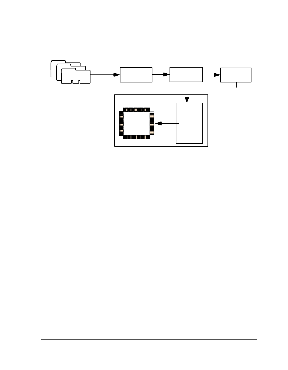
Program Development Flow
Figure 1-1 is a simplified view of the application development flow.
The development flow can be split into three phases:
1. “Compiling and Assembling”
2. “Linking”
3. “Loading, Splitting, or Both”
1-6 VisualDSP++ 4.5 Loader and Utilities Manual
Page 29
Introduction
SOURCE
FILES
.ASM, .C, .CP P
ASSEMBLER
AND/OR
COMPILER
PROCESSOR
.DOJ
TARG E T S YSTEM
BOOTING
UPON
RESET
LINKER
EXTERNAL
MEMORY
.DXE
.LDR
LOADER
AND/OR
SPLITTER
Figure 1-1. Program Development Flow
A brief description of each phase follows.
Compiling and Assembling
Input source files are compiled and assembled to yield object files. Source
files are text files containing C/C++ code, compiler directives, possibly a
mixture of assembly code and directives, and, typically, preprocessor commands. The assembler and compiler are documented in the VisualDSP++
4.5 Assembler and Preprocessor Manual and VisualDSP++ 4.5 C/C++ Compiler and Library Manual, which are part of the online help.
Linking
Under the direction of the linker description file (LDF) and linker settings, the linker consumes separately-assembled object and library files to
yield an executable file. If specified, the linker also produces the shared
memory files and overlay files. The linker output (.dxe files) conforms to
VisualDSP++ 4.5 Loader and Utilities Manual 1-7
Page 30

Program Development Flow
the ELF standard, an industry-standard format for executable files. The
linker also produces map files and other embedded information
(DWARF-2) used by the debugger.
These executable files are not readable by the processor hardware directly.
They are neither supposed to be burned onto an EPROM or flash memory
device. Executable files are intended for VisualDSP++ debugging targets,
such as the simulator or emulator. Refer to the VisualDSP++ 4.5 Linker
and Utilities Manual and online Help for information about linking and
debugging.
Loading, Splitting, or Both
Upon completing the debug cycle, the processor hardware needs to run on
its own, without any debugging tools connected. After power-up, the
processor’s on-chip and off-chip memories need to be initialized. The process of initializing memories is often referred to as booting. Therefore, the
linker output must be transformed to a format readable by the processor.
This process is handled by the loader and/or splitter utility. The
loader/splitter utility uses the debugged and tested executable files as well
as shared memory and overlay files as inputs to yield a processor-loadable
file.
VisualDSP++ 4.5 includes these loader and splitter utilities:
elfloader.exe (loader utility) for Blackfin, TigerSHARC, and
•
SHARC processors. The loader utility for Blackfin processors also
acts as a ROM splitter utility when evoked with the corresponding
switches.
• elfspl21k.exe (ROM splitter utility) for TigerSHARC and
SHARC processors.
The loader/splitter output is either a boot-loadable or non-bootable file.
The output is meant to be loaded onto the target. There are several ways
to use the output:
1-8 VisualDSP++ 4.5 Loader and Utilities Manual
Page 31

Introduction
• Download the loadable file into the processor’s PROM space on an
EZ-KIT Lite
VisualDSP++ Help for information on the Flash Programmer.
• Use VisualDSP++ to simulate booting in a simulator session (currently supported on ADSP-21060, ADSP-21061, ADSP-21065L,
ADSP-21160, and ADSP-21161 processors). Load the loader file
and then reset the processor to debug the booting routines. No
hardware is required: just point to the location of the loader file,
letting the simulator to do the rest. You can step through the boot
kernel code as it brings the rest of the code into memory.
• Store the loader file in an array for a multiprocessor system. A master (host) processor has the array in its memory, allowing a full
control to reset and load the file into the memory of a slave
processor.
®
board via the Flash Programmer plug-in. Refer to
Non-bootable Files Versus Boot-loadable Files
A non-bootable file executes from an external memory of the processor,
while a boot-loadable file is transported into and executes from an internal
memory of the processor. The boot-loadable file is then programmed into
an external memory device (burned into EPROM) within your target system. The loader utility outputs loadable files in formats readable by most
EPROM burners, such as Intel hex-32 and Motorola S formats. For
advanced usage, other file formats and boot modes are supported. (See
“File Formats” on page A-1.)
A non-bootable EPROM image file executes from an external memory of
the processor, bypassing the built-in boot mechanisms. Preparing a
non-bootable EPROM image is called splitting. In most cases (except for
Blackfin processors), developers working with floating- and fixed-point
processors use the splitter instead of the loader utility to produce a
non-bootable memory image file.
VisualDSP++ 4.5 Loader and Utilities Manual 1-9
Page 32

Program Development Flow
A booting sequence of the processor and application program design dictate the way loader/splitter utility is called to consume and transform
executable files:
• For Blackfin processors, loader and splitter operations are handled
by the loader utility program,
elfloader.exe. The splitter is
invoked by a different set of command-line switches than the
loader.
• For TigerSHARC and SHARC processors, splitter operations are
handled by the splitter program, elfspl21k.exe.
Loader Utility Operations
Common tasks performed by the loader utility can include:
• Processing the loader option settings or command-line switches.
• Formatting the output .ldr file according to user specifications.
Supported formats are binary, ASCII, hex-32, and more. Valid file
formats are described in “File Formats” on page A-1.
• Packing the code for a particular data format: 8-, 16- or 32-bit for
some processors.
• Adding the code and data from a specified initialization executable
file to the loader file, if applicable.
• Adding a boot kernel on top of the user code.
• If specified, preprogramming the location of the
.ldr file in a
specified PROM space.
• Specifying processor IDs for multiple input .dxe files for a
multiprocessor system, if applicable.
1-10 VisualDSP++ 4.5 Loader and Utilities Manual
Page 33

Introduction
You can run the loader utility from the VisualDSP++ Integrated Development and Development Environment (IDDE), when the IDDE is
available, or from the command line. In order to do so in the IDDE, open
the Project Options dialog box from the Project menu, and change the
project’s target type from Executable file to Loader File.
Loader utility operations depend on the loader options, which control
how the loader utility processes executable files into boot-loadable files,
letting you select features such as kernels, boot modes, and output file formats. These options are set on the Load pages of the Project Options
dialog box in the IDDE or on the loader command line. Option settings
on the Load pages correspond to switches typed on the
elfloader.exe
command line.
Splitter Utility Operations
Splitter utility operations depend on the splitter options, which control
how the splitter utility processes executable files into non-bootable files:
• For Blackfin processor, the loader utility includes the ROM splitter
capabilities invoked through the Project Options dialog box. Refer
to “Using ROM Splitter” on page 2-79. Option settings in the dialog box correspond to switches typed on the elfloader.exe
command line.
• For SHARC and TigerSHARC processors, change the project’s target type to Splitter file. The splitter options are set via the Project:
Split page of the Project Options dialog box. Refer to “Splitter for
SHARC and TigerSHARC Processors” on page 7-1. Option set-
tings in the dialog box correspond to switches typed on the
elfspl21k.exe command line.
VisualDSP++ 4.5 Loader and Utilities Manual 1-11
Page 34

Boot Modes
Boot Modes
Once an executable file is fully debugged, the loader utility is ready to
convert the executable file into a processor-loadable (boot-loadable) file.
The loadable file can be automatically downloaded (booted) to the processor after power-up or after a software reset. The way the loader utility
creates a boot-loadable file depends upon how the loadable file is booted
into the processor.
The boot mode of the processor is determined by sampling one or more of
the input flag pins. Booting sequences, highly processor-specific, are
detailed in the following chapters.
Analog Devices processors support different boot mechanisms. In general,
the following schemes can be used to provide program instructions to the
processors after reset.
• “No-Boot Mode”
• “PROM Boot Mode”
• “Host Boot Mode”
No-Boot Mode
After reset, the processor starts fetching and executing instructions from
EPROM/flash memory devices directly. This scheme does not require any
loader mechanism. It is up to the user program to initialize volatile
memories.
The splitter utility generates a file that can be burned into the PROM
memory.
1-12 VisualDSP++ 4.5 Loader and Utilities Manual
Page 35

Introduction
PROM Boot Mode
After reset, the processor starts reading data from a parallel or serial
PROM device. The PROM stores a formatted boot stream rather than raw
instruction code. Beside application data, the boot stream contains additional data, such as destination addresses and word counts. A small
program called a boot kernel (described on page 1-14) parses the boot
stream and initializes memories accordingly. The boot kernel runs on the
target processor. Depending on the architecture, the boot kernel may execute from on-chip boot RAM or may be preloaded from the PROM
device into on-chip SRAM and execute from there.
The loader utility generates the boot stream from the linker output (an
executable file) and stores it to file format that can be burned into the
PROM.
Host Boot Mode
In this scheme, the target processor is a slave to a host system. After reset,
the processor delays program execution until the slave gets signalled by the
host system that the boot process has completed. Depending on hardware
capabilities, there are two different methods of host booting. In the first
case, the host system has full control over all target memories. The host
halts the target while initializing all memories as required. In the second
case, the host communicates by a certain handshake with the boot kernel
running on the target processor. This kernel may execute from on-chip
ROM or may be preloaded by the host devices into the processor’s SRAM
by any bootstrapping scheme.
The loader/splitter utility generates a file that can be consumed by the
host device. It depends on the intelligence of the host device and on the
target architecture whether the host expects raw application data or a formatted boot stream.
VisualDSP++ 4.5 Loader and Utilities Manual 1-13
Page 36

Boot Kernels
In this context, a boot-loadable file differs from a non-bootable file in that
it stores instruction code in a formatted manner in order to be processed
by a boot kernel. A non-bootable file stores raw instruction code.
Boot Kernels
A boot kernel refers to the resident program in the boot ROM space
responsible for booting the processor. Alternatively (or in absence of the
boot ROM), the boot kernel can be preloaded from the boot source by a
bootstrapping scheme.
When a reset signal is sent to the processor, the processor starts booting
from a PROM, host device, or through a communication port. For example, an ADSP-2106x/2116x processor, brings a 256-word program into
internal memory for execution. This small program is a boot kernel.
The boot kernel then brings the rest of the application code into the processor’s memory. Finally, the boot kernel overwrites itself with the final
block of application code and jumps to the beginning of the application
program.
Some of the newer Blackfin processors (ADSP-BF531, ADSP-BF532,
ADSP-BF533, ADSP-BF534, ADSP-BF535, ADSP-BF536,
ADSP-BF537, ADSP-BF538, and ADSP-BF539) do not require to load a
boot kernel—a kernel is already present in the on-chip boot ROM. It
allows the entire application program’s body to be booted into the internal
and external memories of the processor. The boot kernel in the on-chip
ROM behaves similar to the second-stage loader of the ADSP-BF535 processors. The boot ROM has the capability to parse address and count
information for each bootable block.
1-14 VisualDSP++ 4.5 Loader and Utilities Manual
Page 37

Introduction
Boot Streams
The loader utility’s output (.ldr file) is essentially the same executable
code as in the input .dxe file; the loader utility simply repackages the executable as shown in Figure 1-2.
.DXE FILE
CODE
DATA
SYMBOLS
DEBUG
INFORMATION
A .DXE FILE INCLUDES:
- DSP INSTRUCTIONS (CODE AND DATA)
- SYMBOL TABLE AND SECTION INFORMATION
- TARGET PROCESSOR MEMORY LAYOUT
- DEBUG INFORMATION
.LDR FILE
CODE
DATA
SYMBOLS
DEBUG
INFORMATION
AN .LDR FILE INCLUDES:
- DSP INSTRUCTIONS (CODE AND DATA)
- RUDIMENTARYFORMATTING
(ALL DEBUG INFORMATION HAS
BEEN REMOVED)
Figure 1-2. A .dxe File Versus an .ldr File
Processor code and data in a loader file (also called a boot stream) is split
into blocks. Each code block is marked with a tag that contains information about the block, such as the number of words and destination in the
processor’s memory. Depending on the processor family, there can be
additional information in the tag. Common block types are “zero” (memory is filled with
0s); nonzero (code or data); and final (code or data).
Depending on the processor family, there can be other block types.
Refer to the following chapters to learn more about boot streams.
VisualDSP++ 4.5 Loader and Utilities Manual 1-15
Page 38

File Searches
File Searches
File searches are important in the loader utility operation. The loader utility supports relative and absolute directory names and default directories.
File searches occur as follows.
• Specified path—If relative or absolute path information is included
in a file name, the loader utility searches only in that location for
the file.
• Default directory—If path information is not included in the file
name, the loader utility searches for the file in the current working
directory.
• Overlay and shared memory files—The loader utility recognizes
overlay and shared memory files but does not expect these files on
the command line. Place the files in the directory that contains the
executable file that refers to them, or place them in the current
working directory. The loader utility can locate them when processing the executable file.
When providing an input or output file name as a loader/splitter command-line parameter, use these guidelines:
• Enclose long file names within straight quotes, “long file name”.
• Append the appropriate file extension to each file.
1-16 VisualDSP++ 4.5 Loader and Utilities Manual
Page 39

2 LOADER/SPLITTER FOR
BLACKFIN PROCESSORS
This chapter explains how the loader/splitter utility (elfloader.exe) is
used to convert executable (.dxe) files into boot-loadable or non-bootable
files for the ADSP-BF5xx Blackfin processors.
Refer to “Introduction” on page 1-1 for the loader utility overview.
Loader operations specific to Blackfin processors are detailed in the following sections.
• “Blackfin Processor Booting” on page 2-2
Provides general information on various boot modes, including
information on second-stage kernels:
• “ADSP-BF535 Processor Booting” on page 2-2
• “ADSP-BF531/BF532/BF533/BF534/BF536/BF537/
BF538/BF539 Processor Booting” on page 2-16
• “ADSP-BF561 and ADSP-BF566 Processor Booting” on
page 2-42
• “Blackfin Processor Loader Guide” on page 2-62
Provides reference information on the loader utility’s command-line syntax and switches.
VisualDSP++ 4.5 Loader and Utilities Manual 2-1
Page 40

Blackfin Processor Booting
Blackfin Processor Booting
A Blackfin processor can be booted from an 8- or 16-bit flash/PROM
memory or from an 8-,16-, or 24-bit addressable SPI memory. (The
ADSP-BF561/BF566 processors does not support 24-bit addressable SPI
memory boot.) There is also a no-boot option (bypass mode) in which
execution occurs from a 16-bit external memory.
At power-up, after a reset, the processor transitions into a boot mode
sequence configured by the BMODE pins (Table 2-1). The BMODE pins are
dedicated mode-control pins; that is, no other functions are performed by
these pins. The pins can be read through bits in the system reset configuration register SYSCR (Figure 2-2).
L
information on system configuration, peripherals, registers, and
operating modes.
ADSP-BF535 Processor Booting
Upon reset, an ADSP-BF535 processor jumps to an external 16-bit memory for execution (if BMODE = 000) or to the on-chip boot ROM (if
BMODE = 001, 010, or 011). Table 2-1 summarizes boot modes and code
execution start addresses for ADSP-BF535 processors.
Table 2-1. ADSP-BF535 Processor Boot Mode Selections
Boot Source BMODE[2:0] Execution Start Address
Refer to the processor’s datasheet and hardware reference for more
Execute from a 16-bit external memory (async
bank 0); no-boot mode (bypass on-chip boot
ROM); see on page 2-79.
Boot from an 8-bit/16-bit flash memory 001 0xF000 0000
Boot from an 8-bit address SPI0 serial EEPROM 010 0xF000 0000
000 0x2000 0000
1
1
2-2 VisualDSP++ 4.5 Loader and Utilities Manual
Page 41

Loader/Splitter for Blackfin Processors
Table 2-1. ADSP-BF535 Processor Boot Mode Selections (Cont’d)
Boot Source BMODE[2:0] Execution Start Address
Boot from a 16-bit address SPI0 serial EEPROM 011 0xF000 0000
Reserved 111—100 N/A
1 The processor jumps to this location after the booting is complete.
1
A description of each boot mode is as follows.
• “ADSP-BF535 Processor On-Chip Boot ROM” on page 2-4
• “ADSP-BF535 Processor Second-Stage Loader” on page 2-6
• “ADSP-BF535 and ADSP-BF531/BF532/BF533/BF534/
BF536/BF537/BF538/BF539 Processor No-Boot Mode” on
page 2-79
• “ADSP-BF535 Processor Boot Streams” on page 2-8
• “ADSP-BF535 Processor Memory Ranges” on page 2-14
VisualDSP++ 4.5 Loader and Utilities Manual 2-3
Page 42

Blackfin Processor Booting
ADSP-BF535 Processor On-Chip Boot ROM
The on-chip boot ROM for the ADSP-BF535 processor does the following (Figure 2-1).
Figure 2-1. ADSP-BF535 Processors: On-Chip Boot ROM
1. Sets up supervisor mode by exiting the
RESET interrupt service rou-
tine and jumping into the lowest priority interrupt (IVG15).
2. Checks whether the
RESET is a software reset and if so, whether to
skip the entire boot sequence and jump to the start of L2 memory
(
0xF000 0000) for execution. The on-chip boot ROM does this by
checking bit 4 of the system reset configuration register (
SYSCR). If
bit 4 is not set, the on-chip boot ROM performs the full boot
sequence. If bit 4 is set, the on-chip boot ROM bypasses the full
boot sequence and jumps to 0xF000 0000. The register settings are
shown in Figure 2-2.
2-4 VisualDSP++ 4.5 Loader and Utilities Manual
Page 43

Loader/Splitter for Blackfin Processors
System Reset Configuration Register (SYSCR)
X - state is initialized from mode pins during hardware reset
15 14 13 12 11 10 9 8 7 6 5 4 3 2 1 0
00000000 00 00XXX
0
Reset = dependent on pin values
No Boot on Software Reset
0 - Use BMODE to determine
boot source.
1 - Start executing from the
beginning of on-chip L2 memory
(or the beginning of ASYNC bank 0
when BMODE[2:0] = b#000).
BMODE 2-0 - RO
000 - Bypass boot ROM,
execute from 16-bit-wide
external memory.
001 - Use boot ROM to load
from 8-bit/16-bit flash.
010 - Use boot ROM to configure
and load boot code from
SPI0 serial ROM
(8-bit address range).
011 - Use boot ROM to configure
and load boot code from
SPI0 serial ROM
(16-bit address range).
100-111 - Reserved
Figure 2-2. ADSP-BF535 Processors: SYSCR Register
3. Finally, if bit 4 of the
SYSCR register is not set, performs the full
boot sequence. The full boot sequence includes:
D Checking the boot source (either flash/PROM or SPI mem-
ory) by reading BMODE2–0 from the SYSCR register.
D Reading the first four bytes from location 0x0 of the exter-
nal memory device. These four bytes contain the byte
count (
D Booting in N bytes into internal L2 memory starting at loca-
N), which specifies the number of bytes to boot in.
tion 0xF000 0000.
D Jumping to the start of L2 memory for execution.
The on-chip boot ROM boots in N bytes from the external memory. These
N bytes can define the size of the actual application code or a second-stage
loader that boots in the application code.
VisualDSP++ 4.5 Loader and Utilities Manual 2-5
Page 44
Blackfin Processor Booting
ADSP-BF535 Processor Second-Stage Loader
The only situation where a second-stage loader is unnecessary is when the
application code contains only one section starting at the beginning of L2
memory (
0xF000 0000).
A second-stage loader must be used in applications in which multiple segments reside in L2 memory or in L1 memory and/or SDRAM. In
addition, a second-stage loader must be used to change the wait states or
hold time cycles for a flash/PROM booting or to change the baud rate for
an SPI boot (see “Blackfin Loader Command-Line Switches” on
page 2-65 for more information on these features).
When a second-stage loader is used for booting, the following sequence
occurs.
1. Upon reset, the on-chip boot ROM downloads N bytes (the
second-stage loader) from external memory to address 0xF000 0000
in L2 memory (Figure 2-3).
Figure 2-3. ADSP-BF535 Processors: Booting With Second-Stage Loader
2-6 VisualDSP++ 4.5 Loader and Utilities Manual
Page 45

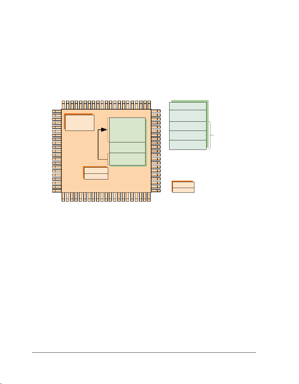
Loader/Splitter for Blackfin Processors
2. The second-stage loader copies itself to the bottom of L2 memory.
ADSP-BF535 Processor
0xEF00 0000
On-Chip
Boot ROM
L2 Memory
(0xF000 000 0)
2ndStage Loader
2ndStage Loader
or
Application
Code
2ndStage Loader
PROM/Flash o r SPI Device
4-Byte Header (N)
2ndStageLoader
Application
Code/Data
0x0
Figure 2-4. ADSP-BF535 Processors: Copying Second-Stage Loader
3. The second-stage loader downloads the application code and data
into the various memories of the Blackfin processor (Figure 2-5).
ADSP-BF535 Processor
0xEF00 0000
On-Chip
Boot ROM
L1 Memory
B
L2 Memory
(0xF000 0000)
2ndStage Loader
A
2ndStage Loader
or
Application
2ndStage Loader
Code
PROM/Flashor SPI Device
4-Byte Header (N)
2ndStage Loader
A
B
C
SDRAM
C
0x0
Application
Code/Data
Figure 2-5. ADSP-BF535 Processors: Booting Application Code
VisualDSP++ 4.5 Loader and Utilities Manual 2-7
Page 46
Blackfin Processor Booting
4. Finally, after booting, the second-stage loader jumps to the start of
L2 memory (
0xF000 0000) for application code execution
(Figure 2-6).
ADSP-BF535Processor
0xEF00 0000
On-Chip
Boot ROM
L1 Memory
B
L2 Memory
(0xF000 0000)
A
2ndStage Loader
PROM/Flash or SPI Device
4-Byte Header (N)
2nd Stage Loader
A
B
C
SDRAM
C
0x0
Application
Code/Data
Figure 2-6. ADSP-BF535 Processors: Starting Application Code
ADSP-BF535 Processor Boot Streams
The loader utility generates the boot stream and places the boot stream in
the output loader (.
ldr) file. The loader utility prepares the boot stream in
a way that enables the on-chip boot ROM and the second-stage loader to
load the application code and data to the processor memory correctly.
Therefore, the boot stream contains not only user application code but
also header and flag information that is used by the on-chip boot ROM
and the second-stage loader.
2-8 VisualDSP++ 4.5 Loader and Utilities Manual
Page 47

Loader/Splitter for Blackfin Processors
The following diagrams illustrate boot streams utilized by the
ADSP-BF535 processor’s boot kernel:
• “Loader Files Without a Second-Stage Loader” on page 2-9
• “Loader Files With a Second-Stage Loader” on page 2-10
• “Global Headers” on page 2-12
• “Blocks, Block Headers, and Flags” on page 2-13
Loader Files Without a Second-Stage Loader
Figure 2-7 is a graphical representation of an output loader file for 8-bit
PROM/flash boot and 8-/16-bit addressable SPI boot without the second-stage loader.
OUTPUT .LDR FILE
4-BYTE HEADER FOR
BYTE COUNT (N)
BYTE 0
BYTE 1
BYTE 2
BYTE 3
........
........
........
D7 D0
BYTE COUNT FOR
APPLICATION CODE
APPLICATION
CODE
(N W OR DS)
Figure 2-7. Loader File for 8-bit PROM/Flash & SPI Boot Without Second-Stage Loader
VisualDSP++ 4.5 Loader and Utilities Manual 2-9
Page 48

Blackfin Processor Booting
Figure 2-8 is a graphical representation of an output loader file for 16-bit
PROM/flash boot without the second-stage loader.
OUTPUT .LDR FILE
0x00
4-BYTE HEADER FOR
BYTE COUNT (N)
BYTE COUNT FOR
APPLICATION CODE
0x00
0x00
0x00
0x00
0x00
0x00
0x00
D15 D8 D7 D0
Figure 2-8. Loader
File for 16-bit PROM/Flash Boot Without Sec-
BYTE 0
BYTE 1
BYTE 2
BYTE 3
........
........
........
APPLICATION
CODE
(N WORDS)
ond-Stage Loader
Loader Files With a Second-Stage Loader
Figure 2-9 is a graphical representation of an output loader file for 8-bit
PROM/flash boot and 8- or 16-bit addressable SPI boot with the second-stage loader.
An output loader file for 16-bit PROM/flash boot with the second-stage
loader is illustrated in Figure 2-10.
2-10 VisualDSP++ 4.5 Loader and Utilities Manual
Page 49

OUTPUT.LDR FILE
OUTPUT.LDRF
ILE
4-BYTE HEADER FOR
BYTE COUNT (N)
BYTE 0
Loader/Splitter for Blackfin Processors
BYTE COUNTFOR
2ndSTAGE LOADER
BYTE 1
BYTE 2
........
BYTE 0
BYTE 1
BYTE 2
........
D7
Figure 2-9. Loader
Loader
0x00
0x00
0x00
0x00
0x00
2ndSTAGE
LOADER (NBYTES)
APPLICATION
CODE
(iN BLOCKS)
D0
File for 8-bit PROM/Flash/SPI Boot With Second-Stage
4-BYTE HEADER FOR
BYTE COUNT (N)
BYTE 0
BYTE 1
BYTE 2
........
SEE ALSO
FIGURE 2-12
SEE ALSO
FIGURE 2-14
BYTE COUNT FOR
2ndSTAGE LOADER
2ndSTAGE
LOADER
SEE ALSO
FIGURE2-12
BYTE 1
BYTE 3
BYTE 5
........
D15 D8
BYTE 0
BYTE 2
BYTE 4
........
D7 D0
APPLICATION
CODE
(iNBLOCKS)
SEE ALSO
FIGURE 2-14
Figure 2-10. Loader File for 16-bit PROM/Flash Boot With Second-Stage
Loader
VisualDSP++ 4.5 Loader and Utilities Manual 2-11
Page 50

Blackfin Processor Booting
Global Headers
Following the second-stage loader code and address in a loader file, there
is a 4-byte global header. The header provides the global settings for a
booting process (see Figure 2-11).
OUTPUT .LDR FILE
4 BYTES
BYTE COUNT (N)
BYTE COUNT F OR
2ndSTAGE LOADER
N BYTES
4 BYTES
4 BYTES
4 BYTES
N1 BYTES
2ndSTAGE LOADER
2ndSTAGE LOADER
ADDRESS
GLOBAL HEADER
SIZE O F APPLICATION
CODE (N1)
APPLICATION CODE
L2 MEMORY END ADDRESS
(FROM WHICH2ndSTAGE
LOADER RUNS)
SEE FIGURE 2-13
Figure 2-11. Global Header
A global header’s bit assignments for 8- and 16-bit PROM/flash boot are
in Figure 2-12.
015 14 13 12 11 10 9 8 76 5
Number of hold time cycles: 3 (default)
Number of wait states: 15 (default)
1 = 16-bit PROM/flash, 0 = 8-bit PROM/flash: 0 (default)
4
3 2 1
Figure 2-12. PROM/Flash Boot: Global Header Bit Assignments
2-12 VisualDSP++ 4.5 Loader and Utilities Manual
Page 51

Loader/Splitter for Blackfin Processors
A global header’s bit assignments for 8- and 16-bit addressable SPI booting are in Figure 2-13.
015 14 13 12 11 10 9 8 7 6 5
Baud rate: 0 = 500 kHz (default), 1 = 1 MHz, 2 = 2 MHz
321
4
Figure 2-13. SPI Boot: Global Header Bit Assignments
Blocks, Block Headers, and Flags
For application code, a block is the basic structure of the output
.ldr file
when the second-stage loader is used. All application code is grouped into
blocks. A block always has a header and a body if it is a non-zero block. A
block does not have a body if it is a zero block. A block structure is illustrated in Figure 2-14.
4 BYTES
N BYTES
4 BYTES
OUTPUT .LDR FILE
BYTE COUNT(N)
2ndSTAGE LOADER
2ndSTAGE LOADER
ADDRESS
SIZE OF APPLICATION
CODE (N1)
START ADDRESS
OF BLOCK 1
BYTE COUNT
OF BLOCK 1
FLAG FOR BLOCK 1
4 B YTES
4 BYT ES
2 BYT ES
BLOCK
HEADER
BLOCK
4 B YTES
4 B YTES
N1 BYTES
GLOBAL HEADER
SIZE OF APPLICATION
CODE (N1)
APPLICATION CODE
BODY OF BLOCK 1
START ADDRESS
OF BLOCK 2
BYTE COUNT
OF BLOCK 2
......
Figure 2-14. Application Block
VisualDSP++ 4.5 Loader and Utilities Manual 2-13
Page 52

Blackfin Processor Booting
A block header has three words: 4-byte clock start address, 4-byte block
byte count, and 2-byte flag word.
The ADSP-BF535 block flag word’s bits are illustrated in Figure 2-15.
015 14 13 12 11 10 9 8 7 6 5
Bit 15: 1 = Last Block, 0 = Not Last Block
321
4
Bit 0: 1 = Zero-Fill, 0 = No Zero-Fill
Figure 2-15. Block Flag Word Bit Assignments
ADSP-BF535 Processor Memory Ranges
Second-stage loaders are available for ADSP-BF535 processors in
VisualDSP++ 3.0 and higher. They allow booting to:
• L2 memory (
0xF000 0000)
• L1 memory
D Data bank A SRAM (0xFF80 0000)
D Data bank B SRAM (0xFF90 0000)
D Instruction SRAM (0xFFA0 0000)
D Scratchpad SRAM (0xFFB0 0000)
•SDRAM
D Bank 0 (0x0000 0000)
D Bank 1 (0x0800 0000)
D Bank 2 (0x1000 0000)
D Bank 3 (0x1800 0000)
SDRAM must be initialized by user code before any instructions or
L
data are loaded into it.
2-14 VisualDSP++ 4.5 Loader and Utilities Manual
Page 53

Loader/Splitter for Blackfin Processors
Second-Stage Loader Restrictions
Using the second-stage loader imposes the following restrictions.
• The bottom of L2 memory must be reserved during booting. These
locations can be reallocated during runtime. The following locations pertain to the current second-stage loaders.
D For 8- and 16-bit PROM/flash booting, reserve
0xF003 FE00—0xF003 FFFF (last 512 bytes).
D For 8- and 16-bit addressable SPI booting, reserve
0xF003 FD00—0xF003 FFFF (last 768 bytes).
• If segments reside in SDRAM memory, configure the SDRAM registers accordingly in the second-stage loader before booting.
D Modify a section of code called “SDRAM setup” in the
second-stage loader and rebuild the second-stage loader.
• Any segments residing in L1 instruction memory
(0xFFA0 0000–0xFFA0 3FFF) must be 8-byte aligned.
D Declare segments, within the .ldf file, that reside in L1
instruction memory at starting locations that are 8-byte
aligned (for example, 0xFFA0 0000, 0xFFA0 0008,
0xFFA0 0010, and so on).
D Use the .ALIGN 8; directives in the application code.
The two reasons for these restrictions are:
L
• Core writes into L1 instruction memory are not allowed.
• DMA from an 8-bit external memory is not possible since
the minimum width of the external bus interface unit
(EBIU) is 16 bits.
VisualDSP++ 4.5 Loader and Utilities Manual 2-15
Page 54

Blackfin Processor Booting
Load bytes into L1 instruction memory by using the instruction test command and data registers, as described in the Memory chapter of the
appropriate hardware reference manual. These registers transfer 8-byte
sections of data from external memory to internal L1 instruction memory.
ADSP-BF531/BF532/BF533/BF534/BF536/BF537/ BF538/BF539 Processor Booting
Upon reset, an ADSP-BF531/BF532/BF533/BF534/BF536/BF537/
BF538/BF539 processor jumps to the on-chip boot ROM or jumps to
16-bit external memory for execution (if BMODE = 0) located at
0xEF00 0000. Table 2-2 shows boot modes and execution start addresses
for ADSP-BF531, ADSP-BF532, ADSP-BF533, ADSP-BF538, and
ADSP-BF539 processors.
Table 2-3 shows boot modes for ADSP-BF534/BF536/BF537 processors,
which in addition to all ADSP-BF531/BF532/BF533 processor boot
modes, also can boot from a TWI serial device, a TWI host, and a UART
host.
2-16 VisualDSP++ 4.5 Loader and Utilities Manual
Page 55

Loader/Splitter for Blackfin Processors
Table 2-2. Processor Boot Mode Selections for ADSP-BF531/BF532/
BF533/BF538/BF539 Processors
Execution Start Address
Boot Source BMODE[1:0]
ADSP-BF531
ADSP-BF532
ADSP-BF538
ADSP-BF533
ADSP-BF539
Execute from 16-bit External ASYNC bank 0
memory (no-boot mode or bypass on-chip
boot ROM); see on page 2-79
Boot from 8- or 16-bit PROM/flash 01 0xFFA0 8000 0xFFA0 0000
Boot from an SPI host in SPI slave mode 10 0xFFA0 8000 0xFFA0 0000
Boot from an 8-, 16-, or 24-bit addressable
SPI memory in SPI master boot mode with
support for Atmel AT45DB041B,
AT45DB081B, and AT45DB161B DataFlash
devices
00 0x2000 0000 0x2000 0000
11 0xFFA0 8000 0xFFA0 0000
Table 2-3. ADSP-BF534/BF536/BF537 Processor Boot Modes
Boot Source BMODE[2:0]
Executes from external 16-bit memory connected to ASYNC
bank 0; (no-boot mode or bypass on-chip boot ROM); see
on page 2-79
Boots from 8/16-bit PROM/flash 001
Reserved 010
Boots from an 8-, 16-, or 24-bit addressable SPI memory in
SPI master mode with support for Atmel AT45DB041B,
AT45DB081B, and AT45DB161B DataFlash devices
000
011
Boots from an SPI host in SPI slave mode 100
Boots from a TWI serial device 101
Boots from a TWI host 110
Boots from a UART host 111
VisualDSP++ 4.5 Loader and Utilities Manual 2-17
Page 56

Blackfin Processor Booting
A description of each boot mode is as follows.
• “ADSP-BF531/BF532/BF533/BF534/BF536/BF537/BF538/
BF539 Processor On-Chip Boot ROM” on page 2-19
• “ADSP-BF531/BF532/BF533/BF534/BF536/BF537/BF538/
BF539 Processor in SPI Slave Boot Mode” on page 2-21
• “ADSP-BF531/BF532/BF533/BF534/BF536/BF537/BF538/
BF539Processor in SPI Master Boot Mode” on page 2-23
• “ADSP-BF534/BF536/BF537 TWI Master Boot Mode (BMODE
= 101)” on page 2-27
• “ADSP-BF534/BF536/BF537 TWI Slave Boot Mode (BMODE =
110)” on page 2-29
• “ADSP-BF534/BF536/BF537 UART Slave Mode Boot via Master
Host (BMODE = 111)” on page 2-30
• “ADSP-BF535 and ADSP-BF531/BF532/BF533/BF534/
BF536/BF537/BF538/BF539 Processor No-Boot Mode” on
page 2-79
2-18 VisualDSP++ 4.5 Loader and Utilities Manual
Page 57

Loader/Splitter for Blackfin Processors
ADSP-BF531/BF532/BF533/BF534/BF536/BF537/BF538/ BF539 Processor On-Chip Boot ROM
The on-chip boot ROM for ADSP-BF531/BF532/BF533/BF534/
BF536/BF537/BF538/BF539 processors does the following.
1. Sets up supervisor mode by exiting the
RESET interrupt service
routine and jumping into the lowest priority interrupt (IVG15).
Note that the on-chip boot ROM of the ADSP-BF534/BF536 and
ADSP-BF537 processors executes at the Reset priority level, does
not degrade to the lowest priority interrupt.
2. Checks whether the RESET was a software reset and, if so, whether
to skip the entire sequence and jump to the start of L1 memory
(0xFFA0 0000 for ADSP-BF533/BF534/BF536/BF537/BF539
processors; 0xFFA0 8000 for ADSP-BF531/BF532/BF538) for
execution. The on-chip boot ROM does this by checking the
NOBOOT bit (bit 4) of the system reset configuration register (SYSCR).
See Figure 2-16. If bit 4 is not set, the on-chip boot ROM performs the full boot sequence. If bit 4 is set, the on-chip boot ROM
bypasses the full boot sequence and jumps to the start of L1
memory.
X - state is initialized from mode pins during hardware re set
0xFFC0 0104
15 14 13 12 11 10 9 8 7 6 5 4 3 2 1 0
0 000000 0 XX
X0000 0
Reset = dependent on pin
values
NOBOOT (No Boot on Software Reset)
0 - Use BMODE to determine
boot source
1 - Start executing from the
the EVT1 vector.
EVT1 defaults to 0xFFA00000,
except the ADSP-BF531/BF532
and ADSP-BF538 processors,
where it defaults to 0xFFA08000.
BMODE[2:0] (Boot Mode) - RO
The BMODE bit field represents
the BMODE pin settings. Various
processors populate two, three or
four bits according to the number
of featured BMODE pins (see
Table 2-2 and Table 2-3.
Figure 2-16. System Reset Configuration Register
VisualDSP++ 4.5 Loader and Utilities Manual 2-19
Page 58

Blackfin Processor Booting
3. The
NOBOOT bit, if bit 4 of the SYSCR register is not set, performs the
full boot sequence (Figure 2-17).
ADSP-BF531/BF532/BF533 Processor
L1 Memory
0xEF00 0000
On-Chip
Boot RO M
Block 1
Block 3
........
PROM/Flash or SPI Device
10-Byte Header for Block 1
Block 1
10-Byte Header for Block 2
Block 2
10-Byte Header for Block 3
Block 3
........
10-Byte Header for Block n
Block n
SDRAM
Block 2
App.
Code/
Data
Figure 2-17. ADSP-BF531/BF532/BF533/BF534/BF536/BF537/BF538/
BF539 Processors: Booting Sequence
The booting sequence for ADSP-BF531/BF532/BF533/BF534/BF536/
BF537/BF538/BF539 processors is different from that for ADSP-BF535
processors. The on-chip boot ROM for the former processors behaves
similar to the second-stage loader of ADSP-BF535processors. The boot
ROM has the capability to parse address and count information for each
bootable block. This alleviates the need for a second-stage loader because a
full application can be booted to the various memories with just the
on-chip boot ROM.
2-20 VisualDSP++ 4.5 Loader and Utilities Manual
Page 59

Loader/Splitter for Blackfin Processors
The loader utility converts the application code (
file by parsing the code and creating a file that consists of different blocks.
Each block is encapsulated within a 10-byte header, which is illustrated in
Figure 2-17 and detailed in the following section. The headers, in turn,
are read and parsed by the on-chip boot ROM during booting.
The 10-byte header provides all information the on-chip boot ROM
requires—where to boot the block to, how many bytes to boot in, and
what to do with the block.
ADSP-BF531/BF532/BF533/BF534/BF536/BF537/BF538/ BF539 Processor in SPI Slave Boot Mode
For SPI slave mode booting, the ADSP-BF531/BF532/BF533/
BF536/BF537/BF538/BF539
device, and a host device is used to boot the processor.
L
Figure 2-18 shows the pin-to-pin connections needed for SPI slave mode.
The host does not need any knowledge of the loader file stream to boot
the Blackfin processor. It must be configured to send one byte at a time
from the loader file in ASCII format. In the above setup, a PFx signal is the
feedback strobe from the Blackfin processor to the master host device.
This is the signal used by the Blackfin processor to hold off the host during certain times within the boot process (specifically during init code
execution and zero-fill blocks). When
host device must discontinue sending bytes to the Blackfin processor.
When
bytes from where it left off. Since the
until the first block has been processed, consider using a resistor to pull
down the feedback strobe.
This boot mode is not supported in ADSP-BF531/BF532/BF533/
silicon revision 0.2 and earlier.
PFx is de-asserted (low), the master host device resumes sending
processor is configured as an SPI slave
PFx is asserted (high), the master
PFx pin is not driven by the slave
.dxe) into the loadable
BF534/
VisualDSP++ 4.5 Loader and Utilities Manual 2-21
Page 60

Blackfin Processor Booting
Host
(Master SPI
Device)
ADSP-BF533
(Slave SPI)
Device)
SPICLK
S_SEL
MOSI
MISO
FLAG /
Interrupt
SPICLK
SPISS
MOSI
MISO
PFx
Figure 2-18. Pin-to-Pin Connections for
ADSP-BF531/BF532/BF533/
BF534/ BF536/BF537/BF538/BF539
Pro-
cessor SPI Slave Mode
For the ADSP-BF534/BF5356/BF537processors, a pull down or pull up
may be used. The on-chip boot ROM senses the polarity of this signal and
asserts it by driving it to the opposite state of the external pull up/down.
This
PFx number is going to be user-defined and is embedded within the
loader file. The loader utility embeds the number in bits [8:5] of the FLAG
field within every 10-byte header. The loader utility does this by using the
“-pFlag #” command-line switch where number is the intended PF flag
used by the Blackfin slave and has a value between
1 and 15.
L
bits [8:5] of the
feedback signal to the host. Since
/SPISS pin, which is mandatory for successful SPI slave boot,
FLAG is 0, indicating that PF0 is assumed as the
PF0 is multiplexed with the
always use the “-pFlag #” switch and specify a value other than
0.
2-22 VisualDSP++ 4.5 Loader and Utilities Manual
If the “-pFlag #” switch is not used, the default value placed within
Page 61

Loader/Splitter for Blackfin Processors
ADSP-BF531/BF532/BF533/BF534/BF536/BF537/BF538/ BF539Processor in SPI Master Boot Mode
For SPI master mode booting, the ADSP-BF531/BF532/BF533/
BF536/BF537/BF538/BF539
processor is configured as a SPI master con-
BF534
/
nected to a SPI memory. The following shows the pin-to-pin connections
needed for this mode.
Figure 2-19 shows the pin-to-pin connections needed for SPI master
mode.
A pull-up resistor on MISO is required for this boot mode to work
L
properly. For this reason, the ADSP-BF531/BF532/BF533/
BF536/BF537/BF538/ BF539
processor reads a 0xFF on the MISO
BF534
pin if the SPI memory is not responding (that is, no data written
on the MISO pin by the SPI memory).
ADSP-BF533
(Master SPI
Device)
SPICLK
PF2
V
DDEXT
10KΩ
SPI Memory
(Slave SPI
Device)
SPICLK
CS
/
MOSI
MISO
MOSI
MISO
Figure 2-19. Pin-to-pin connections for ADSP-BF531/BF532/BF533 Processor SPI Master Mode
VisualDSP++ 4.5 Loader and Utilities Manual 2-23
Page 62

Blackfin Processor Booting
Although the pull-up resistor on the
pull-up resistors might also be worthwhile as well. Pull up the PF2 signal
to ensure the SPI memory is not activated while the Blackfin processor is
in reset.
L
The SPI memories supported by this interface are standard 8/16/24-bit
addressable SPI memories (the read sequence is explained below) and the
following Atmel SPI DataFlash devices: AT45DB041B, AT45DB081B,
AT45DB161B. The ADSP-BF534/BF536/BF537 processors additionally
support the AT45DB321, AT45DB642, and AT45DB1282 devices.
Standard 8/16/24-bit addressable SPI memories take in a read command
byte of 0x03, followed by one address byte (for 8-bit addressable SPI
memories), two address bytes (for 16-bit addressable SPI memories), or
three address bytes (for 24-bit addressable SPI memories). After the correct read command and address are sent, the data stored in the memory at
the selected address is shifted out on the
tially from that address with continuing clock pulses. Analog Devices has
tested the following standard SPI memory devices.
On ADSP-BF531/BF532/BF533 of silicon revision 0.2 and earlier,
the CPHA and CPOL bits within the SPI control (SPICTL) register
were both set to 1. (Refer to the ADSP-BF533 Blackfin Processor
Hardware Reference for information on these bits.) For this reason,
the SPI memory may detect an erroneous rising edge on the clock
signal when it recovers from three-state. If the boot process fails
because of this situation, a pull-up resistor on the SPICLK signal
alleviates the problem. On silicon revision 0.3, this was fixed by
setting CPHA = CPOL = 0 within the SPI control register.
MISO line is mandatory, additional
MISO pin. Data is sent out sequen-
• 8-bit addressable SPI memory: 25LC040 from Microchip
• 16-bit addressable SPI memory: 25LC640 from Microchip
• 24-bit addressable SPI memory: M25P80 from STMicroelectronics
2-24 VisualDSP++ 4.5 Loader and Utilities Manual
Page 63

Loader/Splitter for Blackfin Processors
SPI Memory Detection Routine
Since
BMODE = 11 supports booting from various SPI memories, the
on-chip boot ROM detects what type of memory is connected. To determine the type of memory connected to the processor (8-, 16-, or 24-bit
addressable), the on-chip boot ROM sends the following sequence of
bytes to the SPI memory until the memory responds back. The SPI memory does not respond back until it is properly addressed. The on-chip boot
ROM does the following.
1. Sends the read command, 0x03, on the MOS1 pin, then does a
dummy read of the MISO pin.
2. Sends an address byte, 0x00, on the MOSI pin, then does a dummy
read of the MISO pin.
3. Sends another byte, 0x00, on the MOSI pin and checks whether the
incoming byte on the MISO pin is anything other than 0xFF (this is
the value from the pull-up resistor. For more information, refer to
the following note.) An incoming byte that is not 0xFF means that
the SPI memory has responded back after one address byte, and an
8-bit addressable SPI memory device is assumed to be connected.
4. If the incoming byte is 0xFF, the on-chip boot ROM sends another
byte, 0x00, on the MOSI pin and checks whether the incoming byte
on the
MISO pin is anything other than 0xFF. An incoming byte
other than 0xFF means that the SPI memory has responded back
after two address bytes, and a 16-bit addressable SPI memory
device is assumed to be connected.
5. If the incoming byte is 0xFF, the on-chip boot ROM sends another
byte, 0x00, on the MOSI pin and checks whether the incoming byte
on the
other than
MISO pin is anything other than 0xFF. An incoming byte
0xFF means that the SPI memory has responded back
after three address bytes, and a 24-bit addressable SPI memory
device is assumed to be connected.
VisualDSP++ 4.5 Loader and Utilities Manual 2-25
Page 64

Blackfin Processor Booting
6. If an incoming byte is
back), the on-chip boot ROM assumes that one of the following
Atmel DataFlash devices are connected: AT45DB041B,
AT45DB081B, or AT45DB161B. These DataFlash devices have a
different read sequence than the one described above for standard
SPI memories. The on-chip boot ROM determines which of the
above Atmel DataFlash memories are connected by reading the status register.
L
L
For the SPI memory detection routine explained above, the
on-chip boot ROM on ADSP-BF531/BF532/BF533 silicon revision 0.2 and earlier checks whether the incoming data on the MISO
pin is 0x00 (first byte of the loader file). The on-chip boot ROM in
silicon revision 0.3 checks whether the incoming data on the MISO
pin is anything other than 0xFF. For this reason, SPI loader files
built for silicon revision 0.2 and earlier must have the first byte as
0x00. For silicon revision 0.3, the first byte of the loader file is set
to 0x40.
While traditional Atmel DataFlash memories ignore the standard
0x03 SPI read command, newer revisions simulate standard 24-bit
addressable SPI memories and return data earlier than one may
expect. Consequently, newer DataFlash revisions need to be programmed in power-of-2 page size mode. Former revisions are
required to be in traditional page size mode.
0xFF (meaning no devices have responded
The SPI baud rate register is set to
system clock, results in a 54 MHz / (2 * 133) = 203 kHz baud rate. On
the ADSP-BF533 EZ-KIT Lite board, the default system clock frequency
is 54 MHz.
2-26 VisualDSP++ 4.5 Loader and Utilities Manual
133, which, when based on a 54 MHz
Page 65

Loader/Splitter for Blackfin Processors
ADSP-BF534/BF536/BF537 TWI Master Boot Mode (BMODE = 101)
The Blackfin processor selects the slave EEPROM with the unique ID
0xA0, and submits successive read commands to the device starting at two
byte internal address 0x0000 and begins clocking data into the processor.
The serial EEPROM must be two-byte addressable. The EEPROM’s
device select bits A2–0 must be 0s (tied low). The I2C EPROM device
should comply with Philips I2C Bus Specification version 2.1 and should
have the capability to auto increment its internal address counter such that
the contents of the memory device can be read sequentially (see
Figure 2-20).
The TWI controller is programmed so as to generate a 30% duty cycle
clock in accordance with the I2C clock specification for fast-mode
operation.
L
Figure 2-20. TWI Master Boot Mode
In both TWI master and slave boot modes, the upper 256 bytes
starting at address 0xFF90 3F00 must not be used. The boot ROM
code uses this space for the TWI boot modes to temporarily hold
the serial data which is then transferred to L1 instruction memory
using DMA.
VisualDSP++ 4.5 Loader and Utilities Manual 2-27
Page 66

Blackfin Processor Booting
In Figure 2-21, The TWI controller outputs on the bus the address of the
2
I
C device to boot from: 0xA0 where the least significant bit indicates the
direction of the transfer. In this case, it is a write (0) in order to write the
first 2 bytes of the internal address from which to start booting (0x00).
Figure 2-21. TWI Master Booting
Figure 2-22 shows the TWI init and zero-fill blocks.
Figure 2-22. TWI Init and Zero-Fill Blocks
2-28 VisualDSP++ 4.5 Loader and Utilities Manual
Page 67

Loader/Splitter for Blackfin Processors
ADSP-BF534/BF536/BF537 TWI Slave Boot Mode (BMODE = 110)
2
The I
C host agent selects the slave (Blackfin processor) with the 7-bit
slave address of 0x5F. The processor replies with an acknowledgement and
the host can then download the boot stream. The I2C host agent should
comply with Philips I2C Bus Specification version 2.1. The host device sup-
plies the serial clock (see Figure 2-23 and Figure 2-24).
Figure 2-23. TWI Slave Booting
Figure 2-24. TWI Slave Boot Mode
VisualDSP++ 4.5 Loader and Utilities Manual 2-29
Page 68

Blackfin Processor Booting
L
ADSP-BF534/BF536/BF537 UART Slave Mode Boot via Master Host (BMODE = 111)
UART booting on the Blackfin processor is supported only through
UART0, and the Blackfin processor is always a slave.
Using an autobaud detection sequence, a boot-stream-formatted program
is downloaded by the host. The host agent selects a bit rate within the
UART’s clocking capabilities. When performing the autobaud, the UART
expects an “@” character (0x40, eight bits data, one start bit, one stop bit,
no parity bit) on the UART0 RXD input to determine the bit rate. The
hardware support and the mathematical operations to perform for this
autobaud detection is explained in Chapter 15, “General-Purpose Timers”
of the ADSP-BF537 Blackfin Processor Hardware Reference. The boot kernel then replies with an acknowledgement, and then the host can
download the boot stream. The acknowledgement consists of the following four bytes: 0xBF, UART0_DLL, UART0_DLH, 0x00. The host is requested
not to send further bytes until it has received the complete acknowledge
string. Once the
stream at once. The host must know the total byte count of the boot
stream, but the host does not require any knowledge about the content of
the boot stream.
On the Blackfin processor, in both TWI master and slave boot
modes, the upper 256 bytes of data bank A starting at address
0xFF90 3F00 must not be used. The boot ROM code uses this
space for the TWI boot modes to temporarily hold the serial data
which is then transferred to L1 instruction memory using DMA.
0x00 byte is received, the host can send the entire boot
When the boot kernel is processing ZEROFILL or INIT blocks, it may
require extra processing time and needs to hold the host off from sending
more data. This is signalled with the
any GPIO of port
FLAG word of all block headers. The boot kernel is not permitted to drive
any of the GPIOs before the first block header has been received and eval-
2-30 VisualDSP++ 4.5 Loader and Utilities Manual
G. The GPIO, which is actually used, is encoded in the
HWAIT output which can operate on
Page 69

Loader/Splitter for Blackfin Processors
uated completely. Therefore, a pulling resistor on the
HWAIT signal is
recommended. If the resistor pulls down to ground, the host is always permitted to send when the HWAIT signal is low and must pause transmission
when HWAIT is high. The Blackfin UART module does not provide
extremely large receive FIFOs, so the host is requested to test HWAIT at
every transmitted byte.
As indicated in Figure 2-25, the HWAIT feedback may connect to the
clear-to-send (CTS) input of an EIA-232E compatible host device, resulting in a subset of a so-called hardware handshake protocol. The host is
requested to interrogate the HWAIT signal before every individual byte. At
boot time the Blackfin processor does not evaluate any request-to-send
(RTS) signal driven by the host.
Figure 2-25. UART Slave Boot Mode
VisualDSP++ 4.5 Loader and Utilities Manual 2-31
Page 70
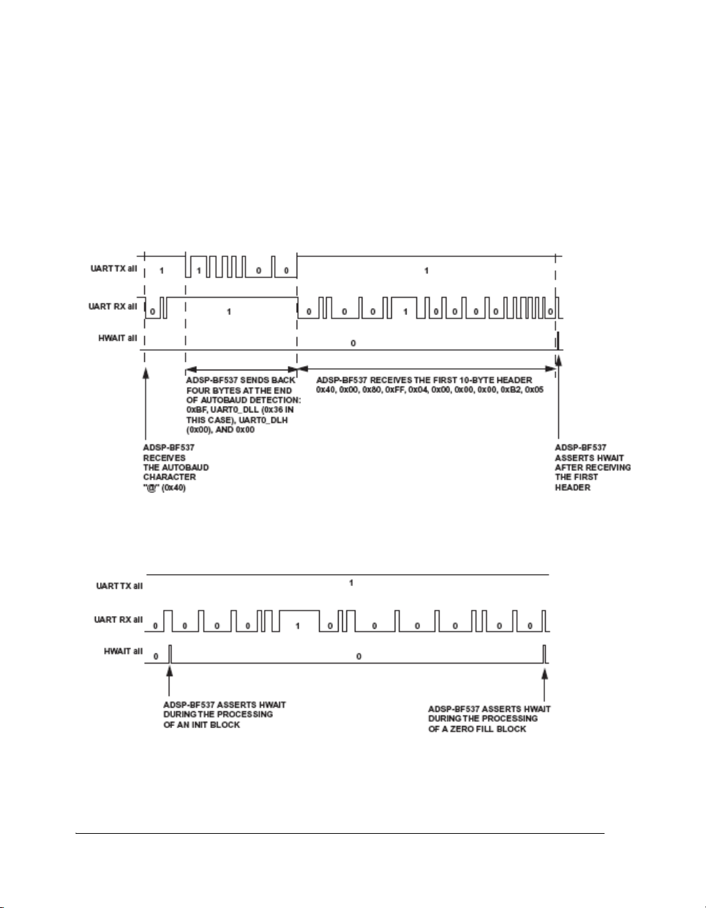
Blackfin Processor Booting
Figure 2-25 shows the logical interconnection between the UART host
and the Blackfin device as required for booting. The figure does not show
physical line drivers and level shifters that are typically required to meet
the individual UART-compatible standards. Figure 2-26 and Figure 2-27
provide more information about UART booting.
Figure 2-26. UART Slave Booting
Figure 2-27. UART Init and Zero Fill Blocks
2-32 VisualDSP++ 4.5 Loader and Utilities Manual
Page 71

Loader/Splitter for Blackfin Processors
ADSP-BF531/BF532/BF533/BF534/BF536/BF537/BF538/ BF539 Processor Boot Streams
The following sections describe the boot stream, header, and flag framework for the ADSP-BF531, ADSP-BF532, ADSP-BF533, ADSP-BF534,
ADSP-BF536, ADSP-BF537, ADSP-BF538, and ADSP-BF539
processors.
• “ADSP-BF531/BF532/BF533/BF534/BF536/BF537/BF538/
BF539 Blocks, Block Headers, and Flags” on page 2-33
• “Initialization Blocks” on page 2-36
The ADSP-BF531/BF532/BF533/BF534/BF536/BF537/BF538/BF539
processor boot stream is similar to the boot stream that uses a second-stage
kernel of ADSP-BF535 processors (detailed in “Loader Files With a Sec-
ond-Stage Loader” on page 2-10). However, since the former processors
do not employ a second-stage loader, their boot streams do not include
the second-stage loader code and the associated 4-byte header on the top
of the kernel code. There is also no 4-byte global header.
ADSP-BF531/BF532/BF533/BF534/BF536/BF537/BF538/ BF539 Blocks, Block Headers, and Flags
As the loader utility converts the code from an input
.dxe file into blocks
comprising the output loader file, each block receives a 10-byte header
(Figure 2-28), followed by a block body (if it is a non-zero block) or
no-block body (if it is a zero block). A description of the header structure
can be found in Table 2-4.
Table 2-4. ADSP-BF531/BF532/BF533 Block Header Structure
Bit Field Description
Address 4-byte address at which the block resides in memory.
Count 4-byte number of bytes to boot.
VisualDSP++ 4.5 Loader and Utilities Manual 2-33
Page 72

Blackfin Processor Booting
Table 2-4. ADSP-BF531/BF532/BF533 Block Header Structure (Cont’d)
Bit Field Description
Flag 2-byte flag containing information about the block; the following text
describes the flag structure.
BLOCK
HEADER OF .DXE 1 COUNT
10-BYTE HEADER
4-BYTE ADDRESS
4-BYTE COUNT
2-BYTE FLAG
BOOT STREAM OF THE
1stEXECUTABLE (.DXE 1)
.DXE 1 BYTE COUNT
BLOCK 1 HEADER
BLOCK 2 BODY
BLOCK 2 HEADER
BLOCK 2 BODY
......
......
HEADER OF .DXE 2 COUNT
BOOT STREAM OF THE
2ndEXECUTABLE (.DXE 2)
Figure 2-28.
ADSP-BF531/BF532/BF533/BF534/BF536/BF537/BF538
.DXE 2 BYTE COUNT
......
......
BF539 Processors: Boot Stream Structur
SEE FLAG INFORMATION
/
e
2-34 VisualDSP++ 4.5 Loader and Utilities Manual
Page 73

Loader/Splitter for Blackfin Processors
Refer to Figure 2-29 and Table 2-5 for the flag’s bit descriptions.
Table 2-5. Flag Structure
Bit Field Description
Zero-fill block Indicates that the block is for a buffer filled with zeros. The body of a zero
block is not included within the loader file. When the loader utility parses
through the .dxe file and encounters a large buffer with zeros, it creates a
zero-fill block to reduce
no block body in the block.
Ignore block Indicates that the block is not to be booted into memory; skips the block and
moves on to the next one. Currently is not implemented for application code.
.ldr file size and boot time. If this bit is set, there is
Initialization
block
Processor type Indicates the processor, either ADSP-BF531/BF532/BF538 or
Last block Indicates that the block is the last block to be booted into memory. After the
Compressed
block
Indicates that the block is to be executed before booting. The initialization
block indicator allows the on-chip boot ROM to execute a number of instructions before booting the actual application code. When the on-chip boot ROM
detects an init block, it boots the block into internal memory and makes a
CALL to it (initialization code must have an RTS at the end).
This option allows the user to run initialization code (such as SDRAM initialization) before the full boot sequence proceeds. Figure 2-30 and Figure 2-31
illustrate the process. Initialization code can be included within the
by using the -init switch (see “-init filename.dxe” on page 2-67).
See “Initialization Blocks” on page 2-36 for more information.
ADSP-BF533/BF534/BF536/BF537/BF539. After booting is complete, the
on-chip boot ROM jumps to
ADSP-BF533/BF536/BF537/BF539 processor and to 0xFFA0 8000 for the
ADSP-BF531/BF532/BF538 processor.
last block, the processor jumps to the start of L1 memory for application code
execution. When it jumps to L1 memory for code execution, the processor is
still in supervisor mode and in the lowest priority interrupt (
Indicates that the block contains compressed data. The compressed block can
include a number of blocks compressed together to form a single compressed
block.
0xFFA0 0000 for the
.ldr file
IVG15).
Note that the ADSP-BF534/BF536/BF537 processor can have a special
last block if the boot mode is two-wire interface (TWI). The loader utility
saves all the data from 0xFF903F00 to 0xFF903FFF and makes the last block
VisualDSP++ 4.5 Loader and Utilities Manual 2-35
Page 74

Blackfin Processor Booting
015 14 13 12 11 10 9 8 7 6 5
Last Block:
1 = Last Block
0 = Not Last Block
Compressed Block:
1 = Compressed Block
0 = Not Compressed Block
Port Number:
00 = Disabled, 01 =Port F
10 = Port G, 11 = Port H
Programmable Flag:
0 = Default, Selectable from 0–15
Ignore Block: 1 = Ignore Block, 0 = Do Not Ignore Block
Initialization Block: 1 = Init Block, 0 = No Init Block
Processor Type: 1 = ADSP-BF533/534/536/537/538/539
0 = ADSP-BF531/BF532
Zero-Fill: 1 = Zero-Fill Block, 0 = No Zero-Fill Block
Bits 14, 12–11 are reserved for future use
321
4
Figure 2-29. Flag Bit Assignments for 2-Byte Block Flag Word
with the data. The loader utility, however, creates a regular last block if no
data is in that memory range. The space of
0xFF903F00 to 0xFF903FFF is
saved for the boot ROM to use as a data buffer during a boot process.
Initialization Blocks
-init filename option directs the loader utility to produce the ini-
The
tialization blocks from the initialization section’s code in the named file.
The initialization blocks are placed at the top of a loader file. They are
executed before the rest of the code in the loader file booted into the
memory (see Figure 2-30).
Following execution of the initialization blocks, the boot process
continues with the rest of data blocks until it encounters a final block (see
Figure 2-31). The initialization code example follows in Listing 2-1 on
page 2-38.
2-36 VisualDSP++ 4.5 Loader and Utilities Manual
Page 75

Loader/Splitter for Blackfin Processors
ADSP-BF531/BF532/BF533 PROCESSOR
L1 Memory
0xEF00 0000
On-Chip
Boot ROM
Init Blocks
PROM/FLASHOR SPI
SDRAM BLOCK HEADER
BLOCK N 10-BYTE HEA DER
Figure 2-30. ADSP-BF531/BF532/BF533/
BF539
Processors: Initialization Block Execution
ADSP-BF531/BF532/BF533 PROCESSOR
L1 Memory
0xEF00 0000
On-Ch p
Boot ROM
i
Init Block
L1 Block
A
DEVICE
INIT BLOCK HEADER
INIT BLOCKS
L1 BLOCK HEADER
L1 BLOCK
APP.
SDRAM BLOCK
........
BLOCK N
CODE/
DATA
SDRAM
BF534/BF536/BF537/BF538
PROM/FLASH OR SPI
DEVICE
INIT BLOCK HE ADE R
INIT BLOCKS
L1 BLOCK HE ADER
L1 BLOCK
SDRAM BLOCK HEADER
SDRAM BLOCK
........
BLOCK N 10-BYTE HEADER
BLOCK N
SDRA M
SDRAM Block
APP.
CODE/
DATA
/
Figure 2-31. ADSP-BF531/BF532/BF533/
BF539
Processors: Booting Application Code
BF534/BF536/BF537/BF538
/
VisualDSP++ 4.5 Loader and Utilities Manual 2-37
Page 76

Blackfin Processor Booting
Listing 2-1. Initialization Block Code Example
/* This file contains 3 sections: */
/* 1) A Pre-Init Section–this section saves off all the
processor registers onto the stack.
2) An Init Code Section–this section is the initialization
code which can be modified by the customer
As an example, an SDRAM initialization code is supplied.
The example setups the SDRAM controller as required by
certain SDRAM types. Different SDRAMs may require
different initialization procedure or values.
3) A Post-Init Section–this section restores all the register
from the stack. Customers should not modify the Pre-Init
and Post-Init Sections. The Init Code Section can be
modified for a particular application.*/
#include <defBF532.h>
.SECTION program;
/**********************Pre-Init Section************************/
[--SP] = ASTAT; /* Stack Pointer (SP) is set to the end of */
[--SP] = RETS; /* scratchpad memory (0xFFB00FFC) */
[--SP] = (r7:0); /* by the on-chip boot ROM */
[--SP] = (p5:0);
[--SP] = I0;[--SP] = I1;[--SP] = I2;[--SP] = I3;
[--SP] = B0;[--SP] = B1;[--SP] = B2;[--SP] = B3;
[--SP] = M0;[--SP] = M1;[--SP] = M2;[--SP] = M3;
[--SP] = L0;[--SP] = L1;[--SP] = L2;[--SP] = L3;
/*******************Init Code Section**************************/
/*******Please insert Initialization code in this section******/
/***********************SDRAM Setup****************************/
Setup_SDRAM:
P0.L = LO(EBIU_SDRRC);
/* SDRAM Refresh Rate Control Register */
2-38 VisualDSP++ 4.5 Loader and Utilities Manual
Page 77

Loader/Splitter for Blackfin Processors
P0.H = HI(EBIU_SDRRC);
R0 = 0x074A(Z);
W[P0] = R0;
SSYNC;
P0.L = LO(EBIU_SDBCTL);
/* SDRAM Memory Bank Control Register */
P0.H = HI(EBIU_SDBCTL);
R0 = 0x0001(Z);
W[P0] = R0;
SSYNC;
P0.L = LO(EBIU_SDGCTL);
/* SDRAM Memory Global Control Register */
P0.H = HI(EBIU_SDGCTL);
R0.L = 0x998D;
R0.H = 0x0091;
[P0] = R0;
SSYNC;
/*********************Post-Init Section************************/
L3 = [SP++]; L2 = [SP++]; L1 = [SP++]; L0 = [SP++];
M3 = [SP++]; M2 = [SP++]; M1 = [SP++]; M0 = [SP++];
B3 = [SP++]; B2 = [SP++]; B1 = [SP++]; B0 = [SP++];
I3 = [SP++]; I2 = [SP++]; I1 = [SP++]; I0 = [SP++];
(p5:0) = [SP++];
(r7:0) = [SP++];
RETS = [SP++];
ASTAT = [SP++];
/************************************************************/
RTS;
VisualDSP++ 4.5 Loader and Utilities Manual 2-39
Page 78

Blackfin Processor Booting
ADSP-BF531/BF532/BF533/BF534/BF536/BF537/BF538/ BF539 Processor Memory Ranges
The on-chip boot ROM on ADSP-BF531/BF532/BF533/
BF537/BF538/BF539
Blackfin processors allows booting to the following
memory ranges.
• L1 memory
• ADSP-BF531 processor:
D Data bank A SRAM (0xFF80 4000–0xFF80 7FFF)
D Instruction SRAM (0xFFA0 8000–0xFFA0 BFFF)
• ADSP-BF532 processor:
D Data bank A SRAM (0xFF80 4000–0xFF80 7FFF)
D Data bank B SRAM (0xFF90 4000–0xFF90 7FFF)
D Instruction SRAM (0xFFA0 8000–0xFFA1 3FFF)
• ADSP-BF533 processor:
D Data bank A SRAM (0xFF80 0000–0xFF80 7FFF)
D Data bank B SRAM (0xFF90 000–0xFF90 7FFF)
BF534/BF536/
D Instruction SRAM (0xFFA0 0000–0xFFA1 3FFF)
• ADSP-BF534 processor:
D Data bank A SRAM (0xFF80 0000–0xFF80 7FFF)
D Data bank B SRAM (0xFF90 0000–0xFF90 7FFF)
D Instruction SRAM (0xFFA0 0000–0xFFA1 3FFF)
2-40 VisualDSP++ 4.5 Loader and Utilities Manual
Page 79

Loader/Splitter for Blackfin Processors
• ADSP-BF536 processor:
D Data bank A SRAM (0xFF80 4000–0xFF80 7FFF)
D Data bank B SRAM (0xFF90 4000–0xFF90 7FFF)
D Instruction SRAM (0xFFA0 0000–0xFFA1 3FFF)
• ADSP-BF537 processor:
D Data bank A SRAM (0xFF80 0000–0xFF80 7FFF)
D Data bank B SRAM (0xFF90 0000–0xFF90 7FFF)
D Instruction SRAM (0xFFA0 0000–0xFFA1 3FFF)
• ADSP-BF538 processor:
D Data bank A SRAM (0xFF80 4000–0xFF80 7FFF)
D Data bank B SRAM (0xFF90 4000–0xFF90 7FFF)
D Instruction SRAM (0xFFA0 8000–0xFFA1 3FFF)
• ADSP-BF539 processor:
D Data bank A SRAM (0xFF80 0000–0xFF80 3FFF)
D Data bank B SRAM (0xFF90 2000–0xFF90 7FFF)
D Instruction SRAM (0xFFA0 0000–0xFFA1 3FFF)
• SDRAM memory:
D Bank 0 (0x0000 0000–0x07FF FFFF)
Booting to scratchpad memory (0xFFB0 0000) is not supported.
L
L
VisualDSP++ 4.5 Loader and Utilities Manual 2-41
SDRAM must be initialized by user code before any instructions or
data are loaded into it.
Page 80

Blackfin Processor Booting
ADSP-BF561 and ADSP-BF566 Processor Booting
The booting sequence for the ADSP-BF561 and ADSP-BF566 dual-core
processors is similar to the ADSP-BF531/BF532/BF533 processor boot
sequence described on page 2-16. Differences occur because the
ADSP-BF561/BF566 processor has two cores: core A and core B. After
reset, core B remains idle, but core A executes the on-chip boot ROM
located at address 0xEF00 0000.
L
ware Reference manual for information about the processor’s
operating modes and states. Refer to the “System Reset and
Power-up Configuration” section for background information on
reset and booting.
The boot ROM loads an application program from an external memory
device and starts executing that program by jumping to the start of
core A’s L1 instruction SRAM, at address 0xFFA0 0000.
Table 2-6 summarizes the boot modes and execution start addresses for
ADSP-BF561/BF566 processors.
Table 2-6. ADSP-BF561/566 Processor Boot Mode Selections
Boot Source BMODE [1:0] Execution Start Address
Reserved 000 Not applicable
Boot from 8-bit/16-bit PROM/flash memory 001 0xFFA0 0000
Refer to Chapter 3 of the ADSP-BF561 Blackfin Processor Hard-
Boot from 8-bit addressable SPI0 serial
EEPROM
Boot from 16-bit addressable SPI0 serial
EEPROM
010 0xFFA0 0000
011 0xFFA0 0000
Reserved 111–100 Not applicable
2-42 VisualDSP++ 4.5 Loader and Utilities Manual
Page 81

Loader/Splitter for Blackfin Processors
Similar to the ADSP-BF531/BF532/BF533 processor, the
ADSP-BF561/BF566 boot ROM uses the interrupt vectors to stay in
supervisor mode.
The boot ROM code transitions from the
RESET interrupt service routine
into the lowest priority user interrupt service routine (Int 15) and
remains in the interrupt service routine. The boot ROM then checks
whether it has been invoked by a software reset by examining bit 4 of the
system reset configuration register (SYSCR).
If bit 4 is not set, the boot ROM presumes that a hard reset has occurred
and performs the full boot sequence. If bit 4 is set, the boot ROM understands that the user code has invoked a software reset and restarts the user
program by jumping to the beginning of core A’s L1 memory
(0xFFA0 0000), bypassing the entire boot sequence.
When developing an ADSP-BF561/BF566 processor application, you
start with compiling and linking your application code into an executable
(.dxe) file. The debugger loads the .dxe file into the processor’s memory
and executes it. With two cores, two .dxe files can be loaded at once. In
the real-time environment, there is no debugger which allows the boot
ROM to load the executables into memory.
VisualDSP++ 4.5 Loader and Utilities Manual 2-43
Page 82

Blackfin Processor Booting
ADSP-BF561/BF566 Processor Boot Streams
The loader utility converts the
.dxe file into a boot stream (.ldr) file by
parsing the executable and creating blocks. Each block is encapsulated
within a 10-byte header. The .ldr file is burned into the external memory
device (flash memory, PROM, or EEPROM). The boot ROM reads the
external memory device, parsing the headers and copying the blocks to the
addresses where they reside during program execution. After all the blocks
are loaded, the boot ROM jumps to address 0xFFA0 0000 to execute the
core A program.
When code is run on both cores, the core A program is responsible
L
for releasing core B from the idle state by clearing bit 5 in core A’s
system configuration register. Then core B begins execution at
address 0xFF60 0000.
Multiple .dxe files are often combined into a single boot stream (see
“ADSP-BF561/BF566 Dual-Core Application Management” on
page 2-50 and “ADSP-BF53x and ADSP-BF561/BF566 Multi-Application (Multi-DXE) Management” on page 2-51).
Unlike the ADSP-BF531/BF532/BF533 processor, the
ADSP-BF561/BF566 boot stream begins with a 4-byte global header,
which contains information about the external memory device. A
bit-by-bit description of the global header is presented in Table 2-7. The
global header also contains a signature in the upper 4 bits that prevents
the boot ROM from reading in a boot stream from a blank device.
Table 2-7. ADSP-BF561/BF566 Global Header Structure
Bit Field Description
01 = 16-bit flash, 0 = 8-bit flash; default is 0
1–4 Number of wait states; default is 15
5 Unused bit
6–7 Number of hold time cycles for flash; default is 3
2-44 VisualDSP++ 4.5 Loader and Utilities Manual
Page 83

Loader/Splitter for Blackfin Processors
Table 2-7. ADSP-BF561/BF566 Global Header Structure (Cont’d)
Bit Field Description
8–10 Baud rate for SPI boot: 00 = 500k, 01 = 1M, 10 = 2M
11–27 Reserved for future use
28–31 Signature that indicates valid boot stream
Following the global header is a
.dxe count block, which contains a 32-bit
byte count for the first .dxe file in the boot stream. Though this block
contains only a byte count, it is encapsulated by a 10-byte block header,
just like the other blocks.
The 10-byte header instructs the boot ROM where, in memory, to place
each block, how many bytes to copy, and whether the block needs any
special processing. The block header structure is the same as that of the
ADSP-BF531/BF532/BF533 processors (described in
“ADSP-BF531/BF532/BF533/BF534/BF536/BF537/BF538/ BF539
Blocks, Block Headers, and Flags” on page 2-33). Each header contains a
4-byte start address for the data block, a 4-byte count for the data block,
and a 2-byte flag word, indicating whether the data block is a “zero-fill”
block or a “final block” (the last block in the boot stream).
For the .dxe count block, the address field is irrelevant since the block is
not going to be copied to memory. The “ignore bit” is set in the flag word
of this header, so the boot loader utility does not try to load the .dxe
count but skips the count. For more details, see
“ADSP-BF531/BF532/BF533/BF534/BF536/BF537/BF538/ BF539
Blocks, Block Headers, and Flags” on page 2-33.
Following the .dxe count block are the rest of the blocks of the first .dxe.
A bit-by-bit description of the boot steam is presented in Table 2-8.
When learning about the ADSPP-BF561/BF566 boot stream structure,
keep in mind that the count byte for each .dxe is, itself, a block encapsulated by a block header.
VisualDSP++ 4.5 Loader and Utilities Manual 2-45
Page 84

Blackfin Processor Booting
Table 2-8. ADSP-BF561/BF566 Processor Boot Stream Structure
Bit Field Description
0–7 LSB of the global header
8–15 8–15 of the global header
16–23 16–23 of the global header
24–31 MSB of the global header
32–39 LSB of the address field of 1st .dxe count block (no care)
40–47 8–15 of the address field of 1st .dxe count block (no care)
48–55 16–23 of the address field of 1st .dxe count block (no care)
56–63 MSB of the address field of 1st .dxe count block (no care)
64–71 LSB (4) of the byte count field of 1st .dxe count block
72–79 8–15 (0) of the byte count field of 1st .dxe count block
80–87 16–23 (0) of the byte count field of 1st .dxe count block
88–95 MSB (0) of the byte count field of 1st .dxe count block
96–103 LSB of the flag word of 1st .dxe count block – ignore bit set
104–111 MSB of the flag word of 1st .dxe count block
112–119 LSB of the first 1st .dxe byte count
120–127 8–15 of the first 1st .dxe byte count
128–135 16–23 of the first 1st .dxe byte count
136–143 24–31 of the first 1st .dxe byte count
32-Bit Global
10-Byte .dxe1 Header
32-Bit Block
Header
Byte Count
2-46 VisualDSP++ 4.5 Loader and Utilities Manual
Page 85

Loader/Splitter for Blackfin Processors
144–151 LSB of the address field of the 1st data block in 1st .dxe
152–159 8–15 of the address field of the 1st data block in 1st .dxe
160–167 16–23 of the address field of the 1st data block in 1st .dxe
168–175 MSB of the address field of the 1st data block in 1st .dxe
176–183 LSB of the byte count of the 1st data block in 1st .dxe
184–191 8–15 of the byte count of the 1st data block in 1st .dxe
192–199 16–23 of the byte count of the 1st data block in 1st .dxe
1-0-Byte Block Header
200–207 MSB of the byte count of the 1st data block in 1st .dxe
208–215 LSB of the flag word of the 1st block in 1st .dxe
216–223 MSB of the flag word of the 1st block in 1st .dxe
224–231 Byte 3 of the 1st block of 1st .dxe
232–239 Byte 2 of the 1st block of 1st .dxe
240–247 Byte 1 of the 1st block of 1st .dxe
248–255 Byte 0 of the 1st block of 1st .dxe
Block Data
256–263 Byte 7 of the 1st block of 1st .dxe
… And so on …
.dxe1 Block Data
.dxe1 Block Data (Cont’d)
VisualDSP++ 4.5 Loader and Utilities Manual 2-47
Page 86

Blackfin Processor Booting
… LSB of the address field of the nth data block in 1st .dxe
… 8–15 of the address field of the nth data block in 1st .dxe
… 16–23 of the address field of the nth data block in 1st .dxe
…
…
… 8–15 of the byte count of the nth data block in 1st .dxe
Header
10-Byte Block
…
…
… LSB of the flag word of the nth block in 1st .dxe
… MSB of the flag word of the nth block in 1st .dxe
… And so on …
… Byte 1 of the nth block of 1st .dxe
MSB of the address field of the nth data block in 1st .dxe
LSB of the byte count of the nth data block in 1st .dxe
16–23 of the byte count of the nth data block in 1st .dxe
MSB of the byte count of the nth data block in 1st .dxe
(Cont’d)
.dxe1 Block Data
… Byte 0 of the nth block of 1st .dxe
Block Data
.dxe1 Block Data
… LSB of the address field of 2nd .dxe count block (no care)
… 8–15 of the address field of 2nd .dxe count block (no care)
… And so on…
10-Byte .dxe2
2-48 VisualDSP++ 4.5 Loader and Utilities Manual
(Cont’d)
Header
Page 87

Loader/Splitter for Blackfin Processors
ADSP-BF561/BF566 Processor Initialization Blocks
The initialization block or a second-stage loader utility must be used to
initialize the SDRAM memory of the ADSP-BF561/BF566 processor
before any instructions or data are loaded into it.
The initialization blocks are identified by a bit in the flag word of the
10-byte block header. When the boot ROM encounters the initialization
blocks in the boot stream, it loads the blocks and executes them immediately. The initialization blocks must save and restore registers and return
to the boot ROM, so the boot ROM can load the rest of the blocks. For
more details, see
“ADSP-BF531/BF532/BF533/BF534/BF536/BF537/BF538/ BF539
Blocks, Block Headers, and Flags” on page 2-33.
Both the initialization block and second-stage loader utility can be used to
force the boot ROM to load a specific
.dxe file from the external memory
device if the boot ROM stores multiple executable files. The initialization
block can manipulate the R0 or R3 register, which the boot ROM uses as
the external memory pointers for flash/PROM or SPI memory boot,
respectively.
After the processor returns from the execution of the initialization blocks,
the boot ROM continues to load blocks from the location specified in the
R0 or R3 register, which can be any .dxe file in the boot stream. This
option requires the starting locations of specific executables within external memory. The R0 or R3 register must point to the 10-byte count header,
as illustrated in “ADSP-BF53x and ADSP-BF561/BF566 Multi-Applica-
tion (Multi-DXE) Management” on page 2-51.
VisualDSP++ 4.5 Loader and Utilities Manual 2-49
Page 88

Blackfin Processor Booting
ADSP-BF561/BF566 Dual-Core Application Management
A typical ADSP-BF561/BF566 dual-core application is separated into two
executable files; one for each core. The default linker description (
file for the ADSP-BF561/BF566 processor creates two separate executable
files (p0.dxe and p1.dxe) and some shared memory files (sml2.sm and
sml3.sm). By modifying the LDF, it is possible to create a dual-core
application that combines both cores into a single .dxe file. This is not
recommended unless the application is a simple assembly language program which does not link any C run-time libraries. When using shared
memory and/or C run-time routines on both cores, it is best to generate a
separate .dxe file for each core. The loader utility combines the contents
of the shared memory files (sml2.sm, sml3.sm) only into the boot stream
generated from the .dxe file for core A (p0.dxe).
The boot ROM only loads one single executable before the ROM jumps
to the start of core A instruction SRAM (0xFFA0 0000). When two .dxe
files are loaded, a second-stage loader is used. The second-stage boot
loader must start at 0xFFA0 0000. The boot ROM loads and executes the
second-stage loader. A default second-stage loader is provided for each
boot mode and can be customized by the user.
.ldf)
Unlike the initialization blocks, the second-stage loader takes full control
over the boot process and never returns to the boot ROM.
The second-stage loader can use the
cific
.dxe files in external memory if a loader file includes the codes and
data from a number of
[
2-50 VisualDSP++ 4.5 Loader and Utilities Manual
The default second-stage loader uses the last 1024 bytes of L2
memory. The area must be reserved during booting but can be
reallocated at runtime.
.dxe files.
.dxe byte count blocks to find spe-
Page 89

Loader/Splitter for Blackfin Processors
ADSP-BF53x and ADSP-BF561/BF566 Multi-Application (Multi-DXE) Management
L
This section does not applies to ADSP-BF535 processors.
This section describes how to boot more than one
ADSP-BF531/BF532/BF533/BF534/ BF536/BF537/BF538/BF539 and
ADSP-BF561/BF566 processor. The information presented in this section
applies to all of the named processors. For additional information on the
ADSP-BF561/BF566 processor, refer to “ADSP-BF561/BF566
Dual-Core Application Management” on page 2-50.
The ADSP-BF531/BF532/BF533/
and ADSP-BF561/BF566 loader file structure and the silicon revision of
0.1 and higher allow the booting of multiple .dxe files into a single
processor from external memory. As illustrated in Figure 2-32, each exe-
cutable file is preceded by a 4-byte count header, which is the number of
bytes within the executable, including headers. This information can be
used to boot a specific .dxe file into the processor. The 4-byte .dxe count
block is encapsulated within a 10-byte header to be compatible with the
silicon revision 0.0. For more information, see
“ADSP-BF531/BF532/BF533/BF534/BF536/BF537/BF538/ BF539
Blocks, Block Headers, and Flags” on page 2-33.
Booting multiple executables can be accomplished by one of the following
methods.
BF534/ BF536/BF537/BF538/BF539
.dxe file into an
• Use the second-stage loader switch, “-l userkernel.dxe”. This
option allows the use of your own second-stage loader.
After the second-stage loader gets booted into internal memory via
VisualDSP++ 4.5 Loader and Utilities Manual 2-51
Page 90

Blackfin Processor Booting
BLOCK 110-BYTE HEADER
BLOCK 1
BLOCK 2 10-BYTE HEADER
BLOCK 2
BLOCK 3 10-BYTE HEADER
BLOCK3
..............
.DXE 1
.DXE 2
.DXE 3
.DXE 4
10-BYTE HEADER FOR COUNT
4-BYTE COUNT FOR .DXE1
.DXE 1 APPLICATION
10-BYTE HEADERFOR COUNT
4-BYTE COUNT FOR .DXE 2
.DXE 2 APPLICATION
10-BYTE HEADER FOR COUNT
4-BYTE COUNT FOR .DXE3
.DXE3 APPLICATION
10-BYTE HEADER FOR COUNT
4-BYTE COUNT FOR .DXE 4
.......................
-
.......................
Figure 2-32. ADSP-BF531/BF32/BF33/BF534/ BF536/BF537/BF538/
BF539
/BF561/BF566: Multi-Application Booting Stream
the on-chip boot ROM, it has full control over the boot process.
Now the second-stage loader can use the .dxe byte counts to boot
in one or more
.dxe files from external memory.
• Use the initialization block switch, “-init filename.dxe”, where
filename.dxe is the name of the executable file containing the ini-
tialization code. This option allows you to change the external
memory pointer and boot a specific
.dxe file via the on-chip boot
ROM.
A sample initialization code is included in Listing 2-2. The R0 and
2-52 VisualDSP++ 4.5 Loader and Utilities Manual
Page 91

Loader/Splitter for Blackfin Processors
R3 registers are used as external memory pointers by the on-chip
boot ROM. The R0 register is for flash/PROM boot, and R3 is for
SPI memory boot. Within the initialization block code, change the
value of R0 or R3 to point to the external memory location at which
the specific application code starts. After the processor returns
from the initialization block code to the on-chip boot ROM, the
on-chip boot ROM continues to boot in bytes from the location
specified in the R0 or R3 register.
Listing 2-2. Initialization Block Code Example for Multiple .dxe Boot
#include <defBF532.h>
.SECTION program;
/*******Pre-Init Section***************************************/
[--SP] = ASTAT;
[--SP] = RETS;
[--SP] = (r7:0);
[--SP] = (p5:0);
[--SP] = I0;[--SP] = I1;[--SP] = I2;[--SP] = I3;
[--SP] = B0;[--SP] = B1;[--SP] = B2;[--SP] = B3;
[--SP] = M0;[--SP] = M1;[--SP] = M2;[--SP] = M3;
[--SP] = L0;[--SP] = L1;[--SP] = L2;[--SP] = L3;
/**************************************************************/
/*******Init Code Section**************************************
R0.H = High Address of DXE Location (R0 for flash/PROM boot,
R3 for SPI boot)
R0.L = Low Address of DXE Location. (R0 for flash/PROM boot,
R3 for SPI boot)
***************************************************************/
/*******Post-Init Section**************************************/
L3 = [SP++]; L2 = [SP++]; L1 = [SP++]; L0 = [SP++];
M3 = [SP++]; M2 = [SP++]; M1 = [SP++]; M0 = [SP++];
B3 = [SP++]; B2 = [SP++]; B1 = [SP++]; B0 = [SP++];
I3 = [SP++]; I2 = [SP++]; I1 = [SP++]; I0 = [SP++];
VisualDSP++ 4.5 Loader and Utilities Manual 2-53
Page 92

Blackfin Processor Booting
(p5:0) = [SP++];
/* MAKE SURE NOT TO RESTORE
R0 for flash/PROM Boot, R3 for SPI Boot */
(r7:0) = [SP++];
RETS = [SP++];
ASTAT = [SP++];
/**************************************************************/
RTS;
ADSP-BF561/BF566 Processor Memory Ranges
The on-chip boot ROM of the ADSP-BF561/BF566 processor can load a
full application to the various memories of both cores. Booting is allowed
to the following memory ranges. The boot ROM clears these memory
ranges before booting in a new application.
• Core A
D L1 instruction SRAM (0xFFA0 0000 – 0xFFA0 3FFF)
D L1 instruction cache/SRAM (0xFFA1 0000 – 0xFFA1 3FFF)
D L1 data bank A SRAM (0xFF80 0000 – 0xFF80 3FFF)
D L1 data bank A cache/SRAM (0xFF80 4000 – 0xFF80 7FFF)
D L1 data bank B SRAM (0xFF90 0000 – 0xFF90 3FFF)
D L1 data bank B cache/SRAM (0xFF90 4000 – 0xFF90 7FFF)
2-54 VisualDSP++ 4.5 Loader and Utilities Manual
Page 93

Loader/Splitter for Blackfin Processors
• Core B
D L1 instruction SRAM (0xFF60 0000 – 0xFF6 03FFF)
D L1 instruction cache/SRAM (0xFF61 0000 – 0xFF61 3FFF)
D L1 data bank A SRAM (0xFF40 0000 – 0xFF40 3FFF)
D L1 data bank A cache/SRAM (0xFF40 4000 – 0xFF40 7FFF)
D L1 data bank B SRAM (0xFF50 0000 – 0xFF50 3FFF)
D L1 data bank B cache/SRAM (0xFF50 4000 – 0xFF50 7FFF)
• 128K of shared L2 memory (FEB0 0000 – FEB1 FFFF)
• Four banks of configurable synchronous DRAM
(0x0000 0000 –(upto)0x1FFF FFFF)
[
ory (0xFFB0 0000 – 0xFFB0 0FFF) and to core B scratch memory
(0xFF70 0000–0xFF70 0FFF). Data that needs to be initialized prior
to runtime should not be placed in scratch memory.
ADSP-BF531/BF532/BF533/BF534/BF536/BF537 Processor Compression Support
The loader utility for ADSP-BF531/BF532/BF533/BF534/BF536/BF537
processors offers a loader file (boot stream) compression mechanism
known as zLib. The zLib compression is supported by a third party
The boot ROM does not support booting to core A scratch mem-
dynamic link library,
can be obtained from the
zLib1.dll dynamic link library is included in VisualDSP++. The
The
library functions perform the boot stream compression and decompression
procedures when the appropriate options are selected for the loader utility.
The initialization executable files with built-in decompression mechanism
zLib1.dll. Additional information about the library
http://www.zlib.net Web site.
VisualDSP++ 4.5 Loader and Utilities Manual 2-55
Page 94

Blackfin Processor Booting
must perform the decompression on a compressed boot stream in a boot
process. The default initialization executable files with decompression
functions are included in VisualDSP++.
The loader -compression switch directs the loader utility to perform the
boot stream compression from the command line. VisualDSP++ also
offers a dedicated loader property page (see Figure 2-39) to manage the
compression from the IDDE.
The loader utility takes two steps to compress a boot stream. First, the
utility generates the boot stream in the conventional way (builds data
blocks), then applies the compression to the boot stream. The decompression initialization is the reversed process: the loader utility decompresses
the compressed stream first, then loads code and data into memory segments in the conventional way.
The loader utility compresses the boot stream on the
.dxe-by-.dxe basis.
For each input .dxe file, the utility compresses the code and data together,
including all code and data from any associated overlay (.ovl) and shared
memory (.sm) files.
Compressed Streams
Figure 2-33 illustrates the basic structure of a loader file with compressed
streams.
The initialization code is on the top of the loader file. The initialization
code is loaded into the processor first and is executed first when a boot
process starts. Once the initialization code is executed, the rest of the
stream is brought into the processor. The initialization code calls the
decompression routine to perform the decompression operation on the
stream, and then loads the decompressed stream into the processor’s memory in the same manner a conventional boot kernel does when it
encounters a compressed stream. Finally, the loader utility loads the
uncompressed boot stream in the conventional way.
2-56 VisualDSP++ 4.5 Loader and Utilities Manual
Page 95

Loader/Splitter for Blackfin Processors
INITIALIZATION CODE
(KERNEL WITH DECOMPRESSION ENGINE)
1ST .dxe COMPRESSED STREAM
1ST .dxe UNCOMPRESSED STREAM
2ND .dxe COMPRESSED STREAM
2ND .dxe UNCOMPRESSED STREAM
. . .
. . .
Figure 2-33. Loader File with Compressed Streams
The Figure 2-34 illustrates the structure of a compressed block.
COMPRESSED BLOCK HEADER
COMPRESSED STREAM
Figure 2-34. Compressed Block
Compressed Block Headers
A compressed stream always has a header, followed by the payload compressed stream. Figure 2-35 shows the structure of a compressed block
header.
16 BITS:
PADDED BYTE COUNT
OF COMPRESSED STREAM
TOTAL BYTE COUNT OF THE COMPRESSED STREAM
INCLUDING PADDED BYTES
COMPRESSED BLOCK FLAG WORD
SIZE OF USED COMPRESSION
32 BITS:
16 BITS:
16 BITS:
WINDOW
Figure 2-35. Compressed Block Header
VisualDSP++ 4.5 Loader and Utilities Manual 2-57
Page 96

Blackfin Processor Booting
The first 16 bits of the compressed block header hold the padded byte
count of the compressed stream. The loader utility always pads the byte
count if the resulting compressed stream from the loader compression
engine is an odd number. The loader utility rounds up the byte count of
the compressed stream to be a next higher even number. This 16-bit value
is either
0x0000 or 0x0001.
The second 16 bits of the compressed block header hold the size of the
compression window, used by the loader compression engine. The value
range is 8–15 bits, with the default value of 9 bits. The compression window size specifies to the compression engine a number of bytes taken from
the window during the compression. The window size is the 2’s exponential value.
As mentioned before, the compression/decompression mechanism for
Blackfin processors utilizes the open-source lossless data-compression
library zLib1. The zLib1 deflate algorithm, in turn, is a combination of a
variation of Huffman coding and LZ77 compression algorithms.
LZ77 compression works by finding sequences of data that are repeated
within a sliding window. As expected, with a larger sliding window, the
compression algorithm is able to find more repeating sequences of data,
resulting in higher compression ratios. However, technical limitations of
the zLib1 decompression algorithm dictate that the window size of the
decompressor must be the same as the window size of the compressor. For
a more detailed technical explanation of the compression/decompression
implementation on a Blackfin processor, refer to the
…\Blackfin\ldr\zlib\src subdirectory of the VisualDSP++ 4.5 installa-
readme.txt file in
tion directory.
In the Blackfin implementation, the decompressor is part of the decompression initialization files (see “Decompression Initialization Files” on
page 2-60). These files are built with a default decompressor window size
of 9 bits (512 bytes). Thus, if the user chooses a non-default sliding window size for the compressor by sliding the Compression Window Size
slider bar in the Compression tab (under Load in the Project Options
2-58 VisualDSP++ 4.5 Loader and Utilities Manual
Page 97

Loader/Splitter for Blackfin Processors
dialog box), then the decompressor must be re-built with the newly chosen window size. For details on re-building of the decompressor init
project, refer to the
readme.txt file located in …\Blackfin\ldr\zlib\src
subdirectory of the VisualDSP++ 4.5 installation directory.
While it is true that a larger compression window size results in better
compression ratios, the user must note that there are counter factors that
decrease the overall effective compression ratios with increasing window
sizes for Blackfin’s implementation of zlib. This is because of the limited
memory resources on an embedded target, such as a Blackfin processor.
For more information, refer to the readme.txt file in …\Black-
fin\ldr\zlib\src subdirectory of the VisualDSP++ 4.5 installation
directory.
The last 16 bits of the compressed header is the flag word. The only valid
compression flag assignments are shown in Figure 2-36.
15 13 0
0
1
Compression Flag:
Bit 13: 0 = Not Compression Mode
1 = Compression Block
Figure 2-36. Flag Word of Compressed Block Header
Uncompressed Streams
Following the compressed streams (see Figure 2-33), the loader file
includes the uncompressed streams. The uncompressed streams include
application codes, conflicted with the code in the initialization blocks in
the processor’s memory spaces, and a final block. The uncompressed
stream includes only a final block if there is no conflicted code. The final
block can have a zero byte count. The final block indicates the end of the
application to the initialization code.
VisualDSP++ 4.5 Loader and Utilities Manual 2-59
Page 98

Blackfin Processor Booting
Booting Compressed Streams
The Figure 2-37 shows the booting sequence of a loader file with compressed streams. The loader file is pre-stored in the flash memory.
1. The boot ROM is pointing to the start of the flash memory. The
boot ROM reads the initialization code header and boots the initialization code.
2. The boot ROM jumps to and starts executing the initialization
code.
3. (A) The initialization code scans the header for any compressed
streams (see the compression flag structure in Figure 2-36). The
code decompresses the streams to the decompression window (in
parts) and runs the initialization kernel on the decompressed data.
(B) The initialization kernel boots the data into various memories
just as the boot ROM kernel does.
4. The initialization code sets the boot ROM to boot the uncompressed blocks and the final block (
FINAL flag is set in the block
header’s flag word). The boot ROM boots the final payload, overwriting any areas used by the initialization code. Because the final
flag is set in the header, the boot ROM jumps to EVT1
0xffa00000) to start application code execution.
(
Decompression Initialization Files
As stated before, a decompression initialization .dxe file must be used
when building a loader file with compressed streams. The decompression
initialization
.dxe file has a built-in decompression engine to decompress
the compressed streams from the loader file.
The decompression initialization file can be specified from the loader
property page or from the loader command line via the -init filename.dxe
switch. VisualDSP++ includes the default decompression initialization
2-60 VisualDSP++ 4.5 Loader and Utilities Manual
Page 99

Loader/Splitter for Blackfin Processors
FLASH MEMORY
INIT CODE HEADER
INIT CODE
PAYLOAD
(KERNEL AND
DECOMPRESSION
ENGINE)
COMPRESSED
HEADER
COMPRESSED
IMAGE PAYLOAD
FINAL SECTION
HEADER
FINAL PAYLOAD
(OVERWRITES LOCA-
TION FROM WHICH
INIT CODE EXE-
CUTES)
3A
4
1
2
BOOT ROM
L1 MEMORY
INITIALIZATION
KERNEL AND
DECOMPRESSION
DECOMPRESSION
BOOT ROM BOOTS
FINAL PAYLOAD, OVERWRITING INITIALIATION
KERNEL AND
DECOMPRESSION WINDOW
IN L1, THEN JUMPS TO EVT1
ENGINE
WINDOW
3B
DECOMPRESSED
STREAM IN PARTS
BOOTS INTO VARIOUS
MEMORIES THROUGH
INIT KERNEL IN PARTS
Figure 2-37. ADSP-BF531/BF532/BF533/BF534/BF536/BF537 Compressed Stream: Booting Sequence
files, which the loader utility uses if no other initialization file is specified.
The default decompression initialization file is stored in the …\Black-
fin\ldr\zlib
subdirectory of the installation directory. The default
decompression initialization file is built for the compression window size
of 9 bits.
To use a different compression window size, build your own decompression initialization file. For details, refer to the readme.txt file located in
…\Blackfin\ldr\zlib\src subdirectory of the VisualDSP++ 4.5 installa-
tion directory. The size can be changed through the loader property page
or -compressWS # command-line switch. The valid range for the window
size is [8, 15] bits.
VisualDSP++ 4.5 Loader and Utilities Manual 2-61
Page 100

Blackfin Processor Loader Guide
Blackfin Processor Loader Guide
Loader utility operations depend on the options, which control how the
utility processes executable files. You select features such as boot modes,
boot kernels, and output file formats via the options. The options are
specified on the loader utility’s command line or via the Load page of the
Project Options dialog box in the VisualDSP++ environment. The Load
page consists of multiple panes. When you open the Load page, the
default loader settings for the selected processor are set already.
L
These sections describe how to produce a bootable or non-bootable loader
file:
Option settings on the Load page correspond to switches displayed
on the command line.
• “Using Blackfin Loader Command Line” on page 2-62
• “Using Base Loader” on page 2-73
• “Using Second-Stage Loader” on page 2-77
• “Using ROM Splitter” on page 2-79
Using Blackfin Loader Command Line
The ADSP-BF5xx Blackfin loader utility uses the following command-line
syntax.
For a single input file:
elfloader inputfile -proc processor [-switch …]
For multiple input files:
elfloader inputfile1 inputfile2 … -proc processor [-switch …]
2-62 VisualDSP++ 4.5 Loader and Utilities Manual
 Loading...