

Page 1

W 3.5
Loader Manual
for 16-Bit Processors
Analog Devices, Inc.
One Technology Way
Norwood, Mass. 02062-9106
Revision 1.0, October 2003
Part Number
82-000035-04
a
Page 2

Copyright Information
© 2003 Analog Devices, Inc., ALL RIGHTS RESERVED. This document may not be reproduced in any form without prior, express written
consent from Analog Devices, Inc.
Printed in the USA.
Disclaimer
Analog Devices, Inc. reserves the right to change this product without
prior notice. Information furnished by Analog Devices is believed to be
accurate and reliable. However, no responsibility is assumed by Analog
Devices for its use; nor for any infringement of patents or other rights of
third parties which may result from its use. No license is granted by implication or otherwise under the patent rights of Analog Devices, Inc.
Trademark and Service Mark Notice
The Analog Devices logo, VisualDSP, the VisualDSP logo, Blackfin, the
Blackfin logo, CROSSCORE, the CROSSCORE logo, and EZ-KIT Lite
are registered trademarks of Analog Devices, Inc.
VisualDSP++ and the VisualDSP++ logo are trademarks of Analog
Devices, Inc.
All other brand and product names are trademarks or service marks of
their respective owners.
Page 3

CONTENTS
PREFACE
Purpose of This Manual .................................................................. xi
Intended Audience .......................................................................... xi
Manual Contents ........................................................................... xii
Technical or Customer Support ...................................................... xii
Supported Processors ..................................................................... xiii
Product Information ..................................................................... xiii
MyAnalog.com ......................................................................... xiv
Embedded Processor and DSP Product Information .................. xiv
Related Documents ................................................................... xv
Online Technical Documentation .............................................. xv
From VisualDSP++ .............................................................. xvi
From Windows .................................................................... xvi
From the Web ..................................................................... xvii
Printed Manuals ...................................................................... xvii
VisualDSP++ Documentation Set ........................................ xvii
Hardware Manuals ............................................................. xviii
Datasheets ......................................................................... xviii
Contacting DSP Publications .................................................. xviii
VisualDSP++ 3.5 Loader Manual iii
for 16-Bit Processors
Page 4

Notation Conventions ................................................................... xix
INTRODUCTION
Program Development Flow .......................................................... 1-1
Compiling and Assembling ..................................................... 1-2
Linking ................................................................................... 1-2
Loading and Splitting .............................................................. 1-2
Boot-loadable Files Versus Non-bootable Files ......................... 1-4
Booting Modes ............................................................................. 1-5
No-boot Mode ........................................................................ 1-5
PROM Booting Mode ............................................................. 1-6
Host Booting Mode ................................................................ 1-6
Boot Kernels ................................................................................ 1-7
Loader Tasks ................................................................................. 1-8
Loader Files .................................................................................. 1-8
File Searches ........................................................................... 1-9
BLACKFIN PROCESSOR LOADER/SPLITTER
Blackfin Processor Booting ............................................................ 2-2
ADSP-BF535 Processor Booting .............................................. 2-3
ADSP-BF535 Processor On-Chip Boot ROM ..................... 2-4
ADSP-BF535 Processor Second-Stage Loader ...................... 2-6
ADSP-BF535 Processor Boot Streams ................................. 2-8
Output Loader Files ........................................................ 2-9
Global Headers and Blocks ........................................... 2-11
iv VisualDSP++ 3.5 Loader Manual
for 16-Bit Processors
Page 5

Contents
Flags ............................................................................. 2-13
ADSP-BF535 Processor Memory Ranges ........................... 2-13
Second-Stage Loader Restrictions ................................... 2-14
ADSP-BF531/BF532/BF533 Processor Booting ..................... 2-16
ADSP-BF531/BF532/BF533 Processor On-Chip Boot ROM 2-17
ADSP-BF531/BF532/BF533 Processor Boot Streams ......... 2-19
Blocks and Block Headers ............................................. 2-19
Flags of Block Header ................................................... 2-20
Initialization Blocks ...................................................... 2-21
ADSP-BF531/BF532/BF533 Processor Memory Ranges .... 2-25
ADSP-BF531/BF532/BF533 Processor SPl Memory Boot Sequence
2-26
ADSP-BF561 Processor Booting ............................................ 2-28
ADSP-BF561 Processor Boot Streams ................................ 2-29
ADSP-BF561 Processor Memory Ranges ........................... 2-34
ADSP-BF561 Processor Initialization Blocks ...................... 2-35
ADSP-BF561 Multiple .DXE Booting ........................... 2-36
ADSP-BF531/BF532/BF533 and ADSP-BF561 Multiple .DXE Booting
2-37
Blackfin Processor Loader Guide ................................................. 2-40
Using Loader Command Line ................................................ 2-40
File Searches ..................................................................... 2-41
File Extensions .................................................................. 2-41
Command-Line Switches ................................................... 2-42
Using Base Loader ................................................................. 2-47
VisualDSP++ 3.5 Loader Manual v
for 16-Bit Processors
Page 6

Using Second-Stage Loader ................................................... 2-49
Using ROM Splitter .............................................................. 2-51
No-boot Mode ................................................................. 2-53
ADSP-219X DSP LOADER/SPLITTER
ADSP-219x DSP Booting ............................................................. 3-2
ADSP-219x DSP Boot Modes ................................................. 3-3
ADSP-219x DSP Boot Kernel ................................................. 3-4
ADSP-219x DSP Boot Streams ............................................... 3-4
Parallel EPROM Boot Streams ................................................ 3-4
Block Headers .................................................................... 3-5
Data Blocks ........................................................................ 3-6
ADSP-219x DSP Multiple .DXE Support ........................... 3-7
Host Booting ........................................................................ 3-10
UART Booting ..................................................................... 3-11
Serial EPROM Booting ......................................................... 3-12
No-booting ........................................................................... 3-12
Enriching Boot EPROMs with No-boot Data ................... 3-16
ADSP-219x DSP Loader Guide .................................................. 3-19
ADSP-219x Loader Command-Line Reference ...................... 3-19
File Searches ..................................................................... 3-20
File Extensions ................................................................. 3-20
Loader Switches ................................................................ 3-21
vi VisualDSP++ 3.5 Loader Manual
for 16-Bit Processors
Page 7

Contents
ADSP-2192-12 DSP LOADER
ADSP-2192 DSP Booting ............................................................. 4-2
ADSP-2192 DSP Reset Types .................................................. 4-2
ADSP-2192 DSP RTBL .......................................................... 4-4
Building .DXE Files ............................................................ 4-5
Creating a .EXE File ........................................................... 4-6
Reference RTBL .................................................................. 4-7
ADSP-2192 DSP RBTL and Overlays ...................................... 4-8
Using Overlay Symbols ....................................................... 4-9
ADSP-2192 DSP Loader Guide .................................................. 4-10
Single-Processor Command Line ............................................ 4-10
Two-Processor Command Line .............................................. 4-11
File Searches ..................................................................... 4-12
File Extensions .................................................................. 4-13
Loader Command-Line Switches ............................................ 4-13
ADSP-218X DSP LOADER/SPLITTER
ADSP-218x DSP Loader Guide ..................................................... 5-1
Boot Modes ............................................................................. 5-2
Determining Boot Modes ........................................................ 5-4
EPROM Booting (BDMA) ...................................................... 5-6
ADSP-218x BDMA Loader Command-Line Reference ........ 5-7
File Searches ................................................................... 5-9
File Extensions ................................................................ 5-9
VisualDSP++ 3.5 Loader Manual vii
for 16-Bit Processors
Page 8

Loader Switches .............................................................. 5-9
Host Booting (IDMA) .......................................................... 5-11
ADSP-218x IDMA Loader Command-Line Reference ....... 5-13
No Booting ........................................................................... 5-13
ADSP-218x DSP Splitter Guide .................................................. 5-15
Using Splitter ........................................................................ 5-15
ADSP-218x Splitter Command-Line Reference ...................... 5-16
FIL E FOR M ATS
Source Files .................................................................................. A-2
C/C++ Source Files ................................................................. A-2
Assembly Source Files .............................................................. A-3
Assembly Initialization Data Files ............................................ A-3
Header Files ............................................................................ A-4
Linker Description Files .......................................................... A-4
Linker Command-Line Files .................................................... A-5
Build Files .................................................................................... A-5
Assembler Object Files ............................................................ A-5
Library Files ............................................................................ A-6
Linker Output Files ................................................................ A-6
Memory Map Files .................................................................. A-7
Loader Output Files in Intel Hex-32 Format ............................ A-7
Splitter Output Files in ASCII Format ..................................... A-9
Debugger Files .............................................................................. A-9
Format References ...................................................................... A-10
viii VisualDSP++ 3.5 Loader Manual
for 16-Bit Processors
Page 9

INDEX
Contents
VisualDSP++ 3.5 Loader Manual ix
for 16-Bit Processors
Page 10

x VisualDSP++ 3.5 Loader Manual
for 16-Bit Processors
Page 11

PREFACE
Thank you for purchasing Analog Devices development software for
digital signal processor (DSP) applications.
Purpose of This Manual
The VisualDSP++ 3.5 Loader Manual for 16-Bit Processors contains infor-
mation on how to use the loader/splitter to convert executable files into
boot-loadable (or non-bootable) files for 16-bit fixed-point ADSP-21xx
DSPs and Blackfin® processors. These files are then programmed/burned
into an external memory device within your target system.
Intended Audience
The primary audience for this manual is DSP programmers who are
familiar with Analog Devices DSPs. This manual assumes that the audience has a working knowledge of the appropriate DSP architecture and
instruction set. Programmers who are unfamiliar with Analog Devices
DSPs can use this manual but should supplement it with other texts, such
as Hardware Reference and Instruction Set Reference manuals, that describe
your target architecture.
VisualDSP++ Loader Manual xi
for 16-Bit Processors
Page 12

Manual Contents
Manual Contents
The manual contains:
• Chapter 1, “Introduction”
• Chapter 2, “Blackfin Processor Loader/Splitter”
• Chapter 3, “ADSP-219x DSP Loader/Splitter”
• Chapter 4, “ADSP-2192-12 DSP Loader”
• Chapter 4, “ADSP-218x DSP Loader/Splitter”
• Appendix A, “File Formats”
Technical or Customer Support
You can reach DSP Tools Support in the following ways.
• Visit the DSP Development Tools website at
www.analog.com/technology/dsp/developmentTools/index.html
• Email questions to dsptools.support@analog.com
• Phone questions to 1-800-ANALOGD
• Contact your ADI local sales office or authorized distributor
• Send questions by mail to:
Analog Devices, Inc.
One Technology Way
P.O. Box 9106
Norwood, MA 02062-9106
USA
xii VisualDSP++ Loader Manual
for 16-Bit Processors
Page 13

Supported Processors
The name “ADSP-21xx” refers to two families of Analog Devices 16-bit,
fixed-point processors. VisualDSP++ for ADSP-21xx DSPs currently
supports the following processors.
• ADSP-218x family DSPs: ADSP-2181, ADSP-2183,
ADSP-2184/84L/84N, ADSP-2185/85L/85M/85N,
ADSP-2186/86L/86M/86N, ADSP-2187L/87N,
ADSP-2188L/88N, and ADSP-2189M/89N
• ADSP-219x family DSPs: ADSP-2191, ADSP-2192-12,
ADSP-2195, ADSP-2196, ADSP-21990, ADSP-21991,
and ADSP-21992
The name “Blackfin” refers to a family of Analog Devices 16-bit, embedded processors. VisualDSP++ currently supports the following Blackfin
processors.
Preface
• Blackfin Processors: ADSP-BF531, ADSP-BF532 (formerly
ADSP-21532), ADSP-BF533, ADSP-BF535 (formerly
ADSP-21535), ADSP-BF561, and AD6532
Product Information
You can obtain product information from the Analog Devices Web site,
from the product CD-ROM, or from the printed publications (manuals).
Analog Devices is online at www.analog.com. Our Web site provides information about a broad range of products—analog integrated circuits,
amplifiers, converters, and digital signal processors.
VisualDSP++ Loader Manual xiii
for 16-Bit Processors
Page 14

Product Information
MyAnalog.com
MyAnalog.com is a free feature of the Analog Devices website that allows
customization of a webpage to display only the latest information on
products you are interested in. You can also choose to receive weekly email
notification containing updates to the webpages that meet your interests.
MyAnalog.com provides access to books, application notes, data sheets,
code examples, and more.
Registration:
Visit www.myanalog.com to sign up. Click Register to use MyAnalog.com.
Registration takes about five minutes and serves as means for you to select
the information you want to receive.
If you are already a registered user, just log on. Your user name is your
email address.
Embedded Processor and DSP Product Information
For information on digital signal processors, visit our website at
www.analog.com/processors, which provides access to technical publica-
tions, datasheets, application notes, product overviews, and product
announcements.
You may also obtain additional information about Analog Devices and its
products in any of the following ways.
• Email questions or requests for information to
dsp.support@analog.com
• Fax questions or requests for information to
1-781-461-3010 (North America)
+49 (0) 089 76 903 557 (Europe)
• Access the Digital Signal Processor Division’s FTP website at
ftp ftp.analog.com or ftp 137.71.23.21
ftp://ftp.analog.com
xiv VisualDSP++ Loader Manual
for 16-Bit Processors
Page 15

Preface
Related Documents
For information on product related development software, see the following publications.
VisualDSP++ 3.5 Getting Started Guide for 16-Bit Processors
VisualDSP++ 3.5 User’s Guide for 16-Bit Processors
VisualDSP++ 3.5 Product Release Bulletin for 16-Bit Processors
VisualDSP++ 3.5 C/C++ Compiler and Library Manual for Blackfin Processors
VisualDSP++ 3.5 C/C++ Compiler and Library Manual for ADSP-219x DSPs
VisualDSP++ 3.5 C Compiler and Library Manual for ADSP-218x DSPs
VisualDSP++ 3.5 Linker and Utilities Manual for 16-Bit Processors
VisualDSP++ 3.5 Assembler and Preprocessor Manual for Blackfin Processors
VisualDSP++ 3.5 Assembler and Preprocessor Manual for ADSP-218x and ADSP-219x DSPs
VisualDSP++ 3.5 Kernel (VDK) User’s Guide for 16-Bit Processors
VisualDSP++ 3.5 Component Software Engineering User’s Guide for 16-Bit Processors
Quick Installation Reference Card
For hardware information, refer to your DSP’s Hardware Reference manual
and datasheet.
Online Technical Documentation
Online documentation comprises the VisualDSP++ Help system and tools
manuals, Dinkum Abridged C++ library, and FlexLM network license
manager software documentation. You can easily search across the entire
VisualDSP++ documentation set for any topic of interest. For easy printing, supplementary
A description of each documentation file type is as follows.
VisualDSP++ Loader Manual xv
for 16-Bit Processors
.PDF files for the tools manuals are also provided.
Page 16

Product Information
File Description
.CHM Help system files and VisualDSP++ tools manuals.
.HTM or
.HTML
.PDF VisualDSP++ manuals in Portable Documentation Format, one .PDF file for each
Dinkum Abridged C++ library and FlexLM network license manager software documentation. Viewing and printing the
net Explorer 4.0 (or higher).
manual. Viewing and printing a .PDF file require a PDF reader, such as Adobe
Acrobat Reader (4.0 or higher).
.HTML files require a browser, such as Inter-
If documentation is not installed on your system as part of the software
installation, you can add it from the VisualDSP++ CD-ROM at any time
by rerunning the Tools installation.
Access the online documentation from the VisualDSP++ environment,
Windows Explorer, or Analog Devices Web site.
From VisualDSP++
• Access VisualDSP++ online Help from the Help menu’s Contents,
Search, and Index commands.
• Open online Help from context-sensitive user interface items
(toolbar buttons, menu commands, and windows).
From Windows
In addition to shortcuts you may have constructed, there are many ways
to open VisualDSP++ online Help or the supplementary documentation
from Windows.
Help system files (.CHM files) are located in the Help folder, and .PDF files
are located in the
Docs folder of your VisualDSP++ installation. The Docs
folder also contains the Dinkum Abridged C++ library and FlexLM network license manager software documentation.
xvi VisualDSP++ Loader Manual
for 16-Bit Processors
Page 17

Preface
Using Windows Explorer
• Double-click any file that is part of the VisualDSP++ documentation set.
• Double-click the vdsp-help.chm file, which is the master Help system, to access all the other .CHM files.
Using the Windows Start Button
Access VisualDSP++ online Help by clicking the Start button and choosing Programs, Analog Devices, VisualDSP++ for 16-bit processors , and
VisualDSP++ Documentation.
From the Web
To download the tools manuals, point your browser at
www.analog.com/technology/dsp/developmentTools/gen_purpose.html.
Select a DSP family and book title. Download archive (.ZIP) files, one for
each manual. Use any archive management software, such as WinZip, to
decompress downloaded files.
Printed Manuals
For general questions regarding literature ordering, call the Literature
Center at 1-800-ANALOGD (1-800-262-5643) and follow the prompts.
VisualDSP++ Documentation Set
VisualDSP++ manuals may be purchased through Analog Devices
Customer Service at 1-781-329-4700; ask for a Customer Service
representative. The manuals can be purchased only as a kit. For additional
information, call 1-603-883-2430.
VisualDSP++ Loader Manual xvii
for 16-Bit Processors
Page 18

Product Information
If you do not have an account with Analog Devices, you will be referred to
Analog Devices distributors. To get information on our distributors, log
onto http://www.analog.com/salesdir/continent.asp.
Hardware Manuals
Hardware reference and instruction set reference manuals can be ordered
through the Literature Center or downloaded from the Analog Devices
Web site. The phone number is 1-800-ANALOGD (1-800-262-5643).
The manuals can be ordered by a title or by product number located on
the back cover of each manual.
Datasheets
All datasheets can be downloaded from the Analog Devices Web site. As a
general rule, any datasheet with a letter suffix (L, M, N) can be obtained
from the Literature Center at 1-800-ANALOGD (1-800-262-5643) or
downloaded from the Web site. Datasheets without the suffix can be
downloaded from the Web site only—no hard copies are available. You
can ask for the datasheet by a part name or by product number.
If you want to have a datasheet faxed to you, the phone number for that
service is 1-800-446-6212. Follow the prompts and a list of datasheet
code numbers will be faxed to you. Call the Literature Center first to find
out if requested datasheets are available.
Contacting DSP Publications
Please send your comments and recommendation on how to improve our
manuals and online Help. You can contact us at
dsp.techpubs@analog.com.
xviii VisualDSP++ Loader Manual
for 16-Bit Processors
Page 19
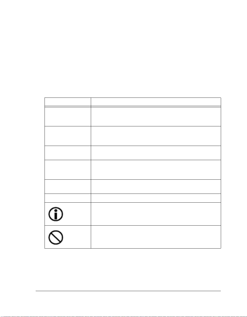
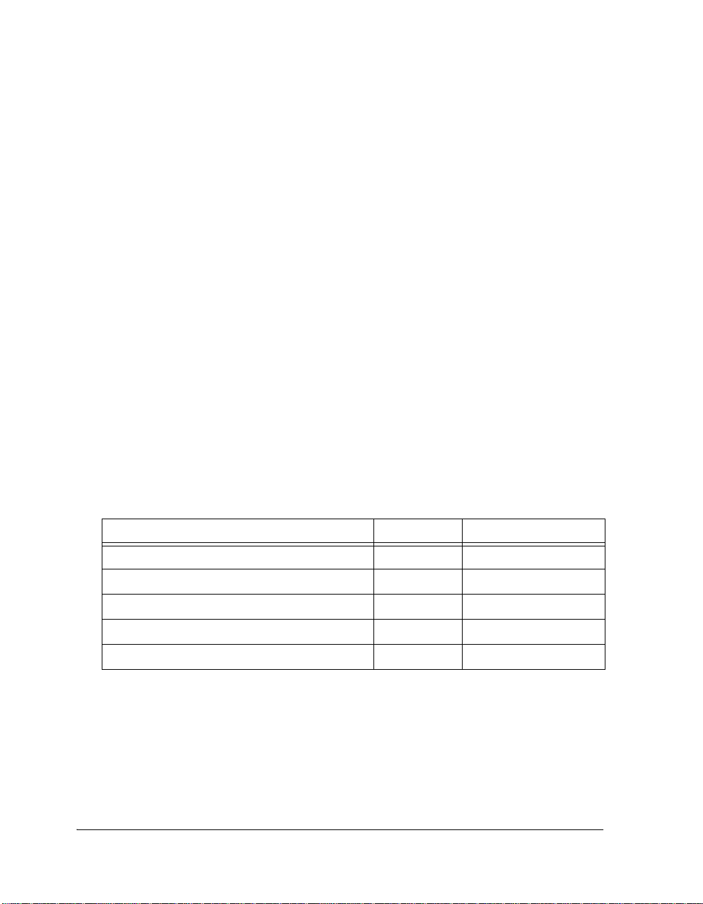
Notation Conventions
The following table identifies and describes text conventions used in this
manual.
Preface
!
Example Descriptio n
Close command
(File menu)
{this | that} Altern ative required items in syntax descriptions appear within curly
[this | that] Optional items in syntax descriptions appear within br ackets and s epa-
[this,…] Optional item lists in syntax descriptions appear within brackets
.SECTION Commands, directives, keywords, and feature names are in text with
filename Non-keyword placeholders appear in text with italic style format.
appear throughout this document.
Text in bold style indicates the location of an item within the
VisualDSP++ environment’s menu system. For example, the Close
command appears on the File menu.
brackets and separated by vertical bars; read the example as
that.
rated by vertical bars; read the example as an optional this or that.
delimited by commas and terminated with an ellipsis; read the example
as an optional comma-separated list of
letter gothic font.
A note, providing information of special interest or identifying a
related topic. In the online version of this book, the word Note appears
instead of this symbol.
this or
this.
Additional conventions, which apply only to specific chapters, may
A caution, providing information about critical design or programming issues that influence operation of a product. In the online version
of this book, the word Caution appears instead of this symbol.
Code has been formatted to fit this manual’s page width.
!
VisualDSP++ Loader Manual xix
for 16-Bit Processors
Page 20

Notation Conventions
xx VisualDSP++ Loader Manual
for 16-Bit Processors
Page 21

1 INTRODUCTION
The majority of this manual describes the loader program (or loader utility) as well as the process of loading and splitting, the final phase of a DSP
application program’s development flow. The process of initializing
on-chip and off-chip memories, is often referred to as booting.
The majority of this chapter applies to all 16-bit processors. Information
applicable to a particular target processor, or to a particular processor family, is provided in the following chapters.
• Chapter 2, “Blackfin Processor Loader/Splitter” on page 2-1
• Chapter 3, “ADSP-219x DSP Loader/Splitter” on page 3-1
• Chapter 4, “ADSP-2192-12 DSP Loader” on page 4-1
• Chapter 5, “ADSP-218x DSP Loader/Splitter” on page 5-1
Program Development Flow
The flow can be split into three phases:
1. “Compiling and Assembling”
2. “Linking”
3. “Loading and Splitting”
A brief description of each phase is as follows.
VisualDSP++ 3.5 Loader Manual 1-1
for 16-Bit Processors
Page 22

Program Development Flow
Compiling and Assembling
Input source files are compiled and assembled to yield object files. Source
files are text files containing C/C++ code, compiler directives, possibly a
mixture of assembly code and directives, and, typically, preprocessor commands. Refer to the VisualDSP++ 3.5 Assembler and Preprocessor Manual
or the VisualDSP++ 3.5 C/C++ Compiler and Library Manual for information about the assembler and compiler source files.
Linking
Under the direction of the Linker Description File (LDF) and linker settings, the linker consumes separately assembled object and library files to
yield an executable file. If specified, shared memory and overlay files are
also produced. The linker output conforms to the Executable and Linkable Format (ELF), an industry-standard format for executable files. The
linker also produces map files and other embedded information used by
the debugger (DWARF-2).
These executable files (.DXE) are not readable by the processor hardware
directly. They are neither supposed to be burned onto a EPROM or Flash
memory device. Executable files are consumed by VisualDSP++ debugging
targets, such as the simulator or emulator. Refer to the VisualDSP++ 3.5
Linker and Utilities Manual for 16-Bit Processors and online Help for information about linking and debugging.
Loading and Splitting
Upon completing the debug cycle, the processor hardware needs to run on
its own, without any debugging tools connected. After power-up, processor memories need to be initialized to be booted. Therefore, the linker
output must be transformed to a format readable by the processor. This
process is handled by the loader/splitter utility. The loader/splitter uses
the debugged and tested executable as well as shared memory and overlay
files as inputs to yield a processor-loadable file.
1-2 VisualDSP++ 3.5 Loader Manual
for 16-Bit Processors
Page 23

Introduction
VisualDSP++ includes two loader/splitter programs:
• elfloader.exe for ADSP-BF5xx and ADSP-219x processors
• elfspl21.exe for ADSP-218x processors
You can run the loader/splitter from the IDDE. In order to do so, change
you project’s type from DSP Executable to DSP Loader File. If preferred,
the command-line interface is also available.
Loader operations depend on loader options, which control how the
loader processes executable files, letting you select features such as kernels,
boot modes, and output file formats. These options are set on the Load
page of the Project Options dialog box in the VisualDSP++ environment
or on the loader’s command line. Option settings on the Load page corre-
spond to switches typed on the command line.
The loader/splitter output is either a boot-loadable or non-bootable file
(described in the following “Boot-loadable Files Versus Non-bootable
Files”). The output is meant to be loaded onto the target. There are sev-
eral ways to use the output:
• Download the loadable file into the processor’s PROM space on an
EZ-KIT Lite board via the Flash Programmer plug-in. Refer to
VisualDSP++ Help or the EZ-KIT Lite Evaluation System Manual
for information on the Flash Programmer.
• Use VisualDSP++ to simulate booting in a simulator session (where
supported). Load the loader file and then reset the processor to
debug the booting routines. No hardware is required: just point to
VisualDSP++ 3.5 Loader Manual 1-3
for 16-Bit Processors
Page 24

Program Development Flow
the location of the loader file, letting the simulator to do the rest.
You can step through the boot kernel code as it brings the rest of
the code into memory.
• Store the loader file in an array on a multiprocessor system. A master (host) processor has the array in its memory, allowing a full
control to reset and load the file into the memory of a slave
processor.
Boot-loadable Files Versus Non-bootable Files
A boot-loadable file is transported into and run from a processor’s internal
memory (on-chip boot ROM). (Note: This is different for ADSP-218x
processors.) The file is then programmed (burned) into an external memory device within your target system. The loader outputs files in
industry-standard file formats, such as Intel hex-32 and Motorola S,
which are readable by most EPROM burners. For advanced usage, other
file formats are supported.
A non-bootable EPROM-image file executes from the processor’s external
memory, bypassing the build-in boot mechanisms. Preparing a non-bootable EPROM image is called splitting. In most cases, developers working
with 16-bit processors use the loader instead of the splitter.
A processor’s booting sequence and an application program’s design dictate the way you call the loader/splitter programs to consume and
transform executables. For 16-bit processors, splitter and loader features
are handled by a single program. The splitter is invoked by a completely
different set of command-line switches than the loader. Refer to the guide
sections of the following chapters for information about splitting.
1-4 VisualDSP++ 3.5 Loader Manual
for 16-Bit Processors
Page 25

Introduction
Booting Modes
A fully debugged program can be automatically downloaded to the processor after power-up or after a software reset. This process is called booting.
The way the loader creates a boot-loadable file depends upon how your
program is booted into the processor.
Once an executable is fully debugged, it is ready to be converted into a
processor-loadable file.
The exact boot mode of the processor is determined by sampling one or
more of input flag pins. Booting sequences, highly processor-specific, are
detailed in the following chapters.
ADSP-218x, ADSP-219x, and Blackfin processors support different boot
mechanisms. Generally spoken, the following schemes can be used to provide program instructions to the processors after reset.
• “No-boot Mode”
• “PROM Booting Mode”
• “Host Booting Mode”
No-boot Mode
The processors starts fetching and executing instructions from
EPROM/Flash memory devices directly. This scheme does not require any
loader mechanism. It is up to the user program to initialize volatile
memories.
The splitter utility helps to generate a file that can be burned into the
PROM memory.
VisualDSP++ 3.5 Loader Manual 1-5
for 16-Bit Processors
Page 26

Booting Modes
PROM Booting Mode
After reset, the processor starts reading data from any parallel or serial
PROM device. The PROM stores a formatted boot stream rather than raw
instruction code. Beside application data, the boot stream contains additional data, such as destination addresses and word counts. A small
program called kernel or loader kernel (described on page 1-7) parses the
boot stream and initializes memories accordingly. The loader kernel runs
on the target processors. Depending on the architecture, the loader kernel
may execute from on-chip boot ROM or may be pre-loaded from the
PROM device into on-chip SRAM and execute from there.
The loader utility generates the boot stream from the linker’s executable
file and stores it to file format that can be burned into the PROM.
Host Booting Mode
In this scheme, the target processor is slave to a host system. After reset,
the processor delays program execution until it gets signalled by the host
system that the boot process has completed. Depending on hardware capabilities, there are two different methods of host booting. In the first case,
the host system has full control over all target memories. It halts the target
while it is initializing all memories as required. In the second case, the
host communicates by a certain handshake with the loader kernel running
on the target processor. This kernel may execute from on-chip ROM or
may be pre-loaded by the host devices into the target’s SRAM by any
boot-strapping scheme.
The loader/splitter utility generates a file that can be consumed by the
host device. It depends on the intelligence of the host device and on the
target architecture whether the host expects raw application data or a formatted boot stream.
1-6 VisualDSP++ 3.5 Loader Manual
for 16-Bit Processors
Page 27

Introduction
In this context, a boot-loadable file is a file that stores instruction code in
a formatted manner in order to be processed by a boot kernel. A
non-bootable file stores raw instruction code. Note that in some case, a
single file may contain both types of data.
Boot Kernels
A (loader) boot kernel refers to the resident program in the boot ROM
space responsible for booting the processor. Alternatively (or in absence of
the boot ROM), the boot kernel can be pre-loaded from the boot source
by a boot-strapping scheme.
When a reset signal is sent to the processor, the processor starts booting
from a PROM, host device, or through a communication port. For example, a ADSP-218x/219x processor brings a 256-word program in internal
memory for execution. This small program is called a boot kernel. The
boot kernel then brings the rest of the booting routines into the processor’s memory. Finally, the boot kernel overwrites itself with the final block
and jumps to the beginning of the application program.
On the ADSP-219x DSPs, the highest 16 locations in page 0 program
memory and the highest 272 locations in page 0 data memory are reserved
for use by the ROM boot routines (typically for setting up DMA data
structures and for bookkeeping operations). Ensure that the boot sequence
entry code or boot-loaded program do not need to initialize this space at
boot time. However, the program can use these locations at run-time.
Some of the newer Blackfin processors (ADSP-BF531, ADSP-BF532, and
ADSP-BF533) do not require a boot kernel: the advanced on-chip boot
ROM allows the entire application program body to be booted into the
internal memory of the processor. The on-chip boot ROM for the former
processors behaves similar to the second-stage loader of ADSP-BF535 processors. The boot ROM has the capability to parse address and count
information for each bootable block.
VisualDSP++ 3.5 Loader Manual 1-7
for 16-Bit Processors
Page 28

Loader Tasks
Loader Tasks
Common tasks perform by the loader include:
• Processing loader option settings or command-line switches.
• Formatting the output .LDR file according to user specifications.
Supported formats are binary, ASCII, hex-32, and more. Valid file
formats are described in Appendix A on page A-1.
• Packing the code for a particular data format: 8- or 16-bit.
• If specified, adding a boot kernel on top of the user code.
• If specified, preprogramming the location of the .LDR file in
PROM space.
• Specifying processor IDs for multiple input .DXEs for a multiprocessor system.
Loader Files
The loader/splitter output is essentially the same executable code as in the
input .DXE file. The loader repackages the executable, as illustrated in
Figure 1-1.
Processor code in a loader file is split into blocks. Each code block is
marked with a tag that contains information about the block, such as a
number of words or destination in processor’s memory. Depending on the
processor family, there may be additional information in the tag. Common block types are “zero” (memory is filled with 0s); non-zero (code or
data); and final (code or data). Depending on the processor family, there
may be other block types.
1-8 VisualDSP++ 3.5 Loader Manual
for 16-Bit Processors
Page 29
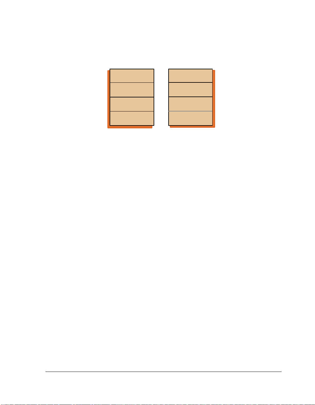
Introduction
.LDR File
Code
Data
Symbols
DebugInformation
An .LDR file includes:
DSPinstructions (codeand
data)
Rudimentary formatting
All ofthedebugginginformation
has been taken out of the file
A .DXE file includes:
Symboltable andsection
information
Targetprocessor's memory
layout
Degugging information
Code instru ct io ns
.DXE File
Code
Data
Symbols
Debug Information
Figure 1-1. .DXE Files versus .LDR Files
File Searches
File searches are important in the loader operation. The loader supports
relative and absolute directory names, default directories. File searches
occur as follows.
• Specified path—If you include relative or absolute path information in a file name, the loader searches only in that location for the
file.
• Default directory—If you do not include path information in the
file name, the loader searches for the file in the current working
directory.
• Overlay and shared memory files—the loader recognizes overlay
memory files but does not expect these files on the command line.
Place the files in the same directory as the executable file that refers
to them. The loader can locate them when processing the
executable.
VisualDSP++ 3.5 Loader Manual 1-9
for 16-Bit Processors
Page 30

Loader Files
When providing an input or output file as a loader/splitter command-line
parameter, use the following guidelines.
• Enclose long file names within straight quotes, “long file name”.
• Append the appropriate file extension to each file.
1-10 VisualDSP++ 3.5 Loader Manual
for 16-Bit Processors
Page 31

2 BLACKFIN PROCESSOR
LOADER/SPLITTER
This chapter explains how the loader/splitter program (elfloader.exe) is
used to convert executable files (.DXE) into boot-loadable or non-bootable
files for the ADSP-BF5xx Blackfin processors.
Refer to “Introduction” on page 1-1 for the loader overview; the introduc-
tory material applies to all processor families. Loader operations specific to
ADSP-BF5xx Blackfin processors are detailed in the following sections.
• “Blackfin Processor Booting” on page 2-2
Provides general information on various booting modes, including
information on second-stage kernels:
• “ADSP-BF535 Processor Booting” on page 2-3
• “ADSP-BF531/BF532/BF533 Processor Booting” on
page 2-16
• “ADSP-BF561 Processor Booting” on page 2-28
• “Blackfin Processor Loader Guide” on page 2-40
Provides reference information on the loader’s command-line syn-
tax and switches.
VisualDSP++ Loader Manual 2-1
for 16-Bit Processors
Page 32

Blackfin Processor Booting
Blackfin Processor Booting
Figure 2-1 is a simplified view of the Blackfin processor’s booting
sequence.
Source Files
.ASM, .C,.CPP
Assembler
and/or
Compiler
ADSP-BF53x
Processor
.DOJ
Target System
Booting
upon
RESET
Linker
External
Memory
.DXE
Loader
.LDR
Figure 2-1. Blackfin Processors: Booting Sequence
A Blackfin processor can be booted from an 8- or 16-bit Flash/PROM
memory or an 8-,16-, or 24-bit addressable SPI memory. (24-bit addressable SPI memory booting supported only on ADSP-BF531/BF532/BF533
processors.) There is also a no-boot option (bypass mode), in which execution occurs from a 16-bit external memory.
At powerup, after the reset, the processor transitions into a boot mode
sequence configured by the
bits in the System Reset Configuration Register (
BMODE pins. These pins can be read through
SYSCR). The BMODE pins
are dedicated mode-control pins; that is, no other functions are shared
with these pins.
2-2 VisualDSP++ Loader Manual
for 16-Bit Processors
Page 33

Blackfin Processor Loader/Splitter
!
information on system configuration, peripherals, registers, and
operating modes.
ADSP-BF535 Processor Booting
Upon reset, an ADSP-BF535 processor jumps to an external 16-bit mem-
Refer to the processor’s data sheet and Hardware Reference for more
ory for execution (if
BMODE = 001, 010, 011). Table 2-1 summarizes booting modes and code
execution start addresses for ADSP-BF535 processors.
Table 2-1. ADSP-BF535 Processor Boot Mode Selections
Boot Source BMODE[2:0] Execution Start Address
Execute from 16-bit external memory (Async Bank 0);
no-boot mode (bypass on-chip boot ROM)
Boot from 8-bit/16-bit Flash memory 001
Boot from 8-bit address SPI0 serial EEPROM 010
Boot from 16-bit address SPI0 serial EEPROM 011
Reserve d 111—100 N/A
BMODE = 000) or to the on-chip boot ROM (if
000 0x2000 0000
0xF000 0000
0xF000 0000
0xF000 0000
1
1
1
1 The processor jumps to this location after the booting is complete.
A description of each boot mode is as follows.
• “ADSP-BF535 Processor On-Chip Boot ROM” on page 2-4
• “ADSP-BF535 Processor Second-Stage Loader” on page 2-6
• “ADSP-BF535 Processor Boot Streams” on page 2-8
• “ADSP-BF535 Processor Memory Ranges” on page 2-13
VisualDSP++ Loader Manual 2-3
for 16-Bit Processors
Page 34

Blackfin Processor Booting
ADSP-BF535 Processor On-Chip Boot ROM
The on-chip boot ROM for the ADSP-BF535 processor does the following (Figure 2-2).
ADSP-BF535 Processor
0xEF00 0000
On-Chip
Boot ROM
L2 Memory
(0xF000 0000)
4-Byte Header (N)
0x0
2ndStage Loader
2ndStage Loader
or
or
Application
Application
Code
Code
2ndStage Loader
or
Application
Code
PROM/Flash or SPI Device
N
Bytes
Figure 2-2. ADSP-BF535 Processors: On-Chip Boot ROM
1. Sets up Supervisor mode by exiting the RESET interrupt service routine and jumping into the lowest priority interrupt (IVG15).
2. Checks whether the RESET was a software reset and if so, whether to
skip the entire boot sequence and jump to the start of L2 memory
0xF000 0000) for execution. The on-chip boot ROM does this by
(
checking bit 4 of the
SYSCR. If bit 4 is not set, the on-chip boot
ROM performs the full boot sequence. If bit 4 is set, the on-chip
boot ROM bypasses the full boot sequence and jumps to 0xF000
0000
. The register settings are shown in Figure 2-3.
2-4 VisualDSP++ Loader Manual
for 16-Bit Processors
Page 35

Blackfin Processor Loader/Splitter
System Reset Configuration Register (SYSCR)
X - state is initialized from mode pins during hardware reset
15 14 13 12 11 10 9 8 7 6 5 4 3 2 1 0
000000000000XXX
0
Reset = dependent on pin values
No Boot on Software Reset
0 - Use BMODE to determine
boot source.
1 - Start executing from the
beginning of on-chip L2 memory
(or the beginning of ASYNC Bank 0
when BMODE[2:0] = b#000).
BMODE 2-0 - RO
000 - Bypass boot ROM,
execute from 16-bit-wide
external memory.
001 - Use boot ROM to load
from 8-bit/16-bit FLASH.
010 - Use boot ROM to configure
and load boot code from
SPI0 serial ROM
(8-bit address rang e).
011 - Use boot ROM to configure
and load boot code from
SPI0 serial ROM
(16-bit address range).
100-111 - Reserved
Figure 2-3. ADSP-BF535 Processors: System Reset Configuration Register
3. Finally, if bit 4 of the SYSCR register is not set, the on-chip boot
ROM performs the full boot sequence. The full boot sequence
includes:
" Checking the boot source (either Flash/PROM or SPI mem-
ory) by reading BMODE[2:0] from the SYSCR register.
" Reading the first four bytes from location 0x0 of the exter-
nal memory device. These four bytes contain the byte count
(
N), which specifies the number of bytes to boot in.
" Booting in N bytes into internal L2 memory starting at loca-
0xF000 0000.
tion
" Jumping to the start of L2 memory for execution.
The on-chip boot ROM boots in N bytes from the external memory. These
N bytes can define the size of the actual application code or a second-stage
loader (boot kernel) that boots in the application code.
VisualDSP++ Loader Manual 2-5
for 16-Bit Processors
Page 36

Blackfin Processor Booting
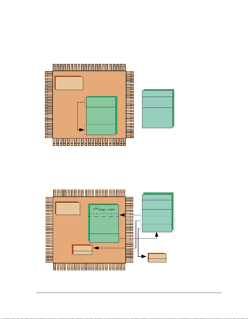
ADSP-BF535 Processor Second-Stage Loader
The only situation where a second-stage loader is unnecessary is when the
application code contains only one section starting at the beginning of L2
memory (0xF000 0000).
A second-stage loader must be used in applications in which multiple segments reside in L2 memory or in L1 memory and/or SDRAM. In
addition, a second-stage loader must be used to change the wait states or
hold time cycles for a Flash/PROM booting or to change the baud rate for
a SPI boot (see “Command-Line Switches” on page 2-42 for more information on these features).
When a second-stage loader is used for booting, the following sequence
takes place.
1. Upon RESET, the on-chip boot ROM downloads N bytes (the
second-stage loader) from external memory to address 0xF000 0000
in L2 memory (Figure 2-4).
ADSP-BF535 Processor
0xEF00 0000
On-Chip
Boot ROM
L2 Memory
(0xF000 0000)
2ndStage Loader
2ndStage Loader
or
Application
Code
4-ByteHeader (N)
2ndStageL oader
Application
Code/Data
PROM/Flash or SPI Device
0x0
Bytes
N
Figure 2-4. ADSP-BF535 Processors: Booting With Second-Stage Loader
2-6 VisualDSP++ Loader Manual
for 16-Bit Processors
Page 37
Blackfin Processor Loader/Splitter
2. The second-stage loader copies itself to the bottom of L2 memory.
ADSP-BF535 Processor
0xEF00 0000
On-Chip
Boot ROM
L2 Memory
(0xF000 0000)
2ndStage Loader
2ndStage Loader
or
Application
Code
2ndStage Loader
PROM/Flashor SPI Device
4-Byte Header (N)
2ndStage Loader
Application
Code/Data
0x0
Figure 2-5. ADSP-BF535 Processors: Copying Second-Stage Loader
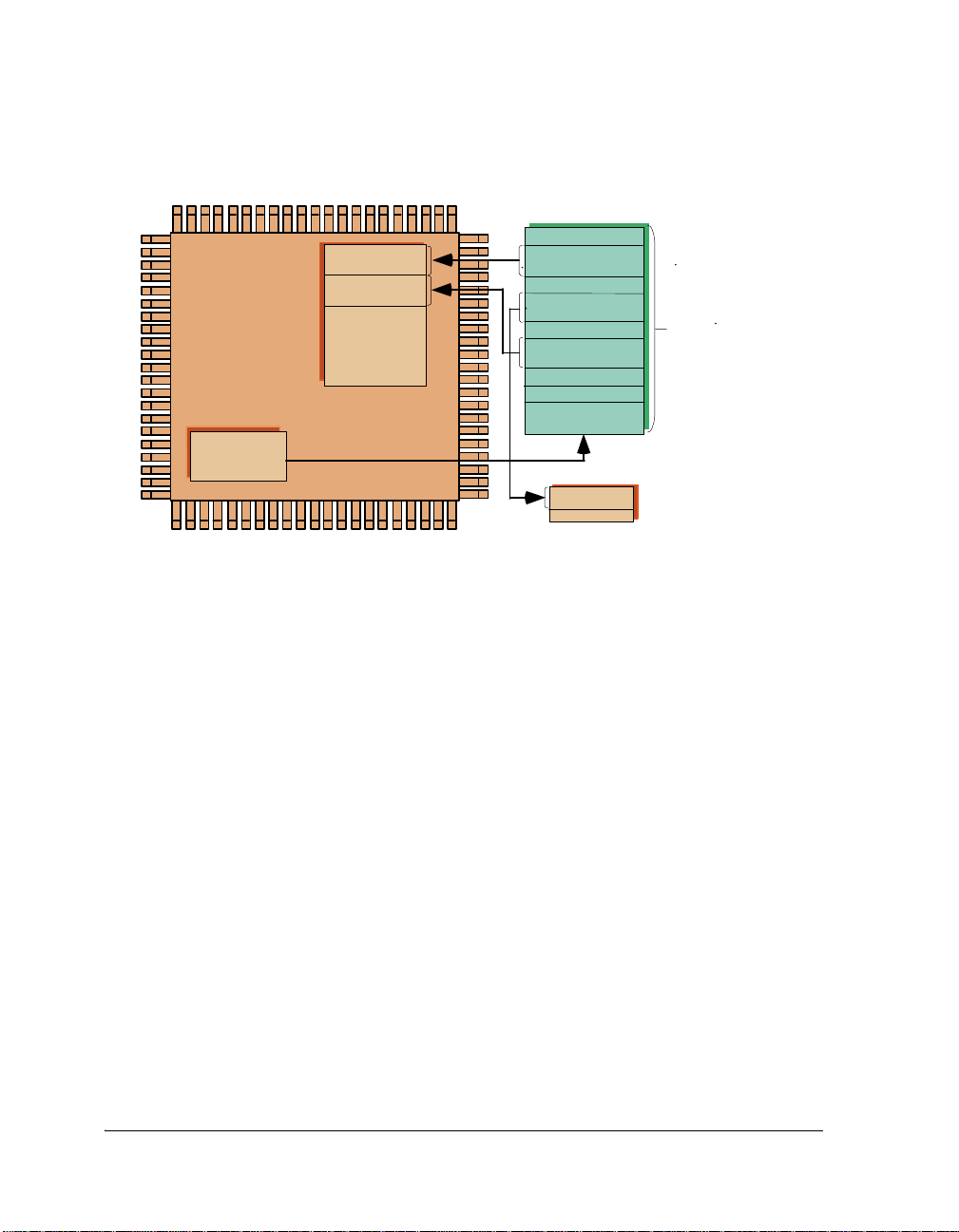
3. The second-stage loader boots in the application code/data into the
various memories of the Blackfin processor.
ADSP-BF535 Processor
0xEF00 0000
On-Chip
Boot ROM
L1 Memory
B
L2 Memory
(0x F000 0000 )
A
2ndStage Loader
or
Application
2ndStage Loader
Code
PROM/Flash or SPI Device
4-B yteHeader (N)
2ndStage Loader
A
B
C
SDRAM
C
0x0
Application
Code/Data
Figure 2-6. ADSP-BF535 Processors: Booting Application Code
VisualDSP++ Loader Manual 2-7
for 16-Bit Processors
Page 38

Blackfin Processor Booting
4. Finally, after booting, the second-stage loader jumps to the start of
L2 memory (0xF000 0000) for application code execution
(Figure 2-7).
ADSP-BF535 Processor
0xEF00 0000
On-Chip
Boot ROM
L1 Memory
B
L2 Memory
(0xF000 0000)
A
2ndStage Loader
PROM/Flash or SPI Device
4-ByteHeader (N)
2nd S tage Loader
A
B
C
SDRAM
C
0x0
Application
Code/Data
Figure 2-7. ADSP-BF535 Processors: Starting Application Code
ADSP-BF535 Processor Boot Streams
The loader generates the boot stream and places the boot stream in the
output loader file (.LDR). The loader prepares the boot stream in such a
way that the on-chip boot ROM and the second-stage loader can correctly
load the application code and data to the processor memory. Therefore,
the boot stream contains not only the user application code but also
header and flag information that is used by the on-chip boot ROM and
the second-stage loader.
2-8 VisualDSP++ Loader Manual
for 16-Bit Processors
Page 39

Blackfin Processor Loader/Splitter
Diagrams in this section illustrate boot streams utilized by the
ADSP-BF535 processor’s boot kernel. The elements are covered as
follows.
• “Output Loader Files” on page 2-9
• “Global Headers” on page 2-12
• “Block Headers” on page 2-13
• “Flags” on page 2-13
Output Loader Files
An output loader file for 8-bit PROM/Flash booting and 8-/16-bit
addressable SPI booting without the second-stage loader:
Output .LDR File
4-Byte Headerfor
Byte Count (N)
Byte 0
Byte Count for
Application Code
Byte 1
Byte 2
Byte 3
........
........
........
D7
Application
Code
D0
VisualDSP++ Loader Manual 2-9
for 16-Bit Processors
Page 40

Blackfin Processor Booting
An output loader file for 16-bit PROM/Flash booting without the second-stage loader:
Output .LDR File
0x00
0x00
0x00
4-Byte Header for
Byte Count (N)
Byte 0
Byte 1
Byte Count for
nd
Stage Loader
2
0x00
0x00
0x00
0x00
0x00
D15 D8 D7 D0
Byte 2
Byte 3
........
........
........
Application
Code
(N words)
An output loader file for 8-bit PROM/Flash booting and 8- or 16-bit
addressable SPI booting with the second-stage loader or kernel:
Output .LDR File
4-ByteHeader for
Byte Count(N)
Byte0
Byte1
Byte2
........
Byte0
Byte1
Byte 2
........
D7
Byte Count for
nd
Stage Loader
2
2ndStage Loader
(N Bytes)
Application
Code
(in blocks)
D0
2-10 VisualDSP++ Loader Manual
for 16-Bit Processors
Page 41

Blackfin Processor Loader/Splitter
An output loader file for 16-bit PROM/FLASH booting with the second-stage loader or kernel:
Output .LDR File
0x00
0x00
0x00
0x00
0x00
4-ByteHeader for
Byte Count (N)
Byte 0
Byte 1
Byte 2
........
Byte Count for
nd
Stage Loader
2
2ndStage Loader
Byte 1
Byte 3
Byte 5
........
D15 D8 D7 D0
Byte 0
Byte 2
Byte 4
........
Application
Code
(in blocks)
Global Headers and Blocks
Following kernel code and kernel address in a loader file, there is a 4-byte
global header. The header provides the global settings for a booting
process:
Output .LDR File
4Bytes
NBytes
4Bytes
4Bytes
4Bytes
Byte Count(N)
nd
2
Stage Loader
2nd Stag e Load er
Address
Global Header
Size ofApplication
Code (N1)
Byte Count for
nd
2
Stage Loader
Address ofthe Bottom of L2 Memory
from which 2
See "Global Header"
nd
Stage Loader runs
N1 Bytes
Application Code
VisualDSP++ Loader Manual 2-11
for 16-Bit Processors
Page 42

Blackfin Processor Booting
A block is the basic structure of the output .LDR file for application code
when the second-stage loader is used. All the application code is grouped
into blocks. A block always has a block header an a block body if it is a
non-zero block. A block does not have a block body if it is a zero block. A
block header is illustrated below:
4Bytes
NBytes
4Bytes
4Bytes
4Bytes
N1 Bytes
Output .LDR File
Byte Count (N)
nd
Stage Loader
2
2nd S tageLoader
Address
Global H ead er
Size of Application
Code (N1)
Applicatio n Code
Size ofApplication
Code (N1)
Start Address
of Block 1
Byte Count
of Block 1
Flag for Block 1
Body of Block 1
Start Address
of Block 2
Byte Count
of Block 2
......
4Bytes
4Bytes
2Bytes
Global Headers
A global header for 8- and 16-bit PROM/Flash booting:
015 14 13 12 11 10 9 8 7 6 5
Number of hold time cycles: 3 (default)
Number of wait states: 15 (default)
1 = 16-bit PROM/Flash, 0 = 8-bit PROM/Flash: 0 (default)
321
4
Block
Header
Block
A global header for 8- and 16-bit addressable SPI booting:
015 14 13 12 11 10 9 8 7 6 5
Baud rate: 0 = 500 kHz (default), 1 = 1 MHz, 2 = 2 MHz
321
4
2-12 VisualDSP++ Loader Manual
for 16-Bit Processors
Page 43

Blackfin Processor Loader/Splitter
Block He ad er s
A block header has three words: 4-byte clock start address, 4-byte block
byte count, and 2-byte flag word.
Flags
The ADSP-BF535 block flag word’s bits are illustrated below.
015 14 13 12 11 10 9 8 7 6 5
Bit 15: 1 = Last Block, 0 = No t La st Bl ock
321
4
Bit 0: 1 = Zero Fill, 0 = No Zero Fill
ADSP-BF535 Processor Memory Ranges
Second-stage loaders are available for ADSP-BF535 processors in VisualDSP++ 3.0 and higher. They allow booting to:
• L2 memory (0xF000 0000)
• L1 memory
" Data Bank A SRAM (0xFF80 0000)
" Data Bank B SRAM (0xFF90 0000)
" Instruction SRAM (0xFFA0 0000)
" Scratchpad SRAM (0xFFB0 0000)
•SDRAM
" Bank 0 (0x0000 0000)
" Bank 1 (0x0800 0000)
VisualDSP++ Loader Manual 2-13
for 16-Bit Processors
Page 44

Blackfin Processor Booting
" Bank 2 (0x1000 0000)
" Bank 3 (0x1800 0000)
!
data are loaded into it.
For more information see “Using Second-Stage Loader” on page 2-49.
Second-Stage Loader Restrictions
When using the second-stage loader:
• The bottom of L2 memory must be reserved during booting. These
locations can be reallocated during runtime. The following locations pertain to the current second-stage loaders.
SDRAM must be initialized by user code before any instructions or
" For 8- and 16-bit PROM/Flash booting, reserve
0xF003 FE00–0xF003 FFFF (last 512 bytes).
" For 8- and 16-bit addressable SPI booting, reserve
0xF003 FD00–0xF003 FFFF (last 768 bytes).
• If segments reside in SDRAM memory, configure the SDRAM registers accordingly in the second-stage loader kernels before booting.
" Modify section of code called “SDRAM setup” in the
second-stage loader and rebuild the second-stage loader.
• Any segments residing in L1 instruction memory
(0xFFA0 0000–0xFFA0 3FFF) must be 8-byte aligned.
" Declare segments, within the .LDF file, that reside in L1
instruction memory at starting locations that are 8-byte
aligned (for example,
0xFFA0 0010, and so on).
" Or use the .ALIGN 8; directives in the application code.
0xFFA0 0000, 0xFFA0 0008,
2-14 VisualDSP++ Loader Manual
for 16-Bit Processors
Page 45

Blackfin Processor Loader/Splitter
!
The two reasons for this restriction are:
• Core writes into L1 instruction memory are not allowed.
• DMA from an 8-bit external memory is not possible since
the minimum width of the External Bus Interface Unit
(EBIU) is 16 bits.
Load bytes into L1 instruction memory by using the instruction test command and data registers, as described in the Memory chapter of the
appropriate Hardware Reference manual. These registers transfer 8-byte
sections of data from external memory to internal L1 instruction memory.
VisualDSP++ Loader Manual 2-15
for 16-Bit Processors
Page 46

Blackfin Processor Booting
ADSP-BF531/BF532/BF533 Processor Booting
Upon reset, an ADSP-BF531/BF532/BF533 processor jumps to the
on-chip boot ROM (if BMODE = 01, 11) or jumps to 16-bit external memory for execution (if BMODE = 00) located at 0xEF00 0000. Table 2-2 shows
booting modes and execution start addresses for ADSP-BF531,
ADSP-BF532, and ADSP-BF533 processors.
Table 2-2. ADSP-BF531/BF532/BF533 Processor Boot Mode Selections
Execution Start Address
Boot Source BMODE[1:0]
ADSP-BF531
ADSP-BF532
Processors
ADSP-BF533
Processor
Execute from 16-bit External ASYNC Bank0
memory (no-boot mode or bypass on-chip boot
ROM)
Boot from 8- or 16-bit Prom/Flash 01 0xFFA0 8000 0xFFA0 0000
Reserve d 10 0xFFA0 8000 0xFFA0 0000
Boot from a 8-, 16-, or 24-bit addressable SPI
memory
00 0x2000 0000 0x2000 0000
11 0xFFA0 8000 0xFFA0 0000
A description of each boot mode is as follows.
• “ADSP-BF531/BF532/BF533 Processor On-Chip Boot ROM” on
page 2-17
• “ADSP-BF531/BF532/BF533 Processor Boot Streams” on
page 2-19
2-16 VisualDSP++ Loader Manual
for 16-Bit Processors
Page 47

Blackfin Processor Loader/Splitter
ADSP-BF531/BF532/BF533 Processor On-Chip Boot ROM
The on-chip boot ROM for ADSP-BF531/BF532/BF533 processors does
the following.
1. Sets up supervisor mode by exiting the RESET interrupt service routine and jumping into the lowest priority interrupt (IVG15).
2. Checks whether the RESET was a software reset and if so, whether to
skip the entire boot sequence and jump to the start of L1 memory
(0xFFA0 0000 for ADSP-BF533 processor; 0xFFA0 8000 for
ADSP-BF531 and ADSP-BF532 processors) for execution. The
on-chip boot ROM does this by checking bit 4 of the System Reset
Configuration Register (Figure 2-8). If bit 4 is not set, the on-chip
boot ROM performs the full boot sequence. If bit 4 is set, the
on-chip boot ROM bypasses the full boot sequence and jumps to
the start of L1 memory.
System Reset Configuration Register (SYSCR)
X - state is initialized from mode pins during hardware reset
0xFFC0 0104
No Boot on Software Reset
0 - Use BMODE to determine
boot source
1 - Start executing from the
beginning of on-chip L1
memory or the beginning of
ASYNC Bank 0 when
BMODE[1:0] = b#00
15 14 13 12 11 10 9 8 7 6 5 4 3 2 1 0
0 000000 0 XX
Reset = dependent on pin
values
00000 0
BMODE[1:0] (Boot Mode)- RO
00 - Bypass boot ROM,
execute from 16-bit
external memory
01 - Use boot ROM to load
from 8-bit flash
10 - Use boot ROM to configure
and load boot code from
SPI serial ROM
(8-bit address range)
11 - Use boot ROM to configure
and load boot code from
SPI serial ROM
(16-bit address range)
Figure 2-8. ADSP-BF533 Processors: System Reset Configuration Register
3. Eventually, if bit 4 of the SYSCR register is not set, the on-chip boot
ROM performs the full boot sequence (Figure 2-9).
VisualDSP++ Loader Manual 2-17
for 16-Bit Processors
Page 48
Blackfin Processor Booting
ADSP-BF531/BF532/BF533 Processor
L1 Memory
0xEF00 0000
On-Chip
BootROM
Block 1
Block 3
........
A
PROM/Flash or SPI Device
10-Byte Header for Block 1
Block 1
10-Byte Header for Block 2
Block 2
10-ByteHeaderforBlock3
Block 3
........
10-Byte Header for Block n
Block n
SDRAM
Block 2
App.
Code/
Data
Figure 2-9. ADSP-BF531/BF532/BF533 Processors: Booting Sequence
The booting sequence for ADSP-BF531, ADSP-BF532, and
ADSP-BF533 processors is quite different from that of ADSP-BF535 processors. The on-chip boot ROM for the former processors behaves similar
to the second-stage loader of ADSP-BF535 processors. The boot ROM
has the capability to parse address and count information for each bootable block. This alleviates the need for a second-stage loader for
ADSP-BF531/BF532/BF533 processors because a full application can be
booted to the various memories with just the on-chip boot ROM.
The loader converts the application code (.DXE) into the loadable file by
parsing the code and creating a file that consists of different blocks. Each
block is encapsulated within a 10-byte header which is illustrated in
Figure 2-9 and detailed in the following section. These headers, in turn,
are read and parsed by the on-chip boot ROM during booting. The
10-byte header provides all the information the on-chip boot ROM
requires: where to boot the block to, how many bytes to boot in, and what
to do with the block.
2-18 VisualDSP++ Loader Manual
for 16-Bit Processors
Page 49

Blackfin Processor Loader/Splitter
ADSP-BF531/BF532/BF533 Processor Boot Streams
The following sections describe the boot stream, header, and flag framework for ADSP-BF531, ADSP-BF532, and ADSP-BF533 processors.
• “Blocks and Block Headers” on page 2-19
• “Flags of Block Header” on page 2-20
• “Initialization Blocks” on page 2-21
The ADSP-BF531/BF532/BF533 processor boot stream is similar to the
boot stream that uses a second-stage kernel of ADSP-BF535 processors
(detailed in “ADSP-BF535 Processor Boot Streams” on page 2-8). However, since the former processors do not employ a kernel, their boot
streams do not include the kernel code and the associated 4-byte header
on the top of the kernel code. There is also no 4-byte global header.
Blocks and Block Headers
As the loader converts the code from an input .DXE file into blocks comprising the output loader file, each block is getting preceded by a 10-byte
header (Figure 2-10), followed by a block body (if it is a non-zero block)
or no block body (if it is a zero block). A description of the header structure can be found in Table 2-3.
Table 2-3. ADSP-BF531/BF532/BF533 Block Header Structure
Bit Field Description
Address 4-byte address at which the block resides in memory.
Count 4-byte number of bytes to boot.
Flag 2-byte flag containing information about the block “Flags of Block
Header” on page 2-20 describes the flag structure.
VisualDSP++ Loader Manual 2-19
for 16-Bit Processors
Page 50

Blackfin Processor Booting
Block
Header for DX E1 Count
DXE1 ByteCount
Header for Block1
Block1
Header for Block2
Block2
......
......
Headerfor DXE2 Count
DXE2 ByteCount
......
......
10-Byte Header
4-Byte Addr ess
4-Byte Count
2-Byte Flag
See F lag Informa tion
Figure 2-10.
ADSP-BF531/BF532/BF533 Processor Boot Stream Structur
Flags of Block Header
Refer to the following figure and Table 2-4 for the flag’s bit descriptions.
015 14 13 12 11 10 9 8 7 6 5
Last Block:
1 = last block, 0 = not last block
Ignore Block: 1 = ignore block, 0 = do not ignore block
Initialization Block: 1 = init block, 0 = non-init block
Processor Type: 1 = ADSP-BF533
0 = ADSP-BF531/BF532
Zero-Fill: 1 = zero fill block, 0 = non-zero fill block
Bits 14–5 are reserved for future use
321
4
e
2-20 VisualDSP++ Loader Manual
for 16-Bit Processors
Page 51

Blackfin Processor Loader/Splitter
Table 2-4. Flag Structure
Bit Field Description
Zero-Fill Block Indicates that the block is a buffer filled with zeros. Zero Block is not included
within loader file. When the loader parses through the .DXE file and encounters
a large buffer with zeros, it creates a zero-fill block to reduce .LDR file size and
boot time. If this bit is set, there is no data in the block.
Ignore Block Indicates that the block is not to be booted into memory; skips the block and
move on to the next one. Currently is not implemented for application code.
Initialization
Block
Processor Type Indicates the processor, either ADSP-BF531/BF532 or ADSP-BF533. After
Last Block Indicates that the block is the last block to be booted into memory. After the
Indicates that the block is to be executed before booting. The initialization
block indicator allows the on-chip boot ROM to execute a number of instructions before booting the actual application code. When the on-chip boot ROM
detects an Init Block, it boots the block into internal memory and makes a
CALL to it (Initialization code must have a RTS at the end).
This option allows the user to run initialization code (such as SDRAM initialization) before the full boot sequence proceeds. Figure 2-11 and Figure 2-12
illustrate the process. Initialization code can be included within the .LDR file by
using the
booting is complete, the cn-chip boot ROM jumps to 0xFFA0 0000 for a
ADSP-BF533 processor and to 0xFFA0 8000 for a ADSP-BF531/BF532 processor.
last block, the processor jumps to the start of L1 memory for application code
execution. When it jumps to L1 memory for code execution, the processor is
still in Supervisor Mode and in the lowest priority interrupt (IVG15).
-init switch (see “-init filename” on page 2-43).
Initialization Blocks
The -init filename option directs the loader to produce an initialization
block from the code of the initialization section of the named file. The initialization block is placed at the top of a loader file. It is executed before
the rest of the code in the loader file is booted into the memory (see
Figure 2-11).
Following execution of the initialization block, the booting process continues with the rest of data blocks until it encounters a final block (see
Figure 2-12). The initialization code example follows in Listing 2-1
VisualDSP++ Loader Manual 2-21
for 16-Bit Processors
Page 52

Blackfin Processor Booting
ADSP-BF531/BF532/BF533 Processor
L1 Memory
0xEF00 0000
On-Chip
BootROM
Init Block
A
PROM/Flash or SPI Device
Headerfor Init Block
Init Block
1eaderfor L1 Block
L1 Block
Header for SDRAM Block
SDRAM Block
........
10-Byte Header for Block n
Block n
SDRAM
App.
Code/
Data
Figure 2-11. ADSP-BF531/BF532/BF533: Initialization Block Execution
Figure 2-12. ADSP-BF531/BF532/BF533: Booting Application Code
2-22 VisualDSP++ Loader Manual
for 16-Bit Processors
Page 53

Blackfin Processor Loader/Splitter
Listing 2-1. Initialization Block Code Example
/* This file contains 3 sections: */
/* 1) A Pre-Init Section–this section saves off all the
DSP registers onto the stack.
2) An Init Code Section–this section is the initialization
code which can be modified by the customer
As an example, an SDRAM initialization code is supplied.
The example setups the SDRAM controller as required by
certain SDRAM types. Different SDRAMs may require
different initialization procedure or values.
3) A Post-Init Section–this section restores all the register
from the stack. Customers should not modify the Pre-Init
and Post-Init Sections. The Init Code Section can be
modified for a particular application.*/
#include <defBF532.h>
.SECTION program;
/**********************Pre-Init Section************************/
[--SP] = ASTAT; /* Stack Pointer (SP) is set to the end of */
[--SP] = RETS; /* scratchpad memory (0xFFB00FFC) */
[--SP] = (r7:0); /* by the on-chip boot ROM */
[--SP] = (p5:0);
[--SP] = I0;[--SP] = I1;[--SP] = I2;[--SP] = I3;
[--SP] = B0;[--SP] = B1;[--SP] = B2;[--SP] = B3;
[--SP] = M0;[--SP] = M1;[--SP] = M2;[--SP] = M3;
[--SP] = L0;[--SP] = L1;[--SP] = L2;[--SP] = L3;
/*******************Init Code Section**************************/
/*******Please insert Initialization code in this section******/
/***********************SDRAM Setup****************************/
Setup_SDRAM:
P0.L = EBIU_SDRRC & 0xFFFF;
/* SDRAM Refresh Rate Control Register */
VisualDSP++ Loader Manual 2-23
for 16-Bit Processors
Page 54

Blackfin Processor Booting
P0.H = (EBIU_SDRRC >> 16) & 0xFFFF;
R0 = 0x074A(Z);
W[P0] = R0;
SSYNC;
P0.L = EBIU_SDBCTL & 0xFFFF;
/* SDRAM Memory Bank Control Register */
P0.H = (EBIU_SDBCTL >> 16) & 0xFFFF;
R0 = 0x0001(Z);
W[P0] = R0;
SSYNC;
P0.L = EBIU_SDGCTL & 0xFFFF;
/* SDRAM Memory Global Control Register */
P0.H = (EBIU_SDGCTL >> 16) & 0xFFFF;//
R0.L = 0x998D;
R0.H = 0x0091;
[P0] = R0;
SSYNC;
/*********************Post-Init Section************************/
L3 = [SP++]; L2 = [SP++]; L1 = [SP++]; L0 = [SP++];
M3 = [SP++]; M2 = [SP++]; M1 = [SP++]; M0 = [SP++];
B3 = [SP++]; B2 = [SP++]; B1 = [SP++]; B0 = [SP++];
I3 = [SP++]; I2 = [SP++]; I1 = [SP++]; I0 = [SP++];
(p5:0) = [SP++];
(r7:0) = [SP++];
RETS = [SP++];
ASTAT = [SP++];
/************************************************************/
RTS;
2-24 VisualDSP++ Loader Manual
for 16-Bit Processors
Page 55

Blackfin Processor Loader/Splitter
ADSP-BF531/BF532/BF533 Processor Memory Ranges
The on-chip boot ROM on ADSP-BF531, ADSP-BF532, and
ADSP-BF533 Blackfin processors allows booting to the following memory
ranges.
• L1 memory
• ADSP-BF531 processor
" Data Bank A SRAM (0xFF80 4000–0xFF80 7FFF)
" Instruction SRAM (0xFFA0 8000–FFA0 BFFF)
• ADSP-BF532 processor
" Data Bank A SRAM (0xFF80 4000–0xFF80 7FFF)
" Data Bank B SRAM (0xFF90 4000–0xFF90 7FFF)
" Instruction SRAM (0xFFA0 8000–FFA1 3FFF)
• ADSP-BF533 processor
" Data Bank A SRAM (0xFF80 0000–0xFF80 7FFF)
" Data Bank B SRAM (0xFF90 000–0xFF90 7FFF)
" Instruction SRAM (0xFFA0 0000–FFA1 3FFF)
• SDRAM memory
" Bank 0 (0x0000 0000–0x07FF FFFF)
Booting to scratchpad memory (0xFFB0 0000) is not supported.
!
!
VisualDSP++ Loader Manual 2-25
for 16-Bit Processors
SDRAM must be initialized by user code before any instructions or
data are loaded into it.
Page 56

Blackfin Processor Booting
ADSP-BF531/BF532/BF533 Processor SPl Memory Boot Sequence
The ADSP-BF531/BF532/BF533 processors support booting from 8-,
16-, or 24-bit addressable SPI memories (BMODE = 11).
To determine the memory type connected to the processor (8-, 16-, or
24-bit), the processor sends signals to the SPI memory until it responds
back. The SPI memory does not respond back until it is properly
addressed.
The on-chip boot ROM does the following.
1. Sends a READ command, 0x03, then does a dummy READ.
2. Sends an address byte, 0x00, then does a dummy READ.
3. Sends another byte, 0x00, and verifies if the incoming byte is a
zero. If the byte is a zero, an 8-bit addressable SPI memory device
is connected.
4. If the incoming byte is not a zero, the on-chip boot ROM sends
another byte, 0x00, and verifies if the incoming byte is a zero. If the
byte is a zero, a 16-bit addressable SPI memory device is
connected.
5. If the incoming byte is not a zero, the on-chip boot ROM sends
another byte,
0x00, and verifies if the incoming byte is a zero. The
last byte is a zero when a 24-bit addressable SPI memory device is
connected.
2-26 VisualDSP++ Loader Manual
for 16-Bit Processors
Page 57

Blackfin Processor Loader/Splitter
The MISO line must be pulled high for BMODE = 11. Since the MISO line is
pulled up high, the processor receives one of the following.
•A 0xFF if the part is not responding back with valid data
•A 0x00 if the part is responding back with valid data.
!
Analog Devices recommends the following SPI memory devices.
The boot uses Slave Select 2 that maps to PF2. The on-chip boot
ROM sets the Baud Rate register to “133”, which, based on a
133 MHz system clock, results in a 133 MHz/(2*133) = 500 kHz
baud rate.
• 8-bit addressable SPI memory: 25LC040 from Microchip
(http://www.microchip.com/download/lit/pline/mem-
ory/spi/21204c.pdf
• 16-bit addressable SPI memory: 25CL640 from Microchip
(http://www.microchip.com/download/lit/pline/mem-
ory/spi/21223e.pdf
• 24-bit addressable SPI memory: M25P80 from STMicroelectronics
(http://www.st.com/stonline/books/pdf/docs/8495.pdf)
)
)
VisualDSP++ Loader Manual 2-27
for 16-Bit Processors
Page 58
Blackfin Processor Booting
ADSP-BF561 Processor Booting
The booting sequence for the ADSP-BF561 dual-core processor is similar
to the ADSP-BF531/BF532/BF533 processor booting sequence (described
on page 2-16). Differences occur because the ADSP-BF561 processor has
two cores: core A and core B. After reset, core B remains idle, but core A
executes the on-chip boot ROM located at address 0xEF00 0000.
!
The boot ROM loads an application program from an external memory
device and starts executing that program by jumping to the start of
core A’s L1 instruction SRAM, at address 0xFFA0 0000.
Table 2-5 summarizes the boot modes and execution start addresses for
ADSP-BF561 processors.
Table 2-5. ADSP-BF561 Processor Boot Mode Selections
Boot Source BMODE [2:0] Execution Start Address
Reserve d 000 Not applicable
Boot from 8-bit/16-bit PROM/Flash memory 001 0xFFA0 0000
Boot from 8-bit addressable SPI0 serial EEPROM 010 0xFFA0 0000
Boot from 16-bit addressable SPI0 serial EEPROM 011 0xFFA0 0000
Reserve d 111–100 Not applicable
Please refer to Chapter 3 of the ADSP-BF561 Hardware Reference
Manual for information about the processor’s operating modes and
states. Please refer to “System Reset and Power up Configuration”
for background information on reset and booting.
Just like the ADSP-BF531/BF532/BF533 processor, the ADSP-BF561
boot ROM uses the interrupt vectors to stay in supervisor mode. The boot
ROM code transitions from the RESET interrupt service routine into the
lowest priority user interrupt service routine (Int 15) and remains in the
2-28 VisualDSP++ Loader Manual
for 16-Bit Processors
Page 59

Blackfin Processor Loader/Splitter
ISR. The boot ROM then checks to see if it has been invoked by a software reset by examining bit 4 of the System Reset Configuration Register
(SYSCR).
If bit 4 is not set, the boot ROM presumes that a hard reset has occurred
and performs the full boot sequence. If bit 4 is set, the boot ROM understands that the user code has invoked a software reset and restarts the user
program by jumping to the beginning of core A’s L1 memory
(0xFFA0 0000), bypassing the entire boot sequence.
When developing an ADSP-BF561 processor application, you start with
compiling and linking your application code into an executable file
(.DXE). The debugger loads the.DXE into the processor’s memory and executes it. With two cores, two.DXE files can be loaded at once. In the
real-time environment, there is no debugger, which allows the boot ROM
to load the executables into memory.
ADSP-BF561 Processor Boot Streams
The loader converts the.DXE into a boot stream file (.LDR) by parsing the
executable and creating blocks. Each block is encapsulated within a
10-byte header. The .LDR file is burned into the external memory device
(Flash, PROM, or EEPROM). The boot ROM reads the external memory
device, parsing the headers and copying the blocks to the addresses where
they reside during program execution. After all the blocks are loaded, the
boot ROM jumps to address
!
Multiple .DXE files are often combined into a single boot stream.
VisualDSP++ Loader Manual 2-29
for 16-Bit Processors
When running code on both cores, the core A program is responsible for releasing core B from the idle state by clearing bit 5 in
core A’s System Configuration Register. Then core B begins execution at address 0xFF60 0000.
0xFFA0 0000 to execute the core A program.
Page 60

Blackfin Processor Booting
Unlike the ADSP-BF531/BF532/BF533 processor, the ADSP-BF561
boot stream begins with a 4-byte global header, which contains information about the external memory device. The global header also contains a
signature in the upper 4 bits that prevents the boot ROM from trying to
read a boot stream from a blank device.
Table 2-6. ADSP-BF561 Global Header Structure
Bit Field Description
0 1 = 16-bit Flash, 0 = 8-bit Flash; default is 0
1–4 Number of wait states; default is 15
5 Unused bit
6–7 Number of hold time cycles for Flash; default is 3
8–10 Baud rate for SPI boot: 00 = 500k, 01 = 1M, 10 = 2M.
11–27 Reserved for future use
28–31 Signature that indicates valid boot stream
Following the global header is a .DXE count block, which contains a 32-bit
byte count for the first .DXE in the boot stream. Though this block contains only a byte count, it is encapsulated by a 10-byte block header, just
like the other blocks.
The 10-byte header tells the boot ROM where in memory to place each
block, how many bytes to copy, and whether the block needs any special
processing. The header structure is the same as that of the
ADSP-BF531/BF532/BF533 processors (described in “Blocks and Block
Headers” on page 2-19). Each header contains a 4-byte start address for
the data block, a 4-byte count for the data block, and a 2-byte flag word,
indicating whether the data block is a “zero-fill” block or a “final block”
(the last block in the boot stream).
2-30 VisualDSP++ Loader Manual
for 16-Bit Processors
Page 61

Blackfin Processor Loader/Splitter
For the .DXE count block, the address field is irrelevant since the block is
not going to be copied to memory. The “ignore bit” is set in the flag word
of this header, so the boot loader does not try to load the .DXE count but
skips the count. For more details, see “Flags of Block Header” on
page 2-20
Following the .DXE count block are the rest of the blocks of the first .DXE.
A bit-by-bit description of the boot steam is presented in Table 2-7.
When learning about the ADSPP-BF561 boot stream structure, keep in
mind that the count byte for each .DXE is, itself, a block encapsulated by a
block header.
Table 2-7. ADSP-BF561 Processor Boot Stream Structure
Bit Field Description
0–7 LSB of the Global Header
8–15 8-15 of the Global Header
16–23 16-23 of the Global Header
24–31 MSB of the Global Header
32–39 LSB of the address field of 1st DXE count block (no care)
40–47 8-15 of the address field of 1st DXE count block (no care)
48–55 16-23 of the address field of 1st DXE count block (no care)
56–63 MSB of the address field of 1st DXE count block (no care)
64–71 LSB (4) of the byte count field of 1st DXE count block
72–79 8-15 (0) of the byte count field of 1st DXE count block
80–87 16-23 (0) of the byte count field of 1st DXE count block
88–95 MSB (0) of the byte count field of 1st DXE count block
96–103 LSB of the flag word of 1st DXE count block – ignore bit set
104–111 MSB of the flag word of 1st DXE count block
112–119 LSB of the first 1st .DXE byte count
VisualDSP++ Loader Manual 2-31
for 16-Bit Processors
Page 62

Blackfin Processor Booting
Table 2-7. ADSP-BF561 Processor Boot Stream Structure (Cont’d)
Bit Field Description
120–127 8–15 of the first 1st .DXE byte count
128–135 16–23 of the first 1st .DXE byte count
136–143 24–31 of the first 1st .DXE byte count
144–151 LSB of the address field of the 1st data block in 1st .DXE
152–159 8–15 of the address field of the 1st data block in 1st .DXE
160–167 16–23 of the address field of the 1st data block in 1st .DXE
168–175 MSB of the address field of the 1st data block in 1st .DXE
176–183 LSB of the byte count of the 1st data block in 1st .DXE
184–191 8–15 of the byte count of the 1st data block in 1st .DXE
192–199 16–23 of the byte count of the 1st data block in 1st .DXE
200–207 MSB of the byte count of the 1st data block in 1st .DXE
208–215 LSB of the flag word of the 1st block in 1st .DXE
216–223 MSB of the flag word of the 1st block in 1st .DXE
224–231 Byte 3 of the 1st block of 1st .DXE
232–239 Byte 2 of the 1st block of 1st .DXE
240–247 Byte 1 of the 1st block of 1st .DXE
248–255 Byte 0 of the 1st block of 1st .DXE
256–263 Byte 7 of the 1st block of 1st .DXE
… And so on …
… LSB of the address field of the nth data block of 1st .DXE
… 8–15 of the address field of the nth data block of 1st .DXE
… 16–23 of the address field of the nth data block of 1st .DXE
… MSB of the address field of the nth data block of 1st .DXE
… LSB of the byte count field of the nth block of 1st .DXE
2-32 VisualDSP++ Loader Manual
for 16-Bit Processors
Page 63

Blackfin Processor Loader/Splitter
Table 2-7. ADSP-BF561 Processor Boot Stream Structure (Cont’d)
Bit Field Description
… 8–15 of the byte count field of the nth block of 1st .DXE
… 16–23 of the byte count field of the nth block of 1st .DXE
… MSB of the byte count field of the nth block of 1st .DXE
… LSB of the flag word of the nth block of 1st .DXE
… MSB of the flag word of the nth block of 1st .DXE
… …
… Byte 1 of the nth block of 1st .DXE
… Byte 0 of the nth block of 1st .DXE
LSB of the address field of 2nd .DXE count block (no care)
8–15 of the address field of 2nd .DXE count block (no care)
And so on…
VisualDSP++ Loader Manual 2-33
for 16-Bit Processors
Page 64

Blackfin Processor Booting
ADSP-BF561 Processor Memory Ranges
The on-chip boot ROM of the ADSP-BF561 processor can load a full
application to the various memories of both cores. Booting is allowed to
the following memory ranges. The boot ROM clears these memory ranges
before booting in a new application.
• Core A
" L1 Instruction SRAM (0xFFA0 0000–0xFFA0 3FFF)
" L1 Instruction Cache/SRAM (0xFFA1 0000–0xFFA1 3FFF)
" L1 Data Bank A SRAM (0xFF80 0000–0xFF80 3FFF)
" L1 Data Bank A Cache/SRAM (0xFF80 4000–0xFF80 7FFF)
" L1 Data Bank B SRAM (0xFF90 0000–0xFF90 3FFF)
" L1 Data Bank B Cache/SRAM (0xFF90 4000–0xFF90 7FFF)
• Core B
" L1 Instruction SRAM (0xFF60 0000–0xFF6 03FFF)
" L1 Instruction Cache/SRAM (0xFF61 0000–0xFF61 3FFF)
" L1 Data Bank A SRAM (0xFF40 0000–0xFF40 3FFF)
" L1 Data Bank A Cache/SRAM (0xFF40 4000–0xFF40 7FFF)
" L1 Data Bank B SRAM (0xFF50 0000–0xFF50 3FFF)
" L1 Data Bank B Cache/SRAM (0xFF50 4000–0xFF50 7FFF)
• Four Banks of Configurable Synchronous DRAM
(
0x0000 0000–(up to) 0x1FFF FFFF)
2-34 VisualDSP++ Loader Manual
for 16-Bit Processors
Page 65

Blackfin Processor Loader/Splitter
#
ADSP-BF561 Processor Initialization Blocks
An initialization block or a second-stage loader must be used to initialize
the SDRAM memory of the ADSP-BF561 processor before any instructions or data are loaded into it.
The initialization block is identified by a bit in the flag word of the
10-byte block header. When the boot ROM encounters an initialization
block in the boot stream, it loads the block and executes it immediately.
The initialization block must save and restore registers and return to the
boot ROM, so the boot ROM can load the rest of the blocks. For more
details, see “Flags of Block Header” on page 2-20.
Both the initialization block and second stage loader can be used to force
the boot ROM to load a specific .DXE from the external memory device if
the boot ROM stores multiple executable files. The initialization block
can manipulate the R0 or R3 register, which the boot ROM uses as external
memory pointers for Flash/PROM or SPI memory boot, respectively.
The boot ROM does not support booting to core A scratch memory (0xFFB0 0000–0xFFB0 0FFF) and to core B scratch memory
(0xFF70 0000–0xFF70 0FFF). Data that needs to be initialized prior
to runtime should not be placed in scratch memory.
After the processor returns from the initialization block, the boot ROM
continues to load blocks from the location specified in the R0 or R3 register, which can be any
starting locations of specific executables within external memory. The R0
or R3 register must point to the 10-byte count header, as illustrated in
“ADSP-BF531/BF532/BF533 and ADSP-BF561 Multiple .DXE Booting” on page 2-37.
VisualDSP++ Loader Manual 2-35
for 16-Bit Processors
.DXE in the boot stream. This option requires the
Page 66

Blackfin Processor Booting
ADSP-BF561 Multiple .DXE Booting
A typical dual-core application is separated into two executable files; one
for each core. The default linker description files (LDFs) for the
ADSP-BF561 processor creates two separate executable files (p0.dxe and
p1.dxe) and some shared memory files (sml2.sm and sml3.sm). By modify-
ing the LDF, it is possible to create a dual-core application that combines
both cores into a single .DXE file. This is not recommended unless the
application is a simple assembly language program which does not link
any C runtime libraries. When using shared memory and/or C runtime
routines on both cores, it is best to generate a separate .DXE file for each
core. The loader combines the contents of the shared memory files
(sml2.sm, sml3.sm) into the .DXE file for core A (p0.dxe).
The boot ROM only loads one single executable before the ROM jumps
to the start of core A instruction SRAM (0xFFA0 0000). When two .DXEs
must be loaded, a second stage loader should be used. The second stage
boot loader must start at 0xFFA0 0000. The boot ROM loads and executes
the second stage loader. A default second stage loader is provided for each
boot mode and can be customized by the user.
Unlike the initialization block, the second-stage loader takes full control
over the boot process and never returns to the boot ROM.
The second-stage loader can use the .DXE byte count blocks to find spe-
.DXE s in external memory.
cific
The default second stage loader uses the last 1024 bytes of L2 memory.
The area must be reserved during booting but can be reallocated at
runtime.
2-36 VisualDSP++ Loader Manual
for 16-Bit Processors
Page 67

Blackfin Processor Loader/Splitter
ADSP-BF531/BF532/BF533 and ADSP-BF561 Multiple .DXE Booting
This section describes how to boot more than one .DXE file into a
ADSP-BF531/BF532/BF533 and ADSP-BF561 processor. The information presented in this section applies to all of the named processors. For
additional information on the ADSP-BF561 processor, refer to
“ADSP-BF561 Multiple .DXE Booting” on page 2-36.
The ADSP-BF531/BF532/BF533 and ADSP-BF561 loader file structure
and the silicon revision of 0.1 and higher allow to boot multiple .DXE files
into a single processor from external memory. Each executable file is preceded by a 4-byte count header, which is the number of bytes within the
executable, including headers. This information can be used to boot a specific .DXE into the processor. The 4-byte .DXE count block is encapsulated
within a 10-byte header to be compatible with the silicon revision 0.0. For
more information, see “Blocks and Block Headers” on page 2-19.
Booting multiple executables can be accomplished by one of the following
methods.
1. Use the second-stage loader switch, “-l userkernel”. This option
allows to use your own second-stage loader or kernel.
After the second-stage loader gets booted into internal memory via
the on-chip boot ROM, it has full control over the boot process.
Now the second-stage loader can use the
in one or more .DXEs from external memory.
VisualDSP++ Loader Manual 2-37
for 16-Bit Processors
.DXE byte counts to boot
Page 68

Blackfin Processor Booting
10-Byte Header for Count
4-Byte Count for 1st DXE
1st DXE Ap plica tion
10-Byte Header for Count
4-Byte Count for 2nd DXE
2nd DX E Ap plica t ion
10-Byte Header for Count
4-Byte Count for 3rd DXE
3rd DX E Applica t io n
10-Byte Header for Count
4-Byte Count for 4th DXE
.......................
.......................
10-Byte Head er fo r B lock 1
Block 1
10-Byte Head er fo r B lock 2
Block 2
10-Byte Head er fo r B lock 3
Block 3
..................... ...
Figure 2-13. ADSP-BF531/BF32/BF33/BF561: Multi-Application Booting
2. Use the initialization block switch, “-init filename”, where “filename” is the name of the executable file containing the init code.
This option allows you to change the external memory pointer and
boot a specific .DXE via the on-chip boot ROM.
A sample initialization code is included in Listing 2-2. The R0 and
R3 registers are used as external memory pointers by the on-chip
boot ROM. The
R0 register is for Flash/PROM boot, and R3 is for
SPI memory boot. Within the initialization block code, change the
value of
R0 or R3 to point to the external memory location at which
the specific application code starts. After the processor returns
from the initialization block code to the on-chip boot ROM, the
on-chip boot ROM continues to boot in bytes from the location
specified in the R0 or R3 register.
2-38 VisualDSP++ Loader Manual
for 16-Bit Processors
Page 69

Blackfin Processor Loader/Splitter
Listing 2-2. Initialization Block Code Example for Multiple .DXE Boot
#include <defBF532.h>
.SECTION program;
/*******Pre-Init Section***************************************/
[--SP] = ASTAT;
[--SP] = RETS;
[--SP] = (r7:0);
[--SP] = (p5:0);
[--SP] = I0;[--SP] = I1;[--SP] = I2;[--SP] = I3;
[--SP] = B0;[--SP] = B1;[--SP] = B2;[--SP] = B3;
[--SP] = M0;[--SP] = M1;[--SP] = M2;[--SP] = M3;
[--SP] = L0;[--SP] = L1;[--SP] = L2;[--SP] = L3;
/**************************************************************/
/*******Init Code Section**************************************
R0.H = High Address of DXE Location (R0 for Flash/Prom Boot,
R3 for SPI boot)
R0.L = Low Address of DXE Location. (R0 for Flash/Prom Boot,
R3 for SPI boot)
***************************************************************/
/*******Post-Init Section**************************************/
L3 = [SP++]; L2 = [SP++]; L1 = [SP++]; L0 = [SP++];
M3 = [SP++]; M2 = [SP++]; M1 = [SP++]; M0 = [SP++];
B3 = [SP++]; B2 = [SP++]; B1 = [SP++]; B0 = [SP++];
I3 = [SP++]; I2 = [SP++]; I1 = [SP++]; I0 = [SP++];
(p5:0) = [SP++];
/* MAKE SURE NOT TO RESTORE
R0 for Flash/Prom Boot, R3 for SPI Boot */
(r7:0) = [SP++];
RETS = [SP++];
ASTAT = [SP++];
/**************************************************************/
RTS;
VisualDSP++ Loader Manual 2-39
for 16-Bit Processors
Page 70

Blackfin Processor Loader Guide
Blackfin Processor Loader Guide
Loader operations depend on the loader options, which control how the
loader processes executable files, letting you select features such as boot
mode, boot kernel, and output file format. These options are specified on
the loader’s command line or via the Load page of the Project Options
dialog box in the VisualDSP++ environment. The Load page consists of
multiple panes and is the same for all Blackfin processors. When you open
the Load page, the default loader settings for the selected processor are
already set.
!
These sections describe how to produce a bootable or non-bootable loader
file (.LDR):
Option settings on the Load page correspond to switches displayed
on the command line.
• “Using Loader Command Line” on page 2-40
• “Using Base Loader” on page 2-47
• “Using Second-Stage Loader” on page 2-49
• “Using ROM Splitter” on page 2-51
Using Loader Command Line
The Blackfin loader uses the following command-line syntax.
For a single input file:
elfloader sourcefile -proc processor [-switch …]
For multiple input files:
elfloader sourcefile1 sourcefile2 … -proc processor [-switch …]
2-40 VisualDSP++ Loader Manual
for 16-Bit Processors
Page 71

Blackfin Processor Loader/Splitter
where:
• sourcefile—Name of the executable file (.DXE) to be processed
into a single boot-loadable or non-bootable file. An input file name
can include the drive and directory. For multiprocessor or multiinput systems, specify multiple input .DXEs. Put the input filenames
in the order in which you want the loader to process the files.
Enclose long file names within straight-quotes, “long file name”.
• -proc processor—Part number of the processor (for example,
ADSP-BF531) for which the loadable file is to be built. Provide a
processor part number for every input .DXE if designing multiprocessor systems. If the processor is not specified, the default is
ADSP-BF535.
• -switch …—One or more optional switches to process. Switches
select operations and modes for the loader.
!
File Searches
File searches are important in the loader processing. The loader supports
relative and absolute directory names, default directories. File searches
occur as described on page 1-9.
File Extensions
Some loader switches take a file name as an optional parameter. Table 2-8
lists the expected file types, names, and extensions.
VisualDSP++ Loader Manual 2-41
for 16-Bit Processors
Command-line switches may be placed on the command line in
any order, except the order of input files for a multiinput system.
For a multiinput system, the loader processes the input files in the
order presented on the command line.
Page 72

Blackfin Processor Loader Guide
Table 2-8. File Extensions
Extension File D e scri ption
.DXE Loader input files, boot-kernel files, and initialization files.
.LDR Loader output file.
.KNL Loader output files containing kernel code only when two output files are selected.
Command-Line Switches
A summary of the loader command-line switches appear in Table 2-9.
Table 2-9. Blackfin Loader Command-Line Switches
Switch Description
-b prom
-b flash
-b spi
-baudrate # Accepts a baud rate for SPI booting only.
-enc dll_filename Encr ypts the data stream from the application .DXE files. If the file-
-kenc dll_filename Specifies the user encryption file for the data stream from the kernel
-f hex
-f ASCII
-f binary
Specifies the boot mode. The -b switch directs the loader to prepare a
boot-loadable file for the specified boot mode. Valid boot modes
include PROM, Flash, and SPI.
If -b does not appear on the command line, the default is -b prom.
Note: Currently supported only for ADSP-BF535 processors.
Valid baud rates and corresponding values (#) are:
• 500K—500 kHz, the default
• 1M—1 MHz
• 2M—2 MHz
Boot kernel loading supports an SPI baud rate up to 2 MHz.
name parameter does not appear on the command line, the encryption algorithm from the default ADI’s file is used.
file. If the filename parameter does not appear on the command line,
the encryption algorithm from the default ADI’s file is used.
Specifies the boot file’s format. The -f switch prepares a boot-loadable file in the specified format (Intel hex 32, ASCII, binary)
If the -f switch does not appear on the command line, the default
boot-mode format is
hex for Flash/PROM, and ASCII for SPI.
2-42 VisualDSP++ Loader Manual
for 16-Bit Processors
Page 73

Blackfin Processor Loader/Splitter
Table 2-9. Blackfin Loader Command-Line Switches (Cont’d)
Switch Description
-h
or
-help
Invokes the command-line help, outputs a list of command-line
switches to standard output, and exits. By default, the -h switch alone
provides help for the loader driver. To obtain a help screen for your
target Blackfin processor, add the
-proc switch to the command
line. For example: type elfloader -proc ADSP-BF535 -h to
obtain help for the ADSP-BF535 processor.
-ghc # Specifies a 4-bit value (global header cookie) for bits 31–28 of the
global header.
-HoldTime # Allows the loader to specify a number of hold-time cycles for
PROM/Flash boot. The valid values (#) are from 0 through 3. The
default value is 3.
Note: Currently supported only for ADSP-BF535 processors.
-init filename Directs the loader to include the initialization block from the named
file. The loader places the code from the initialization section of the
specified .DXE file in the boot stream. The kernel loads the block and
then calls it. It is the responsibility of the code within the block to
save/restore state/registers and then perform a RTS back to the kernel.
Note: This switch cannot be applied to ADSP-BF535 processors.
-kb prom
-kb flash
-kb spi
Specifies the boot mode (PROM, Flash, or SPI) for the boot kernel
output file if you select to generate two output files from the loader:
one for the boot kernel and another for the user application code.
This switch must be used in conjunction with the -o2 switch.
If the -kb switch is absent on a command line, the loader generates
the file for the boot kernel in the same boot mode as used to output
the user application code file.
-kf hex
-kf ascii
-kf binary
Specifies the output file format (hex, ASCII, or binary) for the boot
kernel if you select to output two files from the loader: one for the
boot kernel and another for user application code.
This switch must be used in conjunction with the -o2 switch. If the
-kf switch is absent from the comman d line, the loader generates the
file for the boot kernel in the same format as for the user application
program.
VisualDSP++ Loader Manual 2-43
for 16-Bit Processors
Page 74

Blackfin Processor Loader Guide
Table 2-9. Blackfin Loader Command-Line Switches (Cont’d)
Switch Description
-kp # Specifies a hex PROM/Flash output start a ddress for kernel code. A
valid value is between [0x0, 0xFFFFFFFF]. The specified value will
not be used if no kernel or/and initialization code is included in the
loader file.
-kWidth # Specifies the width of the boot kernel output file when there are two
output files: one for boot kernel and one for user application code.
Valid values are:
• 8 or 16 for PROM or Flash boot kernel
• 8 for SPI boot kernel
If this switch is absent from the command line, the default file width
is:
•the -width parameter when booting from PROM/Flash
• 8 when booting from SPI.
This switch should be used in conjunction with the -o2 switch.
-l userkernel Specifies the user’s boot kernel. The loader utilizes the user-specified
kernel and ignores the default boot kernel if there is one.
Note: Currently, only ADSP-BF535 processors have default kernels.
-M Generates make dependencies only, no output file will be generated.
-maskaddr # Masks all EPROM address bits above or equal to #.
For example, -maskaddr 29 (default) masks all the bits above and
including A29 (ANDed by 0x1FFF FFFF). For example,
0x2000 0000 becomes 0x0000 0000. The valid #s are integers 0
through
within a subset of
32, but based on your specific input file, the value can be
[0,32].
This switch requires -romsplitter and affects the ROM section
address only.
-MaxBlockSize # Specifies the maximum block byte count, which must be a multiply
of 16.
-MM Generates make dependencies while producing the output files.
-Mo filename Writes make dependencies to the named file.
The -Mo option is for use with either the -M or -MM option. If -Mo is
not present, the default is
a <stdout> display.
2-44 VisualDSP++ Loader Manual
for 16-Bit Processors
Page 75

Blackfin Processor Loader/Splitter
Table 2-9. Blackfin Loader Command-Line Switches (Cont’d)
Switch Description
-Mt filename Specifies the make dependencies target output filename.
The -Mt option is for use with either the -M or -MM option. If -Mt is
not present, the default is the name of the input file with the .LDR
extension.
-no2kernel Produces the output file without the boot kernel but uses the
boot-strap code from the internal boot ROM. The boot stream generated by the loader is different from the one generated by the boot kernel.
Note: Currently supported only for ADSP-BF535 processors.
-o filename Directs the loader to use the specified filename as the name for the
loader’s output file. If the filename is absent, the default name is the
name of the input file with an .
-o2 Produces two output files: one for the Init block (if present) and boot
kernel and another for the user application code.
To have a different format from the application code output file, use
-kb -kf -kwidth switches to specify the boot mode, the boot
the
format, and the boot width for the output kernel file.
If you intent to use the -02 switch, do not combine it with:
• -nokernel on ADSP-BF535 processors
• -l filename and/or -init filename on
ADSP-BF531/BF532/BF535/BF561 processors.
LDR extension.
-p # Specifies a hex PROM/Flash output start address for the application
code. A valid value is between [
must be greater than that specified by
0x0, 0xFFFFFFFF]. A specified value
-kp if both kernel and/or ini-
tialization and application code are in the same output file (do not
-o2).
use
-proc processor Specifies the target processor.
The processor can be one of the following: ADSP-BF531,
ADSP-BF532, ADSP-BF533, ADSP-BF535, and ADSP-BF561.
-romsplitter Creates a non-bootable image only. This switch overwrites the -b
switch and any other switch bounded by the boot modes.
Note: In t he .LDF file, declare memory segments to be ‘splitted’ as
ROM”. The splitter skips “RAM” segments, resulting in an empty
type “
file if all segments are declared as “
RAM”.
The -romsplitter switch supports hex and ASCII formats.
VisualDSP++ Loader Manual 2-45
for 16-Bit Processors
Page 76

Blackfin Processor Loader Guide
Table 2-9. Blackfin Loader Command-Line Switches (Cont’d)
Switch Description
-ShowEncryptionMessage Displays a message returned from the encryption function.
-si-revision version Provides a silicon revision of the specified processor.
The version parameter represents a silicon revision of the processor
specified by the -proc switch. The revision version takes one of two
forms:
• One or more decimal digits, followed by a point, followed by one
or two decimal digits. Examples of revisions are: 0.0; 1.12;
23.1. Version 0.1 is distinct from and “lower” than version
0.10. The digits to the left of the point specify the chip tapeout
number; the digits to the right of the point identify the metal
mask revision number. The number to the right of the point cannot exceed decimal
•A none version value is also supported, indicating that the
VDSP++ tool should ignore silicon errata.
This switch either generates a warning about any potential anomalous
conditions or generates an error if any anomalous conditions occur.
Note: In the absence of the silicon revision switch, the loader selects
the greatest silicon revision it is aware of, if any.
Note: In the absence of the version parameter (a valid version
value)—
-si-revision alone or with an invalid value—the loader
generates an error.
255.
-v Outputs verbose loader messages and status information, as the
loader processes files.
-waits # Specifies the number of the wait states for external access. Valid
inputs are
0 through 15. Default is 15. Wait states apply to the
Flash/PROM boot mode only.
Note: Currently supported only for ADSP-BF535 processors.
-width # Specifies the loader output file’s width in bits. Valid values are 8 and
16, depending on the boot mode. The default is 8.
The switch has no effect on boot kernel code processing on
ADSP-BF535 processors. The loader processes the kernel in 8-bit
widths regardless of selection of the output data width.
• For Flash/PROM booting, the size of the output file depends on
-width # switch.
the
• For SPI booting, the size of the output .LDR file is the same for
both
-width 8 and -width 16. The only difference is the
header information.
2-46 VisualDSP++ Loader Manual
for 16-Bit Processors
Page 77
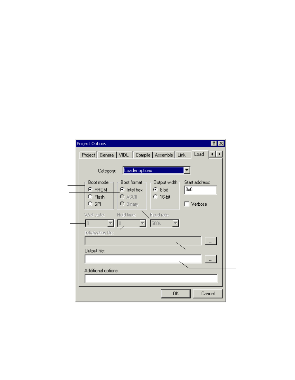
Blackfin Processor Loader/Splitter
Using Base Loader
The Load page of the Project Options dialog consists of multiple panes
and is the same and for all Blackfin processors. When you open the Load
page, the default loader settings (Loader options) for the selected processor are already set. As an example, Figure 2-14 shows the ADSP-BF532
processor’s default Load settings for PROM booting. Command-line
switches equivalent to the dialog box options are also identified. Refer to
“Command-Line Switches” on page 2-42 for more information on the
switches.
-b
-f
-baudrate
-waits
-holdtime
Figure 2-14. Base Load Page: Loader File Options Pane
-p #
-width
-v
-init
-o
VisualDSP++ Loader Manual 2-47
for 16-Bit Processors
Page 78

Blackfin Processor Loader Guide
Using the page controls, you can select or modify the loader settings.
Table 2-10 describes each loader control and corresponding setting. When
you are satisfied with default settings, click OK to complete the loader
setup.
Table 2-10. Base Loader Page Settings
Setting Description
Category Selections in the drop-down box display panes of options. The options are:
• Loader options – default booting options (this section)
• Boot kernel options – specification for a second-stage loader (see
on page 2-49)
• ROM splitter options – specification for the no-boot mode (see
on page 2-51)
If you do not use the boot kernel for ADSP-BF535 processors, the second Load
pane appears with all kernel option fields grayed out. The loader does not search
for the boot kernel if you boot from the on-chip ROM by setting the
-no2kernel command-line switch as described on page 2-45.
For ADSP-BF531/BF532/BF533 and ADSP-BF561 processors, which do not
have software boot kernels by default, you need to select the boot kernel to use
one.
Boot mode Specifies PROM, Flash, or SPI as a boot source.
Boot format Specifies Intel hex, ASCII, or binary formats.
Output width Specifies 8 or 16 bits.
If BMODE = 01 or 001 and Flash/PROM is 16-bit wide, the 16-bit option must
be selected.
Start address
Verbose Generates status information as the loader processes the files.
Wa it state Specifies the number of the wait states for external access ( 0–15).
Hold time Specifies the number of the hold-time cycles for PROM/Flash boot (0–3).
Specifies a PROM/Flash output start address in hex format for the application
code.
The selection is active for ADSP-BF535 processors. For ADSP-BF531,
ADSP-BF532, and ADSP-BF533 processors, the field is grayed out.
The selection is active for ADSP-BF535 processors. For ADSP-BF531,
ADSP-BF532, and ADSP-BF533 processors, the field is grayed out.
2-48 VisualDSP++ Loader Manual
for 16-Bit Processors
Page 79

Blackfin Processor Loader/Splitter
Table 2-10. Base Loader Page Settings (Cont’d)
Setting Description
Baud rate Specifies a baud rate for SPI booting (500 kHz, 1 MHz, and 2 MHz).
The selection is active for ADSP-BF535 processors. For ADSP-BF531,
ADSP-BF532, and ADSP-BF533 processors, the field is grayed out.
Initialization
file
Kernel file Specifies the boot kernel file. Can be used to override the default boot kernel if
Output file Names the loader’s output file.
Additional
options
Directs the loader to include the initialization file (Init code). The Initialization
file selection is active for ADSP-BF531/BF532/BF533, and ADSP-BF561 pro-
cessors. For ADSP-BF535 processors, the field is grayed out.
there is one by default, as on ADSP-BF535 processors.
Specifies additional loader switches. You can specify additional input files for a
multiinput system.
Note: The loader processes the input files in order the files appear on the command line, starting with the one from the project.
Using Second-Stage Loader
If you to use a second-stage loader, select Boot kernel options in the Category drop-down menu. The page shows how to configure the loader for
boot loading and to output file generation using the boot kernel.
Figure 2-15 shows an example boot kernel Load pane for a Blackfin
processor.
To create a loader file which includes a second-stage loader:
1. Use the Loader options pane to set up base booting options (see
“Using Base Loader” on page 2-47).
2. Select Boot kernel options from the Category drop-down box to
open the second Load pane with the second-stage loader settings,
shown in Figure 2-15.
VisualDSP++ Loader Manual 2-49
for 16-Bit Processors
Page 80

Blackfin Processor Loader Guide
-o2
-kb
-kf
-kp #
-kwidth
-l filename
Figure 2-15. ADSP-BF53x Processors: Boot Kernel Pane
3. Select Use boot kernel. By default, this option is selected for
ADSP-BF535 and grayed out for ADSP-BF531/BF532/BF533 and
ADSP-BF561 processors.
4. If you want to produce two output files (boot kernel file and application code file), select the Output kernel in separate file check
box. This option boots the second-stage loader from one source
and the application code from another source. If the Output kernel
in separate file box is selected, you can specify the kernel output
file options such as the Boot mode (source), Boot format, and
Output width.
2-50 VisualDSP++ Loader Manual
for 16-Bit Processors
Page 81

Blackfin Processor Loader/Splitter
5. Enter the Kernel file (.DXE). You must either use the default kernel
(in case of a ADSP-BF535 processor) or enter a kernel filename if
Use boot kernel in step 3 is selected.
The following second-stage loaders are currently available for the
ADSP-BF535 processor.
Boot Source Second Stage Loader File (or Boot Kernel File)
8-bit Flash/PROM 535_prom8.dxe,
16-bit Flash/PROM 535_prom16.dxe
SPI 535_spi.dxe
!
For ADSP-BF531, ADSP-BF532, ADSP-BF533, and
ADSP-BF561 processors, no second-stage loaders are required;
hence, no default kernel files are provided. Users can supply their
own second-stage loader file, if so desired.
6. Specify the Start address (FLash/PROM output address in hexadecimal format) for the kernel code. This option allows you to
place the kernel file at a specific location within the Flash/PROM
in the loader file.
7. For ADSP-BF535 processors only, modify the Wait states and
Hold time cycles for Flash/PROM booting or the Baud rate for
SPI booting.
8. Click OK to complete the loader setup.
Using ROM Splitter
Unlike the loader utility, the splitter does not format the application data
when transforming an
Whether data and/or instruction segment are processed by the loader or
.DXE file to an .LDR file. It emits raw data only.
VisualDSP++ Loader Manual 2-51
for 16-Bit Processors
Page 82

Blackfin Processor Loader Guide
splitter utility is controlled by the LDF’s TYPE() command. Segments
declared with TYPE(RAM) are consumed by the loader utility, and segments
declared by TYPE(ROM) are consumed by the splitter.
Figure 2-16 shows an example ROM splitter options pane of the Load
page. With the Enable ROM splitter box unchecked, only TYPE(RAM) seg-
ments are processed and all TYPE(ROM) segments are ignored by the
elfloader utility. If the box is checked, TYPE(RAM) segments are ignored
and TYPE(ROM) segments are processed by the splitter utility.
-romsplitter
-b
-width
-maskaddr #
-o
Figure 2-16. ROM Splitter Pane
The Mask Address field masks all EPROM address bits above or equal to
the number specified. For example, Mask Address =
the bits above and including
A29 (ANDed by 0x1FFF FFFF). Thus,
29 (default) masks all
2-52 VisualDSP++ Loader Manual
for 16-Bit Processors
Page 83

Blackfin Processor Loader/Splitter
0x2000 0000 becomes 0x0000 0000. The valid numbers are integers 0
through 32 but, based on your specific input file, the value can be within a
subset of [0, 32].
No-boot Mode
The hardware settings of BMODE = 000 for ADSP-BF535 processors or
BMODE = 00 for ADSP-BF531, ADSP-BF532, and ADSP-BF533 proces-
sors select the no-boot option. In this mode of operation, the on-chip
boot kernel is bypassed after reset and the processor starts fetching and
executing instructions from address 0x2000 0000 in the Asynchronous
Memory Bank 0. The processor assumes 16-bit memory with valid
instructions at that location.
To create a proper .LDR file that can be burned into either a parallel Flash
or EPROM device, you must modify the standard LDF file in order the
reset vector is to be located accordingly. The following code fragments
illustrate the required modifications in case of an ADSP-BF533 processor.
Listing 2-3. Section Assignment (LDF File)
MEMORY
{
/* Off-chip Instruction ROM in Async Bank 0 */
MEM_PROGRAM_ROM { TYPE(ROM) START(0x20000000) END(0x2009FFFF)
WIDTH(8) }
/* Off-chip constant data in Async Bank 0 */
MEM_DATA_ROM { TYPE(ROM) START(0x200A0000) END(0x200FFFFF)
WIDTH(8) }
/* On-chip SRAM data, is not booted automatically */
MEM_DATA_RAM { TYPE(RAM) START(0xFF903000) END(0xFF907FFF)
WIDTH(8) }
VisualDSP++ Loader Manual 2-53
for 16-Bit Processors
Page 84

Blackfin Processor Loader Guide
Listing 2-4. ROM Segment Definitions (LDF File)
PROCESSOR p0
{
OUTPUT( $COMMAND_LINE_OUTPUT_FILE )
SECTIONS
{
program_rom
{
INPUT_SECTION_ALIGN(4)
INPUT_SECTIONS( $OBJECTS(rom_code) )
} >MEM_PROGRAM_ROM
data_rom
{
INPUT_SECTION_ALIGN(4)
INPUT_SECTIONS($OBJECTS(rom_data) )
} >MEM_DATA_ROM
data_sram
{
INPUT_SECTION_ALIGN(4)
INPUT_SECTIONS($OBJECTS(ram_data) )
} >MEM_DATA_RAM
With the LDF file modified this way, the source files can now take advantage of the newly introduced sections, as in Listing 2-5.
Listing 2-5. Section Handling (Source Files)
.SECTION rom_code;
_reset_vector: l0 = 0;
1 = 0;
l2 = 0;
l3 = 0;
/* continue with setup and application code */
2-54 VisualDSP++ Loader Manual
for 16-Bit Processors
Page 85

/* . . . */
.SECTION rom_data;
.VAR myconst x = 0xdeadbeef;
/* . . . */
.SECTION ram_data;
.VAR myvar y;
/* note that y cannot be initialized automatically */
Blackfin Processor Loader/Splitter
VisualDSP++ Loader Manual 2-55
for 16-Bit Processors
Page 86

Blackfin Processor Loader Guide
2-56 VisualDSP++ Loader Manual
for 16-Bit Processors
Page 87

3 ADSP-219X DSP
LOADER/SPLITTER
This chapter explains how the loader/splitter program (elfloader.exe) is
used to convert executable files (.DXE) into boot-loadable, no-bootable, or
combined output files for ADSP-219x DSPs.
“ADSP-219x loader/splitter” refers to the loader/splitter program
designed for ADSP-2191, ADSP-2195, ADSP-2196, ADSP-21990,
ADSP-21991, and ADSP-21992 DSPs. The ADSP-2192-12 loader is
described in Chapter 4, “ADSP-2192-12 DSP Loader” on page 4-1.
Refer to “Introduction” on page 1-1 for the loader overview; the introduc-
tory material applies to all processor families. Loader operations specific to
the listed above processors are detailed in the following sections.
• “ADSP-219x DSP Booting” on page 3-2
Provides general information on boot sequences, kernels, and
streams.
• “ADSP-219x DSP Loader Guide” on page 3-19
Provides reference information on the command-line interface.
VisualDSP++ Loader Manual 3-1
for 16-Bit Processors
Page 88

ADSP-219x DSP Booting
ADSP-219x DSP Booting
The ADSP-219x loader/splitter creates a boot stream, non-boot stream, or
combinational output. The program accepts one executable file (.DXE) as
input and generates one file (.LDR) as output.
Upon powerup, a ADSP-219x DSP can be booted from the EPROM,
UART, SPI, or Host port. Booting can also be initiated in software after
RESET. Refer to the Application Note EE-131 and your DSP’s data sheet or
Hardware Reference manual for more information on system configura-
tion, peripherals, registers, and operating modes.
You can run the loader/splitter program from a command-line or from
within the VisualDSP++ IDDE. When working within the VisualDSP++,
specify options via the Load page of the Project Options dialog box.
!
To ensure correct operation of the loader, familiarize yourself with:
Option setting on the Load page correspond to switches displayed
on the command line.
• “ADSP-219x DSP Boot Modes” on page 3-3
• “ADSP-219x DSP Boot Kernel” on page 3-4
• “ADSP-219x DSP Boot Streams” on page 3-4
• “Parallel EPROM Boot Streams” on page 3-4
• “Host Booting” on page 3-10
• “UART Booting” on page 3-11
• “Serial EPROM Booting” on page 3-12
• “No-booting” on page 3-12
3-2 VisualDSP++ Loader Manual
for 16-Bit Processors
Page 89

ADSP-219x DSP Loader/Splitter
ADSP-219x DSP Boot Modes
At powerup, after the reset, the processor transitions into a boot mode
sequence configured by the BMODE2–0 pins. The BMODE pins are dedicated
mode-control pins; the pin states are captured and placed in the Reset
Configuration register as BMODE0, BMODE1, and OPMODE (see Table 3-1). The
register is also known as the System Configuration Register (SYSCR) with
I/O address 0x0 0204.
Table 3-1. ADSP-219x DSP Operation Modes
BMODE1
Pin
0 0 0 No-boot mode. Run from external 16-bit memory at
0 1 0 Boot from EPROM.
1 0 0 Boot from Host.
1 1 0 Reserved.
0 0 1 No-boot mode. Run from external 8-bit memory at
0 1 1 Boot from UART.
1 0 1 Boot from SPI (up to 4K bits).
BMODE0
Pin
OPMODE
Pin
Description
logical address 0x10000. Bypass ROM.
logical address 0x10000. Bypass ROM.
The OPMODE pin has a dual role; it acts as a boot-mode select during RESET
and determines whether the DSP’s third SPORT functions as a SPORT or
an SPI. It is possible for an application to require
ently at runtime than at
RESET (that is, boot from an SPI but use SPORT2
OPMODE to operate differ-
during runtime). In this case, the boot kernel is responsible for setting
OPMODE accordingly at the end of the booting process. Therefore, software
can change
OPMODE anytime during runtime, as long as the corresponding
peripherals are disabled at that time.
VisualDSP++ Loader Manual 3-3
for 16-Bit Processors
Page 90

ADSP-219x DSP Booting
ADSP-219x DSP Boot Kernel
A loader boot kernel refers to the resident program stored in a
24-bit-wide, 1K portion of ROM space responsible for booting the DSP.
The starting address of the boot ROM is 0xFF 0000 to 0xFF 03FF, the first
location of page 256, in 1-wait-stated memory. A boot interrupt vectors to
address 0xFF 0000. When a ADSP-219x DSP comes out of a hardware
reset, program control jumps to 0xFF 0000, and execution of the boot
ROM code begins.
On ADSP-219x DSPs, the highest 16 locations in page 0 program memory and the highest 272 locations in page 0 data memory are reserved for
use by the ROM boot routines (for setting up DMA data structures and
for initializing registers, among other tasks). Ensure that the boot
sequence entry code or boot-loaded program are not allowed into this
space.
ADSP-219x DSP Boot Streams
The ADSP-219x ROM-resident loader is designed to parse and load a specific boot-stream format. When booting from an external 8- or 16-bit
EPROM, the boot stream consists of header and block fields.
The first header in the boot stream is a common word that applies to all
booting modes, except UART. This header field specifies whether the
stream is guarded by a
or cleared, based on the booting method and specific command-line
switches specified by the user.
checksum. Individual bits within this word are set
Parallel EPROM Boot Streams
When booting from an external 8- or 16-bit EPROM, the first 16-bit
header field contains information on the number of wait states and the
physical width (8- or 16-bit) of the EPROM. The first header is also
known as a global header or a control word.
3-4 VisualDSP++ Loader Manual
for 16-Bit Processors
Page 91

ADSP-219x DSP Loader/Splitter
This first header is followed by the regular boot stream, that is, a series of
headers and data blocks. Most headers are followed by corresponding
blocks of data, but some headers indicate regions of memory that need to
be “zero-filled” and are not followed by data blocks.
Block Headers
Each block header consists of four or six 16-bit words:
• The first word consists of a flag that indicates whether the following block of data is a 24-bit or 16-bit payload or zero-initialized
data. The flag uniquely identifies the last block that needs to be
transferred.
• The second word contains the lower 16 bits of the 24-bit start
address for data loading (destination). The first octet is the 8 LSBs,
followed by the next most significant bits (15–8), and so on.
• The third word contains the upper-most 8 bits of the 24-bit destination address, padded (suffixed) with one byte of zeros.
• The fourth word contains the payload’s word count. Similar to the
address, the first octet is the 8 LSBs, and the second octet is the 8
MSBs.
An extra word appears when a checksum function is used to verify booting
accuracy. This fifth word (also a 16-bit field) is the CRC-16 checksum for
the header, and the data block immediately follows it. The CRC
word is optional. Activate the
checksum by running the loader utility with
checksum
the -checksum command-line switch (on page 3-21).
The header is buffered with a dummy word of zeros to ease the EMI
addressing issue.
EPROM booting can be performed in an 8-bit or 16-bit scenario. This
information is controlled by the “-width #” switch and is finally embed-
ded in the boot stream. Unlike non-boot mode, bus width is not
VisualDSP++ Loader Manual 3-5
for 16-Bit Processors
Page 92

ADSP-219x DSP Booting
controlled by the mode pins. The width information configures the EMI
interface and remains valid during the entire boot process. If you want to
boot off-chip memories, be aware that the width of the memory you want
to boot must be identical to the width of the interface from which you are
booting.
Data Blocks
The header is followed by the data block (also called payload data). The
16-bit block is sent in a 16-bit field, and the 24-bit block is sent in a
32-bit field.
!
When booting from an 8- or 16-bit EPROM, direct DSP core accesses
and Memory DMA (under the control of an EPROM boot routine located
in the ROM space) are used to load a boot-stream formatted program
located in the boot space. Appropriate packing modes are selected, based
on the requirements of the boot stream.
Each page of boot space is 64K words long, and 16-bits can address the
EPROM per page. The upper 8 address bits specify the boot page. Upon
hardware reset, booting is from address 0x0000 of logical page 0x80, which
mirrors physical address
available off-chip.
The External Port Interface (EPI) uses its default configuration
(divide-by-128 clock and 7 wait states) to access the EPROM. While
booting via EPROM boot space, the highest 16 locations in page 0 program memory block (0x7FF0 to 0x7FFF) and the top 272 locations of page
0 data memory block (
boot routines.
24-bit data block is represented differently in the boot stream from
24-bit addresses. 32-bit data block is transmitted the following
way—a byte of zeros (inserted by the loader), bits 0-7, followed by
bits 8-15, and finally bits 16-24.
0x000000 because the upper address lines are not
0xFEF0 to 0xFFFF) are reserved for use by the ROM
3-6 VisualDSP++ Loader Manual
for 16-Bit Processors
Page 93

ADSP-219x DSP Loader/Splitter
ADSP-219x DSP Multiple .DXE Support
VisualDSP++ 3.5 introduces support for multiple .DXE booting in Parallel
EPROM booting mode. Boot streams of multiple projects or applications
can be stored in a single EPROM. The on-chip boot kernel always boots
in application number 0. Its boot stream starts at EPROM address
0x000000. User-defined second-stage loaders or boot management soft-
ware may boot any application depending on application-specific
circumstances. Alternatively, one application can be loaded and executed
after the other terminates. The loader/splitter utility can consume multiple .DXE files and arrange their boot streams in several manners.
Use the following syntax to submit two or more executable files to the
loader:
elfloader File1.dxe [outputfile] -proc processor [-switch
...
]
[-pd addr [switches_specific_to_dxe_file_that_follows]] File2.dxe
[-pd addr [switches_specific_to_dxe_file_that_follows]] File3.dxe
File1.dxe is the default application that is booted by the on-chip boot
kernel after reset. Unless the -p switch is specified, the boot stream of
File1.dxe starts at EPROM address 0x000000.
If there is a –pd addr switch specified for an executable file (File.dxe), the
switches between “–pd” and “File.dxe” are called a pd grouping. The
addr” parameter is the address in the byte-based PROM address space.
“
The address should be a hex value. If –pd addr is absent from a command
line, no pd grouping is associated with the executable file, but the address
in the byte-based PROM address space remains associated with the
.DXE.
Usually the –pd addr switch is applied if the individual boot streams need
to be located a given addresses. For example, when the individual boot
streams need to reside is certain pages of a Flash memory device. If the different boot streams are going to reside in different physical PROM
devices, this syntax enables the user to assign different settings, such as
wait-states or even output file name to the individual
.DXEs.
...
VisualDSP++ Loader Manual 3-7
for 16-Bit Processors
Page 94

ADSP-219x DSP Booting
If more than one .DXE file is listed at the command line without -pd
switch, the loader utility appends the boot stream of the second .DXE
immediately to the one of the first .DXE and so on. Executable files inherit
boot stream settings from previous one if not explicitly set by a -pd
grouping.
The pd. grouping enables various options for the loader stream of the
input .DXE file. In the multiinput .DXE scenario, the loader stream for each
executable is same as when there is only one input executable supplied to
elfloader, with an exception of:
1. An artificial loader block (with header and data block) is created
right after the first (global) 16-bit header and before the regular
boot stream. The destination address in the header is same as that
of the first loader block in the regular boot stream. This means that
any data booted by the artificial loader block is to be overwritten
by the real data from the regular boot stream.
The content of this block’s payload is the pd value for the next
.DXE. If no pd grouping is specified for the next .DXE, the pd value
for the next .DXE is calculated by adding the pd value of the current
.DXE and the size (in bytes) of the current .DXE loader stream. If
there are no other .DXEs in the stream, the default value is zero.
You can overwrite the default by the –pdAddrNext switch.
The artificial loader block can be removed by turning on the
-noDxeAddrHdr command-line option.
2. The loader stream version, which is 4 bits in the first 16-bit header.
Note that both of these modifications are backward compatible with the
ADSP-2191 boot kernel. The optional
[
switches_specific_to_dxe_file_that_follows] may include:
Example
3-8 VisualDSP++ Loader Manual
for 16-Bit Processors
Page 95

ADSP-219x DSP Loader/Splitter
-o Output file (.LDR) for the current and following .DXEs (see “-o filename” on
page 3-22).
-opmode Opmode for the current and following .DXEs (see “-opmode #” on page 3-22).
-p The Intel hex offset for th e current loader file (see “-p address” on page 3-22).
-width Width for the current and following .DXEs (see “-width #” on page 3-24).
-wait The number of wait states for this and following .DXEs (see “-waits #” on
page 3-24).
-clkdivide Clkdivide for this and following .DXEs (see “-clkdivide #” on page 3-21).
-maskaddr Address bits to be masked off for this and following .DXEs (see “-maskaddr #” on
page 3-22).
There are four executable files (streams):
• Application 1 (app1.dxe) starts at byte address 0x000000 (ROM)
• Application 2 (app2.dxe) appends to Application 1 (ROM)
• Application 3 (app3.dxe) starts at 0x020000 (flash page 1)
• Application 4 (app4.dxe) starts at 0x030000 (flash page 2)
The task is to create two loader files, one is 16-bit ROM from 0x000000 to
0x01FFFF and one is 8-bit Flash from 0x020000 to 0x03FFFF.
There are two different ways to accomplish the task:
1. Use VisualDSP++ Flash Programmer plug-in to burn the Flash. In
this scenario, the real byte address is expected:
elfloader -proc ADSP-2191 -b PROM -width 16 app1.dxe
app2.dxe -pd 0x20000 -p 0x20000 -width8 -o flash.ldr
app3.dxe -pd 0x30000 app4.dxe
Since the -p value is reset to a zero whenever an -o is specified, the
!
addresses in the Intel hex record starts at zero for
flash.ldr.
2. Equivalently, invoke the loader twice:
VisualDSP++ Loader Manual 3-9
for 16-Bit Processors
Page 96

ADSP-219x DSP Booting
elfloader -proc ADSP-2191 -b PROM -width 16 app1.dxe
app2.dxe -pdAddrNext 0x20000
elfloader -proc ADSP-2191 -b PROM -width 8 -o flash.ldr -pd
0x20000 -p 0x20000 app3.dxe -pd 0x30000 app4.dxe
!
you may specify -pEqualPD:
elfloader -proc ADSP-2191 -b PROM -width 16 app1.dxe
app2.dxe -pd 0x20000 -pEqualPD -width8 -o flash.ldr
app3.dxe -pd 0x30000 app4.dxe
With the -NoDxeAddrHdr switch, this artificial block is not inserted. Then
the user loader can still parse the complete boot stream, block by block
until it detects a final-init block. Since the default -p value is reset to a
zero whenever an -o is specified, the addresses in the Intel hex record has
to be explicitly set to 0x20000 for flash.ldr.
It is very likely that second-stage loaders and similar type of programs execute directly from the EPROM. Thus, this multiple .DXE scenarios are
often combined with the features discussed in “Enriching Boot EPROMs
with No-boot Data” on page 3-16.
Host Booting
Host booting is performed in either an 8-bit or 16-bit scenario. By
default, little-endian format is used. If configured in Host boot mode, the
DSP does not support the boot process actively. It is the host’s responsibility to initialize the DSP memories properly. The DSP passively waits
until the host writes a “1” to the Semaphore A register (IO address
0x1CFC). Then the DSP starts fetching and executing instructions at
In cases where the -pd and -p values are expected to be the same,
address
0x00 0000.
3-10 VisualDSP++ Loader Manual
for 16-Bit Processors
Page 97

ADSP-219x DSP Loader/Splitter
It is recommended that the host parses the boot stream and downloads
segment by segment. The elfloader.exe may store the boot stream as an
Intel hex-32 file typically required by embedded host devices. PC-based
hosts may favor the ASCII format, which stores one byte or one 16-bit
word per line.
UART Booting
When booting via the UART port, a host downloads a boot stream formatted program to the DSP following an auto-baud handshake sequence.
The auto-baud feature simplifies system design because you do not need
to calculate boot clock rates as a function of crystal frequency, core clock
divider, peripheral clock mode, and so on.
The booting host can select a baud rate (including a non-standard rate)
anywhere within the UART clocking capabilities.
Following a hardware or software reset, the ADSP-219x DSP monitors the
UART transceiver channel and expects the predefined character (0xAA) to
determine the bit rate. The DSP replies an “OK” string to acknowledge the
bit rate.
Afterwards, the host may send the complete boot stream (8 data bits, no
parity, 1 stop bit) without further handshake. The boot stream is decoded
by the DSP and starts program execution automatically.
!
This boot operation is controlled by a UART boot routine in the internal
ROM space. While booting via UART, the highest 16 locations in page 0
program memory block (0x7FF0 to 0x7FFF) and the top 272 locations of
page 0 data memory block (
ROM boot routine.
VisualDSP++ Loader Manual 3-11
for 16-Bit Processors
Compared to other formats, the ADSP-2191/2195/2196 UART
boot stream suppresses the very first byte. To force the loader utility to include the first byte, use the
(on page 3-21).
0xFEF0 to 0xFFFF) are reserved for use by the
-forcefirstbyte switch
Page 98

ADSP-219x DSP Booting
Serial EPROM Booting
The SPI0 port is used when booting from an SPI-compatible EPROM.
The SPI port selects a single serial EPROM device using the PF0 pin as a
chip select, submits a read command and address 0x00, and begins to
clock consecutive data into memory (internal memory or external memory) at a SCK clock frequency of HCLK/60. The DSP streams the
complete boot image in and processes it without further handshake with
the SPI EPROM.
Two types of SPI EEPROM devices are supported: devices of 4K bytes
and smaller (12-bit address range), and those larger than 4K bytes (16-bit
address range). The SPI boot stream may not exceed 64 kilobytes.
This boot operation is controlled by an SPI boot routine in internal ROM
space. While booting via serial EPROM, the highest 16 locations in
page 0 program memory block (0x7FF0 to 0x7FFF) and the top 272 locations of page 0 data memory block (0xFEF0 to 0xFFFF) are reserved for use
by the ROM boot routine. Refer to the Application Note EE-145 for SPI
booting examples.
No-booting
When BMODE2-0 is strapped to a 000 or 001, the ADSP-219x DSP comes
out of hardware reset and begins to execute code from page 1 memory
space (
the BMODE0 pin (0 = 8-bit ext/24-bit int, 1 = 16-bit ext/24-bit int). By
default, the External Port Interface (EPI) is configured to operate with the
divide-by-128 clock and a read wait-state count of 7.
0x01 0000). The specified packing mode depends on the state of
No-boot mode does not use boot-stream format.
!
After reset, the DSP starts program execution from external address
0x010000. When the no-boot option is selected, the DSP typically expects
an 8- or 16-bit EPROM or Flash device connected to the memory strobe
3-12 VisualDSP++ Loader Manual
for 16-Bit Processors
Page 99

ADSP-219x DSP Loader/Splitter
signal (/MS0). Splitter capabilities of the ADSP-219x loader utility support
the generation of the required EPROM image files. Refer to the loader’s
-romsplitter switch (see on page 3-23) for more information.
Non-bootable memory segments are declared by the TYPE(ROM) command
in the Linker Description File (.LDF). The WIDTH() command specifies the
physical EPROM width (which equals to the EMI port setting). Every
.LDF file that belongs to a no-boot project should define a proper memory
segment; as in the following example,
MEMORY {
...
seg_ext_code {
TYPE(PM ROM) START(0x010000) END(0x017FFF) WIDTH(16) }
...
}
The START(), END(), and LENGTH() commands expect logical addresses.
Since the example segment stores 24-bit-wide instructions, the TYPE(PM)
command defines the logical width of the segment to be 24-bits. The
example assumes no-boot mode (000) and runs from external memory
starting at address 0x010000. This is why the WIDTH(16) command sets the
physical width to 16 bits. Due to ADSP-219x EMI packing rules, the first
instruction is stored in the physical 16-bit EPROM location 0x020000.
The 16-bit EPROM address locations between 0x010000 and 0x01FFFF
can be used by an additional read-only data segment as shown below.
MEMORY {
...
seg_ext_code {
TYPE(PM ROM) START(0x010000) END(0x017FFF) WIDTH(16) }
seg_ext_data {
TYPE(DM ROM) START(0x010000) END(0x01FFFF) WIDTH(16) }
...
}
VisualDSP++ Loader Manual 3-13
for 16-Bit Processors
Page 100

ADSP-219x DSP Booting
The data segment seg_ext_data is defined by the TYPE(DM) command,
which sets the logical width to 16 bits. Since the WIDTH(16) command also
sets the physical width to 16 bit, no data packing and no address multiply
is required. Logical addresses are equal to physical EPROM addresses in
this special case. The 16-bit EPROM image generated by the loader is
described in Table 3-2:
Table 3-2. EPROM Image Description
Address range Purpose
0x000000–0x00FFFF
0x010000–0x01FFFF
0x020000–0x02FFFF seg_ext_code
Not used
seg_ext_data
The DSP cannot access off-chip addresses lower than 0x010000.
!
Typically this address space is accessed by taking advantage of
address aliasing. The memory strobe (/MS0) covers an address range
from 0x010000 to 0x400000. For example, if the EPROM size is less
than 4M words and the EPROM is the only device connected to
/MS0, the first 64K words can be accessed through addresses
0x200000 to 0x20FFFF.
If a project consists only of two segments (seg_ext_data and
seg_ext_code), a 128K x 16-bit EPROM device would be sufficient to
store all the required data and instructions. If the loader utility is invoked
with the -maskaddr 17 switch (on page 3-22), all physical address bits
greater than or equal to A17 are masked out. The loader ANDs all physical
addresses with 0x01FFFF. The resulting EPROM image maps segment
seg_ext_code into the unused space below 0x010000 (see Table 3-3).
This way, a 128K x 16-bit EPROM can be burned properly. At runtime,
seg_ext_code aliases back to the addresses above 0x020000 when address
lines
A17 through A21 are not connected.
3-14 VisualDSP++ Loader Manual
for 16-Bit Processors
 Loading...