ANALOG DEVICES UG-112 Service Manual

Evaluation Board User Guide
NOTES
1. THE EVALUATION BOARD SIL KS CRE E N P ART
NUMBER LABELLING ON YOUR BOARD MAY
BE DIFFE RE NT FROM WHAT IS S HOWN HERE.
08951-001
NOTES
1. THE EVALUATION BOARD SIL KS CRE E N P ART
NUMBER LABELLING ON YOUR BOARD MAY
BE DIFFE RE NT FROM WHAT IS S HOWN HERE.
08951-002
UG-112
One Technology Way • P. O. Box 9106 • Norwood, MA 02062-9106, U.S.A. • Tel: 781.329.4700 • Fax: 781.461.3113 • www.analog.com
Evaluation Board for Single, High Speed Op Amps
Offered in 5-Lead SC-70 Packages
FEATURES
Enables quick breadboarding/prototyping
User-defined circuit configuration
Edge-mounted SMA connector provisions
Easy connection to test equipment and other circuits
RoHS compliant
GENERAL DESCRIPTION
The Analog Devices, Inc., SC-70 evaluation board is designed to
help users evaluate single, high speed op amps offered in 5-lead
SC-70 packages. The evaluation board is a bare board (that is,
there are no components or amplifier soldered to the board,
these must be ordered separately) that enables users to quickly
prototype a variety of single op amp circuits, which minimizes
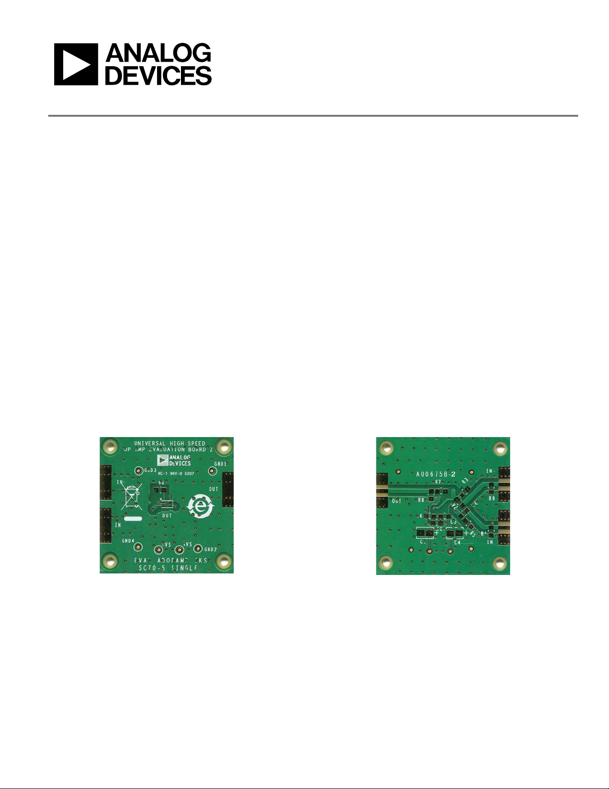
risk and reduces time to market. Figure 1 shows the component
side of the bare evaluation board, and Figure 2 shows the circuit
side of the bare evaluation board.
EVALUATION BOARD COMPONENT AND CIRCUIT SIDES
The 2-layer evaluation board accepts SMA edge-mounted connectors on the inputs and outputs for efficient connection to test
equipment or other circuitry. The ground plane, component
placement, and supply bypassing are designed to minimize
parasitic inductance and capacitance. The evaluation board
components are primarily SMT 1206 case size, with the
exception of the electrolytic bypass capacitors (C1 and C4),
which are 3528 case size.
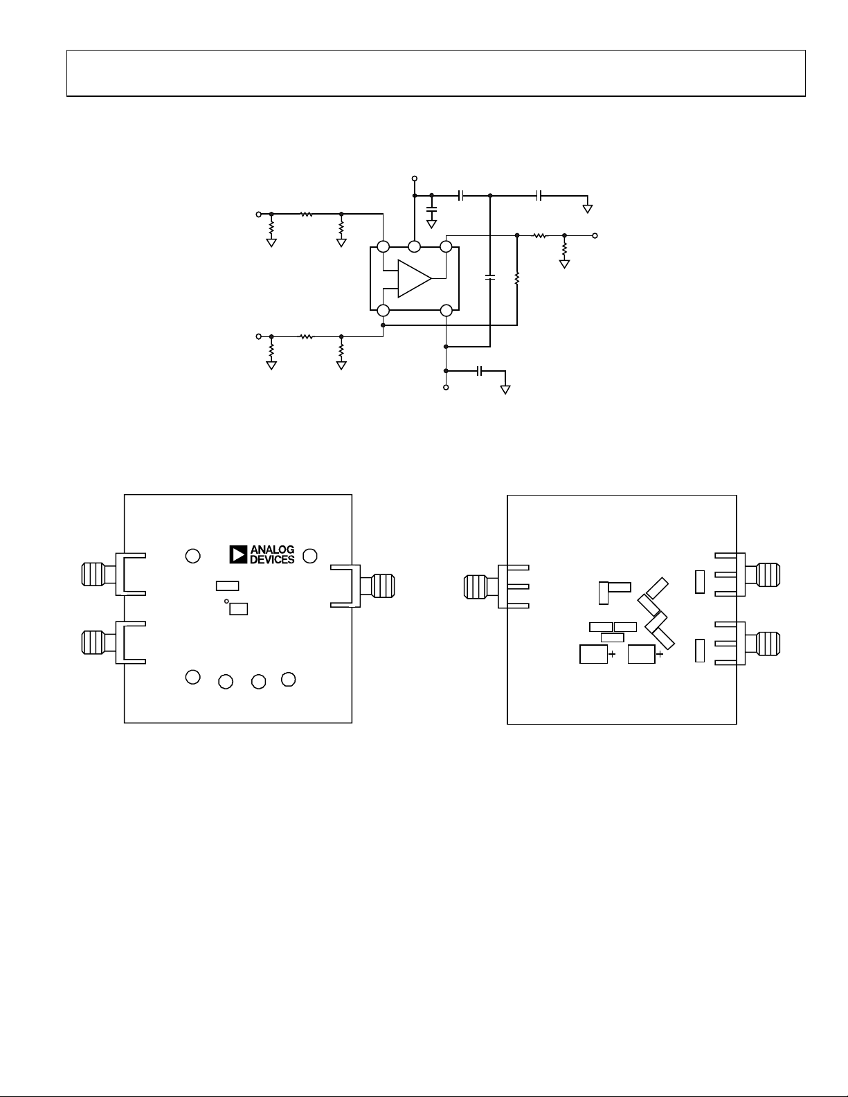
Figure 3 shows the evaluation board schematic. The PCB
assembly drawings are shown in Figure 4 and Figure 5. The
layout pattern for the PCB is shown in Figure 6 and Figure 7.
Figure 1. Component Side of Evaluation Board
PLEASE SEE THE LAST PAGE FOR AN IMPORTANT
WARNING AND LEGAL TERMS AND CONDITIONS.
Figure 2. Circuit Side of Evaluation Board
Rev. A | Page 1 of 8

UG-112 Evaluation Board User Guide
TABLE OF CONTENTS
Features .............................................................................................. 1
General Description ......................................................................... 1
Evaluation Board Component and Circuit Sides ......................... 1
Revision History ............................................................................... 2
REVISION HISTORY
4/11—Rev. 0 to Rev. A
Changes to User Guide Title and General Description Section . 1
Changes to Figure 3 Captions ......................................................... 3
4/10—Revision 0: Initial Version
Evaluation Board Schematic, Assembly Drawings, and Layout
Patterns ...............................................................................................3
Ordering Information .......................................................................5
Bill of Materials ..............................................................................5
Rev. A | Page 2 of 8

Evaluation Board User Guide UG-112
R4*
R1* R5*
R2*
R9* R3*
R8*
R7*
R6*
C2*
SC70
–
+
C4
C5* C6*
10µF
C1
10µF
+IN
3
4 5
2 1
–VS
–IN
+VS
OUT
+
+
*USER-DEFI NE D V ALUE
08951-003
*SMA EDGE CO NNE CTOR JOHNSON COMPO NE NTS, INC. P/N 142-0701- 831
*
*
*
UNIVERSAL HIGH SPEED
OP AMP EVALUATION BOARD Z
OUT1
GND1GND3
GND4
GND2
–VS +VS
IN–
OUT
IN+
R6
DUT
EVAL-ADOPAMP-1KS
SC7O-5 SINGLE
08951-004
A00675B
R7
R8
R3
R2
R4
R5
R1
R9
IN–
IN+
OUT
C6
C1
C2
C4
C5
08951-005
EVALUATION BOARD SCHEMATIC, ASSEMBLY DRAWINGS, AND LAYOUT PATTERNS
Figure 3. Evaluation Board Schematic
Figure 4. Component Side Assembly Drawing
Figure 5. Circuit Side Assembly Drawing
Rev. A | Page 3 of 8
 Loading...