Evaluation Board User Guide
One Technology Way • P. O . Box 9106 • Norwood, MA 02062-9106, U.S.A. • Tel : 781.329.4700 • Fax : 781.461.3113 • www.analog.com
UG-071
Setting Up the Evaluation Board for the ADCLK846
PACKAGE LIST
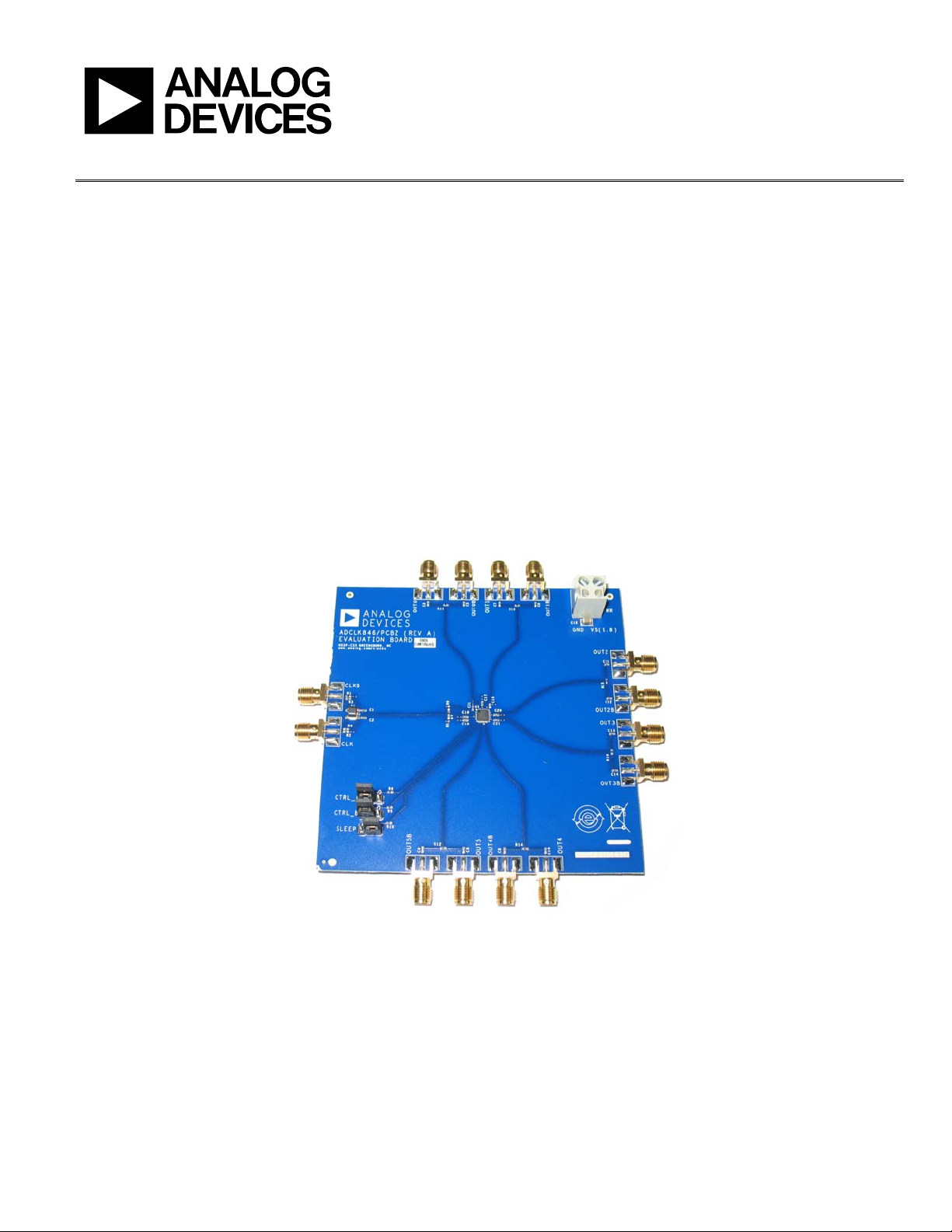
Evaluation board with components installed
Applicable documents (schematic and layout)
GENERAL DESCRIPTION
This user guide describes how to set up and use the evaluation
board for ADCLK846. The ADCLK846 data sheet contains full
technical details about the specifications and operation of this
device and should be consulted when using the evaluation board.
The ADCLK846 is a high performance clock fanout buffer.
The evaluation board is fabricated using a high quality Rogers®
dielectric material. Transmission line paths are kept as close to
100 Ω differentially as possible.
Figure 1. Evaluation Board
Please see the last page for an important warning and disclaimers. Rev. 0 | Page 1 of 8
08670-001

UG-071 Evaluation Board User Guide
TABLE OF CONTENTS
Package List ....................................................................................... 1
General Description ......................................................................... 1
Revision History ............................................................................... 2
Recommended Board Setup ............................................................ 3
REVISION HISTORY
12/09—Revision 0: Initial Version
Clock Outputs ................................................................................4
Evaluation Board Schematics and Artwork ...................................5
ESD Caution...................................................................................8
Rev. 0 | Page 2 of 8

Evaluation Board User Guide UG-071
RECOMMENDED BOARD SETUP
The recommended setup for the ADCLK846 evaluation board
is shown in Figure 2. V
is set to 1.8 V.
S
The CLK input is set up for single-ended-to-differential
operation via the balun on the evaluation board. In addition,
series capacitors (C3 and C4) in the path provide ac-coupled
inputs to the ADCLK846.
POWER SUPPLY
1.8V GND
The range of the peak-to-peak input voltage swing at CLK is
0.15 V to 1.8 V. Output jitter performance is degraded by input
slew rate, as shown in the ADCLK846 data sheet.
Table 1. Basic Equipment Required
Quantity Description
1 Single power supply
1 Signal source
1 High bandwidth oscilloscope
1 High bandwidth differential probe
2 Matched high speed cables
BOARD
GND
OUTx
OUTx
PROBE
OSCILLOSCOPE
08670-002
CLOCK
SOURCE
V
S
CLK
CLK
Figure 2. Recommended Setup for ADCLK846 Evaluation
ADCLK846
EVALUATION
Rev. 0 | Page 3 of 8
 Loading...