Evaluation Board User Guide
One Technology Way • P.O . Box 9106 • Norwood, MA 02062-9106, U.S.A. • Tel : 781.329.4700 • Fax : 781.461.3113 • www.analog.com
UG-063
Evaluating the ADM1062 to ADM1169 for Complex Sequencing
FEATURES
Full-featured evaluation kits for ADM1062 to ADM1169
I²C interface supports all product-related software
10 adjustable voltages reference for input emulation
Switch-controlled, open-drain/push-pull digital inputs
Extra headers for easy probing
Includes point to point patch cables for easy wiring
Multiboard cascade support
EVALUATION KIT CONTENTS
EVAL-ADM1062CASZ to EVAL-ADM1169CASZ
evaluation board
ADM1062 to ADM1169 device socket
8-way, 150 mm Micromatch ribbon cable
Patch cables
ADDITIONAL EQUIPMENT NEEDED
USB-to-I²C dongle USB-SMBUS-CABLEZ
9 V to 14.4 V power supply
RELATED DOCUMENTS
ADM1062 to ADM1169 data sheets
SOFTWARE NEEDED
ADM1062 to ADM1169 evaluation software
GENERAL DESCRIPTION
This user guide describes how to use the ADM1062 to
ADM1169 evaluation kits. The kits provide all of the support
circuitry required to operate the ADM1062/ADM1063/
ADM1064/ADM1065/ADM1066/ADM1067/ADM1068/
ADM1069/ADM1166/ADM1168/ADM1169 (hereafter referred
to as ADM1062 to ADM1169) in their various modes and
configurations, including multiple board setups. The ADM1062
to ADM1169 data sheets, available at www.analog.com, provide
additional information, and should be consulted when using the
evaluation board. All documents and software tools are
available at www.analog.com/power-management.
Note that USB-SMBUS-CABLEZ is not included in the
evaluation kit and should be ordered separately. Only one
dongle is required in multiboard cascade setup. One device
socket is included in each kit. Sockets for different device
packages are not included. Refer to the Socket Selection Guide
section for details regarding the corresponding socket types.
EVALUATION KIT SELECTION GUIDE
Table 1. Contents of Available Evaluation Kits
Evaluation Kit Model Contains Evaluation Board Contains IC Socket Corresponding Devices
EVAL-ADM1062TQEBZ EVAL-ADM1062-69CASZ SOCKET-ADM106xTQZ ADM1062ASUZ
EVAL-ADM1063TQEBZ EVAL-ADM1062-69CASZ SOCKET-ADM106xTQZ ADM1063ASUZ
EVAL-ADM1064TQEBZ EVAL-ADM1062-69CASZ SOCKET-ADM106xTQZ ADM1064ASUZ
EVAL-ADM1065TQEBZ EVAL-ADM1062-69CASZ SOCKET-ADM106xTQZ ADM1065ASUZ
EVAL-ADM1066TQEBZ EVAL-ADM1062-69CASZ SOCKET-ADM106xTQZ ADM1066ASUZ
EVAL-ADM1067TQEBZ EVAL-ADM1062-69CASZ SOCKET-ADM106xTQZ ADM1067ASUZ
EVAL-ADM1068LQEBZ EVAL-ADM1062-69CASZ SOCKET-ADM106xLQZ ADM1068ASTZ
EVAL-ADM1069LQEBZ EVAL-ADM1062-69CASZ SOCKET-ADM106xLQZ ADM1069ASTZ
EVAL-ADM1166TQEBZ EVAL-ADM1062-69CASZ SOCKET-ADM106xTQZ ADM1166ASUZ
EVAL-ADM1168LQEBZ EVAL-ADM1062-69CASZ SOCKET-ADM106xLQZ ADM1168ASTZ
EVAL-ADM1169LQEBZ EVAL-ADM1062-69CASZ SOCKET-ADM106xLQZ ADM1169ASTZ
PLEASE SEE THE LAST PAGE FOR AN IMPORTANT
WARNING AND LEGAL TERMS AND CONDITIONS.
Rev. A | Page 1 of 20

UG-063 Evaluation Board User Guide
TABLE OF CONTENTS
Features.............................................................................................. 1
Evaluation Kit Contents................................................................... 1
Additional Equipment Needed....................................................... 1
Related Documents ..........................................................................1
Software Needed............................................................................... 1
General Description ......................................................................... 1
Evaluation Kit Selection Guide....................................................... 1
Revision History ............................................................................... 2
Evaluation Board Hardware............................................................ 3
Supported Devices........................................................................ 3
Power Supplies ..............................................................................3
Inputs Emulation .......................................................................... 3
Output Signals............................................................................... 3
REVISION HISTORY
9/11—Rev. 0 to Rev. A
Changes to Package Contents Section, changes to General
Description Section, and Added Table 1 ....................................... 1
Changes to Output Signals Section and Changes to Figure 1 .... 3
Changes to Figure 2.......................................................................... 4
Changes to Table 2............................................................................ 5
Changes to Table 5............................................................................ 7
Added Evaluation Kits Quick Start Guide, added Figure 4 to
Figure 16, Renumbered Sequentially........................................... 10
2/10—Revision 0: Initial Version
IC Interface...................................................................................4
Multiple Board Setup....................................................................4
Switch, Jumper, and LED Functions...........................................5
Socket Selection Guide .................................................................8
Margining Guide ...............................................................................9
Evaluation Kit Quick Start Guide................................................. 10
Hardware Setup .......................................................................... 10
Software Setup ............................................................................ 11
Demo 1 ........................................................................................ 12
Demo 2 ........................................................................................ 13
Evaluation Board Schematics........................................................ 14
Ordering Information.................................................................... 18
Bill of Materials........................................................................... 18
Rev. A | Page 2 of 20

Evaluation Board User Guide UG-063
EVALUATION BOARD HARDWARE
The EVAL-ADM1062-69CASZ evaluation board is designed for
advanced evaluation of ADM1062 to ADM1169 SuperSequencer®
ICs. The board is easy to use, easy to probe, allows flexible
wiring, and offers multiple board cascadability.
SUPPORTED DEVICES
The evaluation board is designed to support all ADM1062
to ADM1169 devices in various packages. A device socket is
generally required for use with this board.
Devices can be easily fitted and changed using the ADM1062 to
ADM1169 device sockets. Solder pads for a single 48-lead thin,
plastic quad flat package (TQFP) is also available on the board,
allowing the user to solder parts onto the board.
Note the labeling on the board. For example, VP1/VX4 indicates a change in function depending on the ADM1062 to
ADM1169 device in use. The text on the left, VP1, is for use
with the ADM1062 to ADM1067 and ADM1166, whereas
the text on the right, VX4, is for use with the ADM1068/
ADM1069/ADM1168/ADM1169.
POWER SUPPLIES
The evaluation board can accept 9 V to 14.4 V from a bench
power supply through Connector J1 and Connector J2. It also
supports a wall-mountable switching power supply with the
same voltage range using Connector J3. J3 is grounded in the
core and has polarity protection circuits to prevent damage
due to incorrect polarity setup.
INPUTS EMULATION
Ten onboard adjustable voltage regulators from Analog Devices,
Inc., provide input supply emulation for all different setups
supported by the ADM1062 to ADM1169 devices. Each regulator operates independently and output voltages can be easily
adjusted by hand using an on-board rotating potentiometer.
Every regulator can be enabled or disabled by the user or by
the ADM1062 to ADM1169 device, depending on the jumper
configuration. Each regulator has an LED assigned to it to
indicate its status.
All regulators have a feedback pin that allows the user to evaluate
the margining function of the ADM1062 to ADM1169 devices.
An additional on-board two-way, push-pull/open-drain switch,
S3, can be used by the user to emulate digital inputs, if required.
OUTPUT SIGNALS
PDO output signals from the ADM1062 to ADM1169 devices
can be easily wired across to the regulator enable control
circuits to control the on-board voltage regulators. This allows
the board to perform simulations for real-world sequencing
applications. The DAC output signals can also be wired to the
feedback node of the regulators to achieve supply margining.
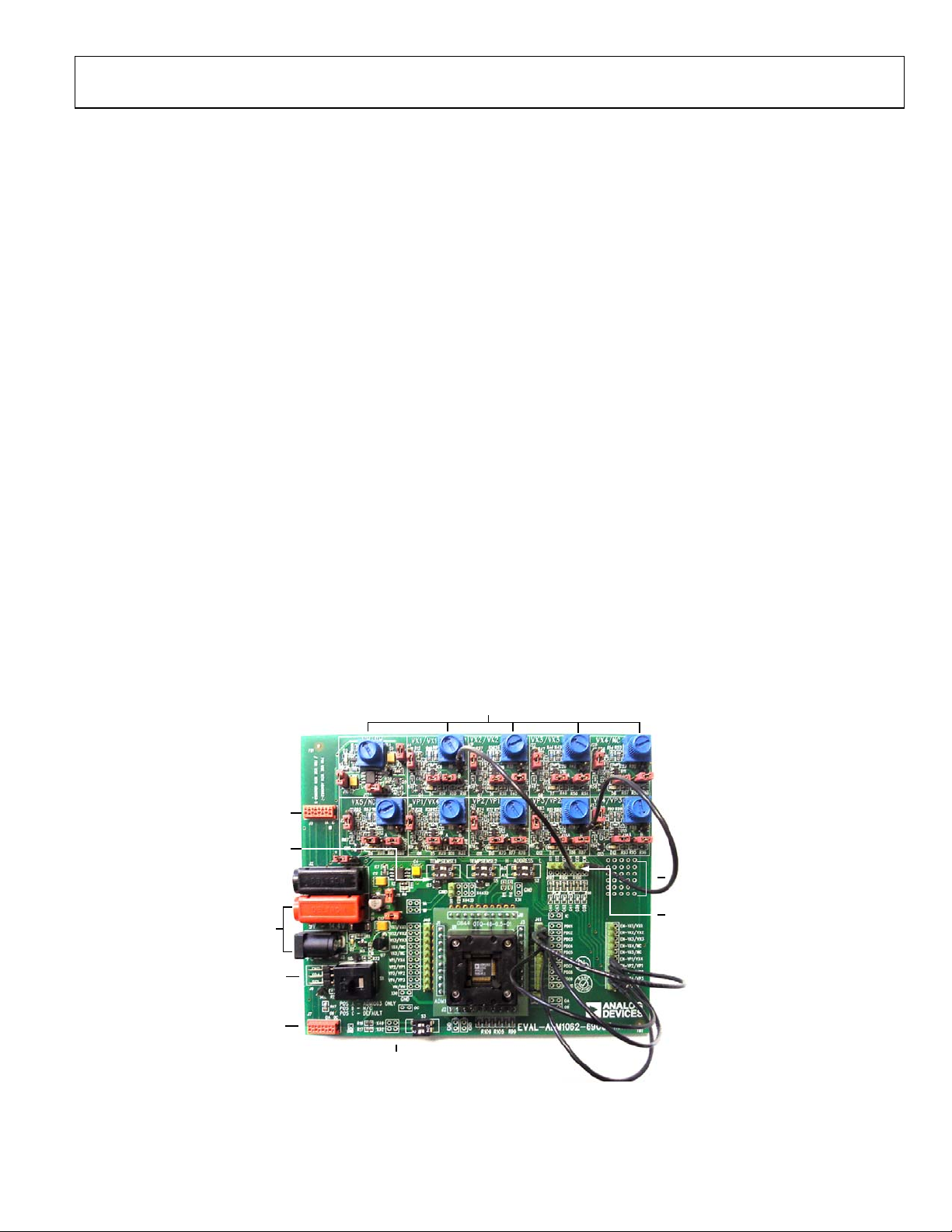
The wiring is made easy with the point-to-point patch cables
included in the evaluation kit. The user can easily cross link
the PDO output to a regulators enable input or connect DAC
outputs to a regulator’s feedback node.
MULTIBOARD
CONNECTOR
TEMPERATURE
SENSORS
POWER INPUT
9V TO 14.4V
2
I
C CONNECTOR
MULTIBOARD
CONNECTOR
ADJUSTABLE
REG
ULATORS
OPTIONAL
DIGIT AL I NP UT
Figure 1. Evaluation Board Wiring with Point-To-Point Patch Cables
DEVELOPMENT
AREA
DAC
MARGINING
OUTPUTS
08644-001
Rev. A | Page 3 of 20

UG-063 Evaluation Board User Guide
I²C INTERFACE
The evaluation board supports an IC interface. The user can
connect from the PC USB port to the board using the USBSMBUS-CABLEZ dongle from Analog Devices. The dongle has
internal pull-ups for the SDA and SCL bus. Users can use their
own IC cable. The evaluation board can provide on-board
3.3 V voltage pull-up by populating R21 and R22.
The board is compatible with all ADM1062 to ADM1169
evaluation software.
MULTIPLE BOARD SETUP
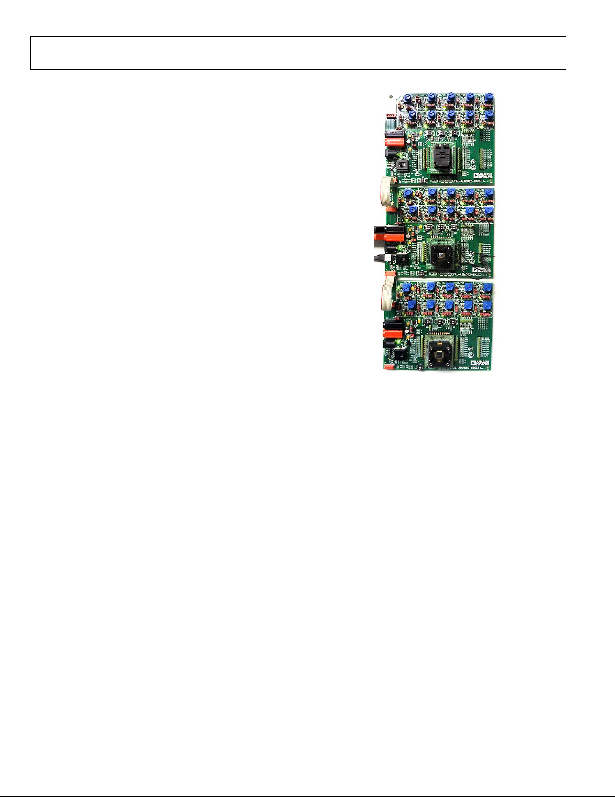
Connector J7 and Connector J9, along with the eight-way
ribbon cable, allow multiple EVAL-ADM1062-69CASZ boards
to be connected together to evaluate complex cascade sequencing setups.
The connection cable carries both power and IC communication signals across every board that is connected. The user only
needs to connect the power and IC cable to one board. It is
recommended to connect the power supply to the board in the
middle of the multiple board setup to avoid uneven power
dissipation in the traces/cables.
Apart from power and IC signals, the cable also links three
independent GPIO signal lines between the two boards that
it connects. The user can connect them to the inputs and/or
outputs of the ADM1062 to ADM1169 devices to achieve
sequencing across multiple boards. This allows multiple
ADM1062 to ADM1169 devices to work together to increase
the number of supply rails to be sequenced and monitored.
Figure 2. Multiple Boards Connection
08644-002
Rev. A | Page 4 of 20

Evaluation Board User Guide UG-063
SWITCH, JUMPER, AND LED FUNCTIONS
Table 2. Connector Functions
Switch Description Default
S1 I2C/mode control switch.
S1-A Position A allows the use of the ADM1063 device.
Position B allows the board to be isolated from I
Position C allows the use of the ADM1062, ADM1064 to ADM1069, ADM1166, ADM1168, and
ADM1169 devices.
S2 Device address switch.
S2-1 On: Address Pin A0 pulled down to ground.
Off: Address Pin A0 pulled up to VDDCAP.
S2-2 On: Address Pin A1 pulled down to ground.
Off: Address Pin A1 pulled up to VDDCAP.
S3 Optional digital input switch.
S3-1 Use in conjunction with X49.
X49 connected: push-pull. Disconnected
X49 disconnected: open-drain.
On: X49 pulled to ground. Off
Off: X49 pulled to 3.3 V/high impedance.
S3-2 Use in conjunction with X32.
X32 connected: push-pull. Disconnected
X32 disconnected: open-drain.
On: X32 pulled to ground. Off
Off: X32 pulled to 3.3 V/high impedance.
S4 External Temperature Sensor 1 control switch (for use with the ADM1062 and ADM1063).
S4-1, S4-2 Both on: External Temperature Sensor 1 connected.
Both off: External Temperature Sensor 1 disconnected.
S5 External Temperature Sensor 2 control switch (for use with the ADM1063 only).
S5-1, S5-2 Both on: External Temperature Sensor 2 connected.
Both off: External Temperature Sensor 2 disconnected.
2
C communications.
Position C
Off
Off
Both off
Both off
Table 3. Jumper Functions
Jumper Corresponding Regulator/Rails Description Default
J13 VH/VH
J6 VX1/VX1
J20 VX2/VX2
J23 VX3/VX3
J26 VX4/NC
J29 VX5/NC
J14 VP1/VX4
J32 VP2/VP1
J35 VP3/VP2
J38 VP4/VP3
J11 7 V (intermediate)
J12 3.3 V (pull-up)
Rail isolation jumper. Disconnect to isolate the
corresponding regulators from its power supply. Can be
used for debug.
Rev. A | Page 5 of 20
Connected

UG-063 Evaluation Board User Guide
Jumper Corresponding Regulator/Rails Description Default
J10 VH Controls the output of the VH regulator. Connected
J15
J17 VH/VH
J16 VX1/VX1
J21 VX2/VX2
J24 VX3/VX3
J27 VX4/NC
J30 VX5/NC
J18 VP1/VX4
J33 VP2/VP1
J36 VP3/VP2
J39 VP4/VP3
J4 VX1/VX1
J19 VX2/VX2
J22 VX3/VX3
J25 VX4/NC
J28 VX5/NC
J8 VP1/VX4
J31 VP2/VP1
J34 VP3/VP2
J37 VP4/VP3
J40 VXx/VPx/VH Connector used for device inputs probing.
J41 PDOx Connector used for device outputs probing.
ADM1062 to ADM1169 VH pin
Controls the source voltage connected to the VH pin of
the ADM1062 to ADM1169 device.
Connect left: connect VH pin to on-board VH regulator.
Connect right: connect VH pin directly to board supply.
Leave unconnected: leave VH pin unconnected.
Regulator control jumpers. Position A: regulator always
on. Position B: regulator controlled by the PDO output
signal of the ADM1062 to ADM1169. Unplugged:
regulator shutdown.
Regulator output voltage divider control jumpers.
Position A: normal regulator output. Position B: 1/3 of
normal regulator output. Unplugged: disconnect
regulator output.
Connect left
Position A
Position A
Table 4. LED Functions
LED Rails Description
D3 VH/VH
D4 VX1/VX1
D6 VX2/VX2
D7 VX3/VX3
D8 VX4/NC
D9 VX5/NC
D5 VP1/VX4
D10 VP2/VP1
D11 VP3/VP2
D12 VP4/VP3
D2 Board main power input
Power indication LEDs. On position indicates voltage on corresponding rail.
Rev. A | Page 6 of 20
 Loading...