

Low Cost, Current Output
a
FEATURES
Operating Temperature Range: 2408C to 11058C
Single Supply Operation: 14 V to 130 V
Excellent Repeatability and Stability
High Level Output: 1 mA/K
Monolithic IC: Temperature In/Current Out
Minimal Self-Heating Errors
APPLICATIONS
Appliance Temperature Sensor
Automotive Temperature Measurement and Control
HVAC System Monitoring
Industrial Temperature Control
Thermocouple Cold Junction Compensation
GENERAL DESCRIPTION
The TMP17 is a monolithic integrated circuit temperature
transducer that provides an output current proportional to
absolute temperature. For a wide range of supply voltages the
transducer acts as a high impedance temperature dependent
current source of 1 µA/K. Improved design and laser wafer
trimming of the IC’s thin-film resistors allows the TMP17 to
achieve absolute accuracy levels and nonlinearity errors
previously unattainable at a comparable price.
The TMP17 can be employed in applications between 240°C
to 1105°C where conventional temperature sensors (i.e.,
thermistor, RTD, thermocouple, diode) are currently being
used. Expensive linearization circuitry, precision voltage
references, bridge components, resistance measuring circuitry
and cold junction compensation are not required with the
TMP17.
378
343
1µA/K
IOUT – µA
273
248
45 25 0 70 105 125
TEMPERATURE – C
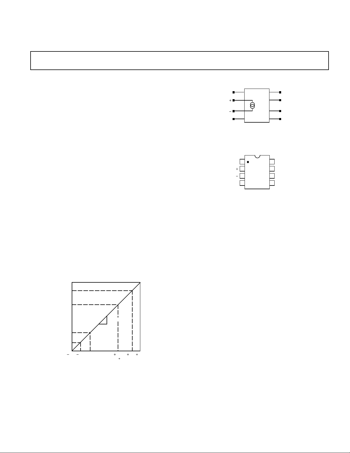
Temperature Transducer
TMP17*
FUNCTIONAL DIAGRAM
NC
V
V
NC NC
PACKAGE DIAGRAM
SO-8
NC
1
V
2
TOP VIEW
(Not to Scale)
V
3
NC
4
NC = NO CONNECT
The TMP17 is available in a low cost SO-8 surface-mount
package.
PRODUCT HIGHLIGHTS
1. A wide operating temperature range (240°C to 1105°C)
and highly linear output make the TMP17 an ideal substitute for older, more limited sensor technologies (i.e., thermistors, RTDs, diodes, thermocouples).
2. The TMP17 is electrically rugged; supply irregularities and
variations or reverse voltages up to 20 V will not damage
the device.
3. Because the TMP17 is a temperature dependent current
source, it is immune to voltage noise pickup and IR drops in
the signal leads when used remotely.
4. The high output impedance of the TMP17 provides greater
than 0.5°C/V rejection of supply voltage drift and ripple.
5. Laser wafer trimming and temperature testing insures that
TMP17 units are easily interchangeable.
6. Initial system accuracy will not degrade significantly over
time. The TMP17 has proven long term performance and
repeatability advantages inherent in integrated circuit design
and construction.
NC
NC
NC
NC
8
NC
7
NC
6
NC
5
Figure 1. Transfer Characteristic
*
Protected by U.S. Patent No. 4,123,698
REV. 0
Information furnished by Analog Devices is believed to be accurate and
reliable. However, no responsibility is assumed by Analog Devices for its
use, nor for any infringements of patents or other rights of third parties
which may result from its use. No license is granted by implication or
otherwise under any patent or patent rights of Analog Devices.
© Analog Devices, Inc., 1996
One Technology Way, P.O. Box 9106, Norwood, MA 02062-9106, U.S.A.
Tel: 617/329-4700 Fax: 617/326-8703
TMP17F/G–SPECIFICATIONS
WARNING!
ESD SENSITIVE DEVICE
(VS = 15.0 V, 2408C ≤ TA ≤ 1058C, unless otherwise noted)
Parameter Symbol Conditions Min Typ Max Units
ACCURACY
TMP17F T
TMP17G T
= 125°C
A
= 125°C
A
1
1
62.5 °C
63.5 °C
TMP17F Over Rated Temperature 63.5 °C
TMP17G Over Rated Temperature 64.5 °C
Power Supply Rejection Ratio
14 V < V
15 V < V
115 V < V
Nonlinearity Over Rated Temperature
< 15 V PSRR 0.5 °C/V
S
< 115 V PSRR 0.3 °C/V
S
< 130 V PSRR 0.3 °C/V
S
2
0.5 °C
OUTPUT
Nominal Current Output T
= 125°C (298.2K) 298.2 µA
A
Scale Factor Over Rated Temperature 1 µA/° C
Repeatability Note 3 0.2 °C
Long Term Stability T
= 1150°C for 500 Hrs
A
4
0.2 °C/month
POWER SUPPLY
Supply Range 1V
NOTES
1
An external calibration trim can be used to zero the error @ 1 25°C.
2
Defined as the maximum deviation from a mathematically best fit line.
3
Maximum deviation between 125°C readings after a temperature cycle between 2 40°C and 1105°C. Errors of this type are noncumulative.
4
Operation at 1150°C. Errors of this type are noncumulative.
Specifications subject to change without notice.
S
ABSOLUTE MAXIMUM RATINGS*
Maximum Supply Voltage . . . . . . . . . . . . . . . . . . . . . . . 130 V
Operating Temperature Range . . . . . . . . . . 240°C to 1105°C
Maximum Forward Voltage (1 to 2) . . . . . . . . . . . . . . 144 V
V+
430V
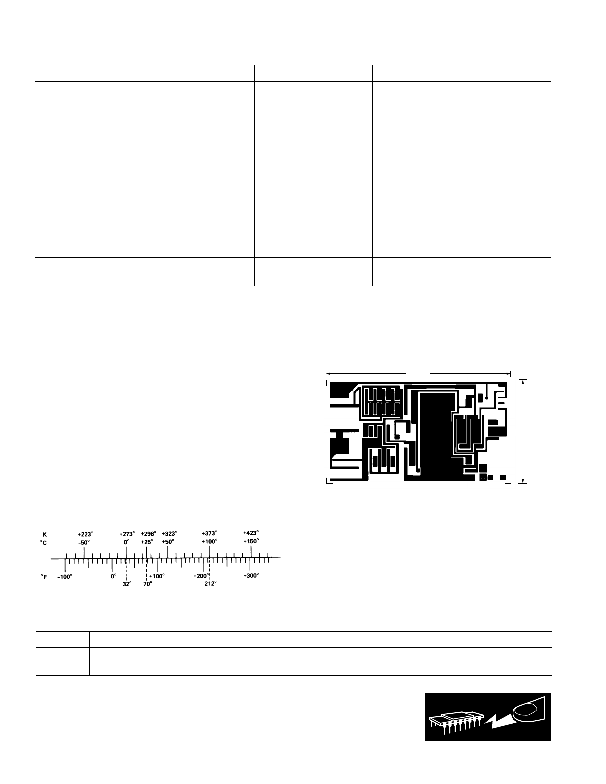
METALIZATION DIAGRAM
62MILS
Maximum Reverse Voltage (2 to 1) . . . . . . . . . . . . . . . 120 V
Dice Junction Temperature . . . . . . . . . . . . . . . . . . . . . 1175°C
Storage Temperature Range . . . . . . . . . . . . 265°C to 1160°C
Lead Temperature (Soldering, 10 sec) . . . . . . . . . . . . 1300°C
NOTES
*
Stresses above those listed under “Absolute Maximum Ratings” may cause
permanent damage to the device. This is a stress rating only and functional
operation at or above this specification is not implied. Exposure to the above
maximum rating conditions for extended periods may affect device reliability.
V–
37MILS
TEMPERATURE SCALE CONVERSION EQUATIONS
5
8C = (8F 2 32)
9
9
8F = 8C 1 32
5
K = 8C 1 273.15
ORDERING GUIDE
Model Max Cal Error @ +258C Max Error –408C to +1058C Nonlinearity –408C to +1058C Package Option
TMP17FS 2.5°C 3.5°C 0.5°C SO-8
TMP17GS 3.5°C 4.5°C 0.5°C SO-8
CAUTION
ESD (electrostatic discharge) sensitive device. Electrostatic charges as high as 4000 V readily
accumulate on the human body and test equipment and can discharge without detection.
Although the TMP17 features proprietary ESD protection circuitry, permanent damage may
occur on devices subjected to high energy electrostatic discharges. Therefore, proper ESD
precautions are recommended to avoid performance degradation or loss of functionality.
REV. 0–2–
Typical Performance Characteristics–TMP17
6
5
4
3
2
1
0
1
2
3
TEMPERATURE ERROR – C
4
5
6
50 12525
V = 5V
1
2
4
0 255075100
5
TEMPERATURE – C
MAX LIMIT
3
MIN LIMIT
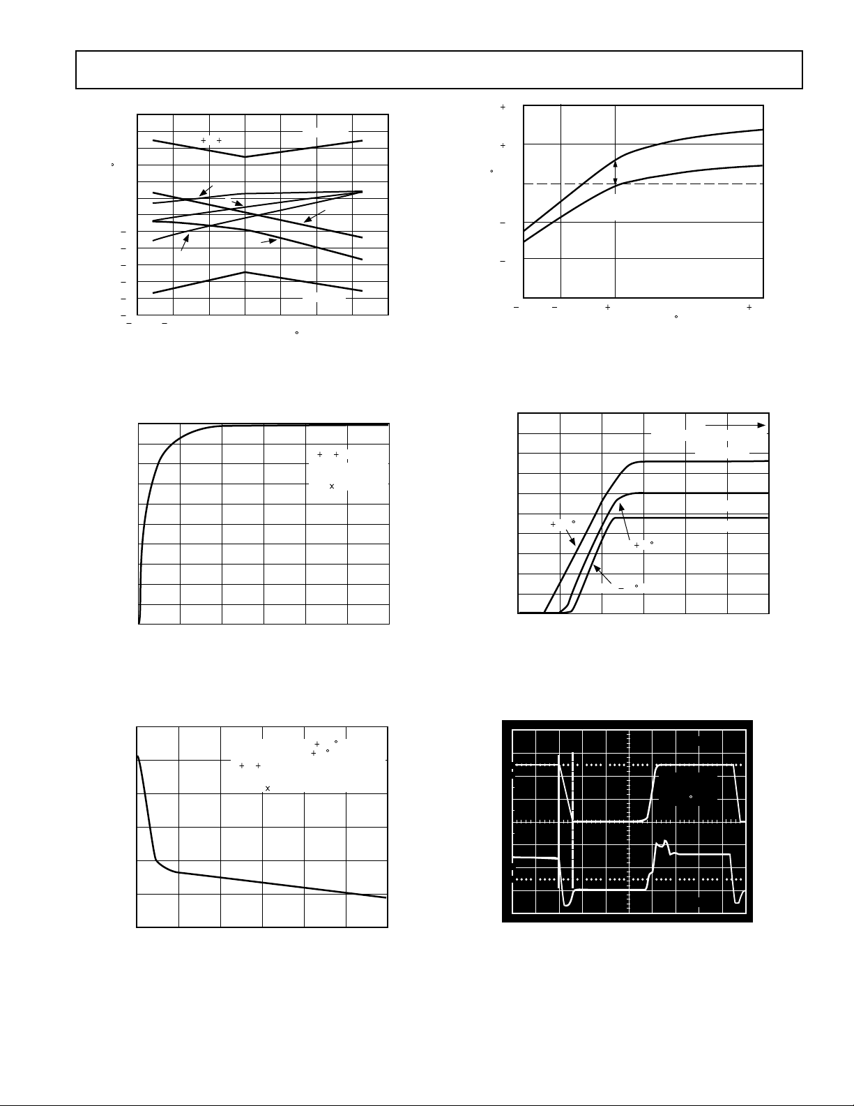
Figure 2. Accuracy vs. Temperature
100
90
80
70
60
50
40
30
PERCENT OF CHANGE – %
20
10
0
0305
10 15 20 25
TIME – sec
V = 5V
SOIC PACKAGE
SOLDERED TO
0.5"
0.3" Cu PCB
Figure 3. Thermal Response in Stirred Oil Bath
1.0
0.5
0
AFTER SINGLE
TEMPERATURE
0.5
TOTAL ERROR – C
1.0
25 10525
40
CALIBRATION
TEMPERATURE –
ACCURACY
WITHOUT TRIM
C
Figure 5. Long-Term Stability @ 1125°C
500
450
400
350
300
250
TA = 105 C
200
150
OUTPUT CURRENT – µA
100
50
0
061
TA = 40 C
2345
SUPPLY VOLTAGE – V
TA = 25 C
CONSTANT I
I
I
I
OUT
OUT
OUT
OUT
UP TO 30V
= 378µA
= 298µA
= 233µA
Figure 6. V-I Characteristics
60
TRANSITION FROM 100 C STIRRED
50
40
30
20
TIME CONSTANT – sec
10
0
0 600100
BATH TO FORCED 25 C AIR
V = 5V
SOIC PACKAGE SOLDERED
TO 0.5" 0.3" Cu PCB
200 300 400 500
AIR VELOCITY – FPM
Figure 4. Thermal Time Constant in Forced Air
REV. 0 –3–
2µs
100
90
10
0%
VIN = 0V to 5V
R
= 1kΩ,
L
= 25 C
T
A
200mV
Figure 7. Output Turn-On Settling Time

TMP17
+V
TMP17
R
100Ω
950Ω
V
OUT
= 1mV/K
THEORY OF OPERATION
The TMP17 uses a fundamental property of silicon transistors
to realize its temperature proportional output. If two identical
transistors are operated at a constant ratio of collector current
densities, r, then the difference in base-emitter voltages will be
(kT/q)(ln r). Since both k, Boltzmann’s constant, and q, the
charge of an electron, are constant, the resulting voltage is
directly Proportional To Absolute Temperature (PTAT). In the
TMP17 this difference voltage is converted to a PTAT current
by low temperature coefficient thin film resistors. This PTAT
current is then used to force the total output current to be
proportional to degrees Kelvin. The result is a current source
with an output equal to a scale factor times the temperature (K)
of the sensor. A typical V-I plot of the circuit at 125°C and the
temperature extremes is shown in Figure 6.
Factory trimming of the scale factor to 1 µA/K is accomplished
at the wafer level by adjusting the TMP17’s temperature
reading so it corresponds to the actual temperature. During
laser trimming the IC is at a temperature within a few degrees of
125°C and is powered by a 5 V supply. The device is then
packaged and automatically temperature tested to specification.
FACTORS AFFECTING TMP17 SYSTEM PRECISION
The accuracy limits given on the Specifications page for the
TMP17 make it easy to apply in a variety of diverse applications. To calculate a total error budget in a given system it is
important to correctly interpret the accuracy specifications, nonlinearity errors, the response of the circuit to supply voltage
variations and the effect of the surrounding thermal environment. As with other electronic designs external component
selection will have a major effect on accuracy.
0.2
0.1
0.1
NONLINEARITY – C
0.2
0
40 10525
0
TYPICAL NONLINEARITY
25 70
TEMPERATURE – C
Figure 8. Nonlinearity Error (TMP17)
TRIMMING FOR HIGHER ACCURACY
Calibration error at 125°C can be removed with a single
temperature trim. Figure 9 shows how to adjust the TMP17’s
scale factor in the basic voltage output circuit.
CALIBRATION ERROR, ABSOLUTE ACCURACY AND
NONLINEARITY SPECIFICATIONS
Two primary limits of error are given for the TMP17 such that
the correct grade for any given application can easily be chosen
for the overall level of accuracy required. They are the calibration accuracy at 125°C, and the error over temperature from
240°C to 1105°C. These specifications correspond to the
actual error the user would see if the current output of a
TMP17 were converted to a voltage with a precision resistor.
Note that the maximum error at room temperature or over an
extended range, including the boiling point of water, can be
directly read from the specifications table. The error limits are a
combination of initial error, scale factor variation and nonlinearity deviation from the ideal 1 µA/K output. Figure 2
graphically depicts the guaranteed limits of accuracy for a
TMP17GS.
The TMP17 has a highly linear output in comparison to older
technology sensors (i.e., thermistors, RTDs and thermocouples), thus a nonlinearity error specification is separated
from the absolute accuracy given over temperature. As a
maximum deviation from a best-fit straight line this specification
represents the only error that cannot be trimmed out. Figure 8
is a plot of typical TMP17 nonlinearity over the full rated
temperature range.
Figure 9. Basic Voltage Output (Single Temperature Trim)
To trim the circuit the temperature must be measured by a
reference sensor and the value of R should be adjusted so the
output (V
) corresponds to 1 mV/K. Note that the trim
OUT
procedure should be implemented as close as possible to the
temperature highest accuracy is desired for. In most applications
if a single temperature trim is desired it can be implemented
where the TMP17 current-to-output voltage conversion takes
place (e.g., output resistor, offset to an op amp). Figure 10
illustrates the effect on total error when using this technique.
1.0
0.5
0
AFTER SINGLE
TEMPERATURE
0.5
TOTAL ERROR – C
1.0
25 10525
40
CALIBRATION
TEMPERATURE –
ACCURACY
WITHOUT TRIM
C
Figure 10. Effect of Scale Factor Trim on Accuracy
REV. 0–4–

TMP17
If greater accuracy is desired, initial calibration and scale factor
errors can be removed by using the TMP17 in the circuit of
Figure 11.
R2
5kΩ
97.6kΩ
R1
OP196
V
= 100mV/oC
OUT
V–
REF43
+5V
8.66kΩ
7.87kΩ
1kΩ
TMP17
Figure 11. Two Temperature Trim Circuit
With the transducer at 0°C adjustment of R1 for a 0 V output
nulls the initial calibration error and shifts the output from K to
°C. Tweaking the gain of the circuit at an elevated temperature
by adjusting R2 trims out scale factor error. The only error
remaining over the temperature by adjusting R2 trims out scale
factor error. The only error remaining over the temperature
range being trimmed for its nonlinearity. A typical plot of two
trim accuracy is given in Figure 12.
SUPPLY VOLTAGE AND THERMAL ENVIRONMENT
EFFECTS
The power supply rejection characteristics of the TMP17
minimize errors due to voltage irregularity, ripple and noise. If a
supply is used other than 5 V (used in factory trimming), the
power supply error can be removed with a single temperature
trim. The PTAT nature of the TMP17 will remain unchanged.
The general insensitivity of the output allows the use of lower
cost unregulated supplies and means that a series resistance of
several hundred ohms (e.g., CMOS multiplexer, meter coil
resistance) will not degrade the overall performance.
2.0
1.0
0
ment (θJA). Self-heating error in °C can be derived by multiplying the power dissipation by θ
. Because errors of this type can
JA
vary widely for surroundings with different heat sinking capacities, it is necessary to specify θ
under several conditions.
JA
Table I shows how the magnitude of self-heating error varies
relative to the environment. In typical free air applications at
125°C with a 5 V supply the magnitude of the error is 0.2°C or
less. A small glued-on heat sink will reduce the temperature
error in high temperature, large supply voltage situations.
Table I. Thermal Characteristics
Medium θJA (8C/watt) τ (sec)*
Still Air 158 52
Moving Air @ 500 FPM 60 10
Fluorinert Liquid 35 2
NOTES
*τ is an average of one time constant (63.2% of final value). In cases where the
thermal response is not a simple exponential function, the actual thermal
response may be better than indicated.
Response of the TMP17 output to abrupt changes in ambient
temperature can be modeled by a single time constant
τ
exponential function. Figures 3 and 4 show typical response
time plots for media of interest.
The time constant, τ, is dependent on θ
and the thermal
JA
capacities of the chip and the package. Table I lists the effective
τ (time to reach 63.2% of the final value) for several different
media. Copper printed circuit board connections will sink or
conduct heat directly through the TMP17’s soldered leads.
When faster response is required a thermally conductive grease
or glue between the TMP17 and the surface temperature being
measured should be used.
MOUNTING CONSIDERATIONS
If the TMP17 is thermally attached and properly protected, it
can be used in any temperature measuring situation where the
maximum range of temperatures encountered is between 240°C
and 1105°C. Thermally conductive epoxy or glue is recommended under typical mounting conditions. In wet environments condensation at cold temperatures can cause leakage
current related errors and should be avoided by sealing the
device in nonconductive epoxy paint or conformal coating.
1.0
TOTAL ERROR – C
2.0
0
25 10525
TEMPERATURE –
7540
C
Figure 12. Typical Two Trim Accuracy
The thermal environment in which the TMP17 is used determines two performance traits: the effect of self-heating on
accuracy and the response time of the sensor to rapid changes in
temperature. In the first case, a rise in the IC junction temperature above the ambient temperature is a function of two
variables; the power consumption level of the circuit and the
thermal resistance between the chip and the ambient environ-
REV. 0 –5–
APPLICATIONS
Connecting several TMP17 devices in parallel adds the currents
through them and produces a reading proportional to the
average temperature. Series TMP17s will indicate the lowest
temperature because the coldest device limits the series current
flowing through the sensors. Both of these circuits are depicted
in Figure 13.

TMP17
+5V
+15V
TMP17
TMP17
TMP17
TMP17
333.3Ω
(0.1%)
V
(1mV/K)
T
AVG
10kΩ
(0.1%)
V
T
AVG
(10mV/K)
Figure 13. Average and Minimum Temperature
Connections
The circuit of Figure 14 demonstrates a method in which a
voltage output can be derived in a differential temperature
measurement.
+V
10kΩ
TMP17
TMP17
50kΩ
5MΩ
R1
10kΩ
–V
OP196
V
OUT
= (T1 – T2) x
o
(10mV/
C)
Figure 14. Differential Measurements
R1 can be used to trim out the inherent offset between the two
devices. By increasing the gain resistor (10 kΩ) temperature
measurements can be made with higher resolution. If the
magnitude of V1 and V2 is not the same, the difference in
power consumption between the two devices can cause a
differential self-heating error.
Cold junction compensation (CJC) used in thermocouple signal
conditioning can be implemented using a TMP17 in the circuit
configuration of Figure 15. Expensive simulated ice baths or
hard to trim, inaccurate bridge circuits are no longer required.
MEASURING
JUNCTION
Cu
Cu
R
REF43
TMP17
REFERENCE
JUNCTION
1kΩ
+7.5V
2.5V
10kΩ
100kΩ
THERMOCOUPLE
TYPE
J
K
T
E
S
R
R
G2
(1kΩ)
OP193
R
G1
APPROX.
R VALUE
52Ω
41Ω
41Ω
61Ω
6Ω
6Ω
V
OUT
Figure 15. Thermocouple Cold Junction Compensation
The circuit shown can be optimized for any ambient temperature range or thermocouple type by simply selecting the correct
value for the scaling resistor – R. The TMP17 output (1 µA/K)
times R should approximate the line best fit to the thermocouple
curve (slope in V/°C) over the most likely ambient temperature
range. Additionally, the output sensitivity can be chosen by
selecting the resistors R
and RG2 for the desired noninverting
G1
gain. The offset adjustment shown simply references the
TMP17 to °C. Note that the TC’s of the reference and the
resistors are the primary contributors to error. Temperature
rejection of 40 to 1 can be easily achieved using the above
technique.
Although the TMP17 offers a noise immune current output, it
is not compatible with process control/industrial automation
current loop standards. Figure 16 is an example of a temperature to 4–20 mA transmitter for use with 40 V, 1 kΩ systems.
In this circuit the 1 µA/K output of the TMP17 is amplified to
1 mA/°C and offset so that 4 mA is equivalent to 17°C and
20 mA is equivalent to 33°C. Rt is trimmed for proper reading
at an intermediate reference temperature. With a suitable choice
of resistors, any temperature range within the operating limits of
the TMP17 may be chosen.
+20V
OP97
12.7kΩ
10Ω
17 C ≈ 4mA
C ≈ 20µA
33
5kΩ 500Ω
1mA/ C
V
T
–20V
REF01E
TMP17
10mV/
C
35.7kΩ
C
10kΩ
5kΩ
R
T
Figure 16. Temperature to 4–20 mA Current Transmitter
Reading temperature with a TMP17 in a microprocessor based
system can be implemented with the circuit shown in Figure 17.
REF43
+5V
2.5V
R
OFFSET/RGAIN
R
R
OFFSET
R
GAIN
R
CAL
OP196
V
OUT
R
C
F
= 100mV/( C OR F)
TMP17
V–
OFFSET
≈ 9.1kΩ
≈ 9.8kΩ
R
GAIN
100kΩ
180kΩ
Figure 17. Temperature to Digital Output
By using a differential input A/D converter and choosing the
current to voltage conversion resistor correctly, any range of
temperatures (up to the 145°C span the TMP17 is rated for)
centered at any point can be measured using a minimal number
of components. In this configuration the system will resolve up
to 1°C.
REV. 0–6–

TMP17
A variable temperature controlling thermostat can easily be built
using the TMP17 in the circuit of Figure 18.
+15V
10V
TMP17
10kΩ
C
REF01E
R
HIGH
62.7kΩ
R
SET
10kΩ
R
LOW
27.3kΩ
AD790
COMPARATOR
R
HYST
C
R
PULL-UP
TEMP > SETPOINT
OUTPUT HIGH
TEMP < SETPOINT
OUTPUT LOW
(OPTIONAL)
Figure 18. Variable Temperature Thermostat
R
and R
HIGH
by the potentiometer R
determine the limits of temperature controlled
LOW
. The circuit shown operates over the
SET
temperature range 225°C to 1105°C. The reference maintains
a constant set point voltage and insures that approximately 7 V
appears across the sensor. If it is necessary to guardband for
extraneous noise, hysteresis can be added by tying a resistor
from the output to the ungrounded end of R
LOW.
Multiple remote temperatures can be measured using several
TMP17s with a CMOS multiplexer or a series of 5 V logic gates
because of the device’s current-mode output and supply-voltage
compliance range. The on-resistance of a FET switch or output
impedance of a gate will not affect the accuracy, as long as 4 V
is maintained across the transducer. Muxes and logic driving
circuits should be chosen to minimize leakage current related
errors. Figure 19 illustrates a locally controlled mux switching
the signal current from several remote TMP17s. CMOS or TTL
gates can also be used to switch the TMP17 supply voltages,
with the multiplexed signal being transmitted over a single
twisted pair to the load.
+15V –15V
V
OUT
10kΩ
S1
S2
S8
AD7501
TTL DTL TO
CMOS I/O
E
N
CHANNEL
SELECT
D
D
E
R
C
I
O
V
D
E
E
R
R
/
T
T
8
2
REMOTE
T
1
TMP17s
control which row of sensors are being measured. The maximum number of TMP17s which can be used is the product of
the number of channels of the decoder and mux.
An example circuit controlling 80 TMP17s is shown in Figure
20. A 7-bit digital word is all that is required to select one of
the sensors. The enable input of the multiplexer turns all the
sensors off for minimum dissipation while idling.
COLUMN
SELECT
+15V
4028 BCD TO DECIMAL DECODER
80 – TMP17s
ROW
SELECT
AD7501
8-CHANNEL MUX
E
N
+15V
–15V
V
10kΩ
OUT
Figure 20. Matrix Multiplexer
To convert the TMP17 output to °C or °F a single inexpensive
reference and op amp can be used as shown in Figure 21.
Although this circuit is similar to the two temperature trim
circuit shown in Figure 11, two important differences exist.
First, the gain resistor is fixed alleviating the need for an
elevated temperature trim. Acceptable accuracy can be achieved
by choosing an inexpensive resistor with the correct tolerance.
Second, the TMP17 calibration error can be trimmed out at a
known convenient temperature (i.e., room temperature) with a
single pot adjustment. This step is independent of the gain
selection.
REF43
+5V
2.5V
R
OFFSET/RGAIN
R
R
OFFSET
R
GAIN
R
CAL
OP196
V
OUT
R
C
F
= 100mV/(oC OR oF)
TMP17
V–
OFFSET
≈ 9.1kΩ
≈ 9.8kΩ
R
GAIN
100kΩ
180kΩ
Figure 21. Celsius or Fahrenheit Thermometer
Figure 19. Remote Temperature Multiplexing
To minimize the number of muxes required when a large
number of TMP17s are being used, the circuit can be configured in a matrix. That is, a decoder can be used to switch the
supply voltage to a column of TMP17s while a mux is used to
REV. 0 –7–

TMP17
OUTLINE DIMENSIONS
Dimensions shown in inches and (mm).
8-Lead Narrow-Body SOIC (SO-8)
0.1968 (5.00)
0.1890 (4.80)
8
0.1574 (4.00)
0.1497 (3.80)
5
0.2440 (6.20)
41
0.2284 (5.80)
C2154–8–7/96
PIN 1
0.0098 (0.25)
0.0040 (0.10)
SEATING
PLANE
0.0500
(1.27)
BSC
0.0688 (1.75)
0.0532 (1.35)
0.0192 (0.49)
0.0138 (0.35)
0.0098 (0.25)
0.0075 (0.19)
0.0196 (0.50)
0.0099 (0.25)
8°
0°
0.0500 (1.27)
0.0160 (0.41)
x 45°
PRINTED IN U.S.A.
REV. 0–8–
 Loading...