

±0.5°C Accurate PWM
Temperature Sensor in 5-Lead SC-70
FEATURES
Modulated serial digital output, proportional to
temperature
±0.5°C accuracy at 25°C
±1.0°C accuracy from 25°C to 70°C
Two grades available
Operation from −40°C to +150°C
Operation from 3 V to 5.5 V
Power consumption 70 µW maximum at 3.3 V
CMOS/TTL-compatible output on TMP05
Flexible open-drain output on TMP06
Small, low cost 5-lead SC-70 and SOT-23 packages
APPLICATIONS
Isolated sensors
Environmental control systems
Computer thermal monitoring
Thermal protection
Industrial process control
Power-system monitors
GENERAL DESCRIPTION
The TMP05/TMP06 are monolithic temperature sensors that
generate a modulated serial digital output (PWM), which varies
in direct proportion to the temperature of the devices. The high
period (T
while the low period (T
higher temperature accuracy of ±1°C from 0°C to 70°C with
excellent transducer linearity. The digital output of the TMP05/
TMP06 is CMOS/TTL compatible, and is easily interfaced to
the serial inputs of most popular microprocessors. The flexible
open-drain output of the TMP06 is capable of sinking 5 mA.
The TMP05/TMP06 are specified for operation at supply
voltages from 3 V to 5.5 V. Operating at 3.3 V, the supply current
is typically 370 µA. The TMP05/TMP06 are rated for operation
over the –40°C to +150°C temperature range. It is not recommended to operate these devices at temperatures above 125°C
for more than a total of 5% (5,000 hours) of the lifetime of the
devices. They are packaged in low cost, low area SC-70 and
SOT-23 packages.
) of the PWM remains static over all temperatures,
H
) varies. The B Grade version offers a
L
TMP05/TMP06
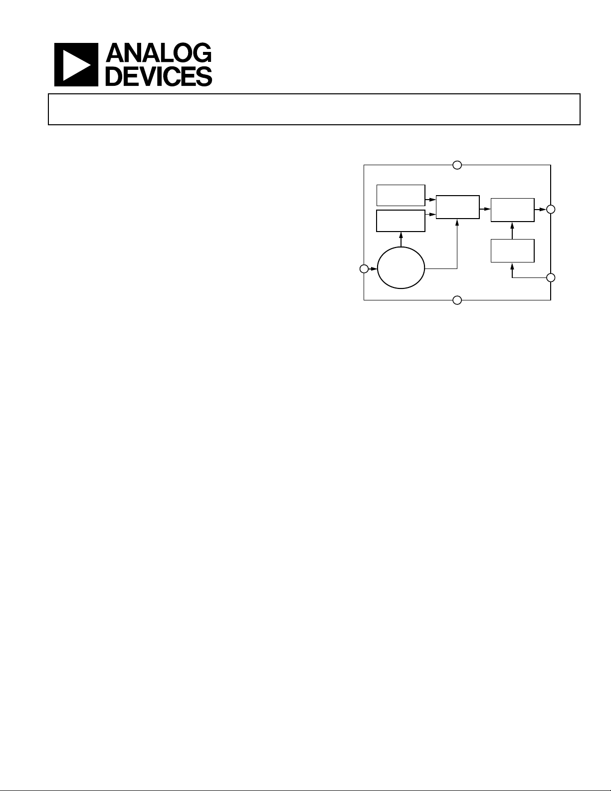
FUNCTIONAL BLOCK DIAGRAM
V
DD
5
TMP05/TMP06
TEMPERATURE
CONV/IN
2
SENSOR
REFERENCE
CLK AND
TIMING
GENERATION
Σ-∆
CORE
4
GND
Figure 1.
The TMP05/TMP06 have three modes of operation: continuously converting mode, daisy-chain mode, and one shot mode.
A three-state FUNC input determines the mode in which the
TMP05/TMP06 operate.
The CONV/IN input pin is used to determine the rate with
which the TMP05/TMP06 measure temperature in continuously converting mode and one shot mode. In daisy-chain
mode, the CONV/IN pin operates as the input to the daisy
chain.
PRODUCT HIGHLIGHTS
1. The TMP05/TMP06 have an on-chip temperature sensor
that allows an accurate measurement of the ambient
temperature. The measurable temperature range is –40°C
to +150°C.
2. Supply voltage is 3.0 V to 5.5 V.
3. Space-saving 5-lead SOT-23 and SC-70 packages.
4. Temperature accuracy is typically ±0.5°C. The part needs a
decoupling capacitor to achieve this accuracy.
5. 0.025°C temperature resolution.
6. The TMP05/TMP06 feature a one shot mode that reduces
the average power consumption to 102 µW at 1 SPS.
AVERAGING
BLOCK /
COUNTER
OUTPUT
CONTROL
1
3
OUT
FUNC
03340-0-001
Rev. 0
Information furnished by Analog Devices is believed to be accurate and reliable.
However, no responsibility is assumed by Analog Devices for its use, nor for any
infringements of patents or other rights of third parties that may result from its use.
Specifications subject to change without notice. No license is granted by implication
or otherwise under any patent or patent rights of Analog Devices. Trademarks and
registered trademarks are the property of their respective owners.
One Technology Way, P.O. Box 9106, Norwood, MA 02062-9106, U.S.A.
Tel: 781.329.4700
Fax: 781.326.8703 © 2004 Analog Devices, Inc. All rights reserved.
www.analog.com

TMP05/TMP06
TABLE OF CONTENTS
Specifications..................................................................................... 3
Operating Modes........................................................................ 13
TMP05A/TMP06A Specifications ............................................. 3
TMP05B/TMP06B Specifications .............................................. 5
Timing Characteristics ................................................................ 7
Absolute Maximum Ratings............................................................ 8
ESD Caution.................................................................................. 8
Pin Configuration and Function Descriptions............................. 9
Typical Performance Characteristics ........................................... 10
Theory of Operation ...................................................................... 13
Circuit Information.................................................................... 13
Converter Details........................................................................13
Functional Description .............................................................. 13
REVISION HISTORY
8/04—Revision 0: Initial Version
TMP05 Output ........................................................................... 16
TMP06 Output ........................................................................... 16
Application Hints ........................................................................... 17
Thermal Response Time ........................................................... 17
Self-Heating Effects.................................................................... 17
Supply Decoupling ..................................................................... 17
Temperature Monitoring........................................................... 18
Daisy-Chain Application........................................................... 18
Continuously Converting Application.................................... 23
Outline Dimensions....................................................................... 25
Ordering Guide .......................................................................... 25
Rev. 0 | Page 2 of 28

TMP05/TMP06
SPECIFICATIONS
TMP05A/TMP06A SPECIFICATIONS
All A Grade specifications apply for −40°C to +150°C; VDD decoupling capacitor is a 0.1 µF multilayer ceramic; TA = T
3.0 V to 5.5 V, unless otherwise noted.
Table 1.
Parameter Min Typ Max Unit Test Conditions/Comments
TEMPERATURE SENSOR AND ADC
Nominal Conversion Rate (One Shot Mode) See Table 7
Accuracy @ VDD = 3.3 V (3.0 V − 3.6 V) ±2 °C TA = 0°C to 70°C, VDD = 3.0 V − 3.6 V
±3 °C TA = –40°C to +70°C, VDD = 3.0 V − 3.6 V
±4 °C TA = –40°C to +125°C, VDD = 3.0 V − 3.6 V
±5
1
°C TA = –40°C to +150°C, VDD = 3.0 V − 3.6 V
Accuracy @ VDD = 5 V (4.5 V − 5.5 V) 1.5 °C TA = 0°C to 125°C, VDD = 4.5 V − 5.5 V
Temperature Resolution 0.025 °C/5 µs Step size for every 5 µs on T
TH Pulse Width 40 ms TA = 25°C, nominal conversion rate
TL Pulse Width 76 ms TA = 25°C, nominal conversion rate
Quarter Period Conversion Rate
See Table 7
(All Operating Modes)
Accuracy @ VDD = 3.3 V (3.0 V − 3.6 V) 1.5 °C TA = –40°C to +150°C
Accuracy @ VDD = 5 V (4.5 V − 5.5 V) 1.5 °C TA = 0°C to 125°C
Temperature Resolution 0.1 °C/5 µs Step size for every 5 µs on T
TH Pulse Width 10 ms TA = 25°C, QP conversion rate
TL Pulse Width 19 ms TA = 25°C, QP conversion rate
Double High/Quarter Low Conversion Rate
See Table 7
(All Operating Modes)
Accuracy @ VDD = 3.3 V (3.0 V − 3.6 V) 1.5 °C TA = –40°C to +150°C
Accuracy @ VDD = 5 V (4.5 V − 5.5 V) 1.5 °C TA = 0°C to 125°C
Temperature Resolution 0.1 °C/5 µs Step size for every 5 µs on T
TH Pulse Width 80 ms TA = 25°C, DH/QL conversion rate
TL Pulse Width 19 ms TA = 25°C, DH/QL conversion rate
Long Term Drift 0.081 °C
Drift over 10 years, if part is operated
at 55°C
SUPPLIES
Supply Voltage 3 5.5 V
Supply Current
Normal Mode2 @ 3.3 V 370 550 µA Nominal conversion rate
Normal Mode2 @ 5.0 V 425 650 µA Nominal conversion rate
Quiescent2 @ 3.3 V 3 6 µA Device not converting, output is high
Quiescent2 @ 5.0 V 5.5 10 µA Device not converting, output is high
One Shot Mode @ 1 SPS 30.9 µA
Average current @ V
conversion rate @ 25°C
37.38 µA
Average current @ V
conversion rate @ 25°C
Power Dissipation 803.33 µW
= 3.3 V, continuously converting at
V
DD
nominal conversion rates @ 25°C
1 SPS 101.9 µW
Average power dissipated for V
one shot mode @ 25°C
186.9 µW
Average power dissipated for V
one shot mode @ 25°C
to T
MIN
= 3.3 V, nominal
DD
= 5.0 V, nominal
DD
L
L
L
MAX
, VDD =
= 3.3 V,
DD
= 5.0 V,
DD
Rev. 0 | Page 3 of 28

TMP05/TMP06
Parameter Min Typ Max Unit Test Conditions/Comments
TMP05 OUTPUT (PUSH-PULL)
Output High Voltage, V
Output Low Voltage, V
Output High Current, I
Pin Capacitance 10 pF
Rise Time,5 t
Fall Time,5 t
LH
HL
RON Resistance (Low Output) 55 Ω Supply and temperature dependent
TMP06 OUTPUT (OPEN DRAIN)3
Output Low Voltage, V
Output Low Voltage, V
Pin Capacitance 10 pF
High Output Leakage Current, I
Device Turn-On Time 20 ms
Fall Time,6 t
HL
RON Resistance (Low Output) 55 Ω Supply and temperature dependent
DIGITAL INPUTS3
Input Current ±1 µA VIN = 0 V to V
Input Low Voltage, V
Input High Voltage, V
Pin Capacitance 3 10 pF
1
It is not recommended to operate the device at temperatures above 125°C for more than a total of 5% (5,000 hours) of the lifetime of the device. Any exposure beyond
this limit affects device reliability.
2
Normal mode current relates to current during TL. TMP05/TMP06 are not converting during TH, so quiescent current relates to current during TH.
3
Guaranteed by design and characterization, not production tested.
4
It is advisable to restrict the current being pulled from the TMP05 output, because any excess currents going through the die cause self-heating. As a consequence,
false temperature readings can occur.
5
Test load circuit is 100 pF to GND.
6
Test load circuit is 100 pF to GND, 10 kΩ to 5.5 V.
OL
OUT
3
OH
4
V
− 0.3 V IOH = 800 µA
DD
0.4 V IOL = 800 µA
2 mA Typ VOH = 3.17 V with VDD = 3.3 V
50 ns
50 ns
OL
OL
OH
0.4 V IOL = 1.6 mA
1.2 V IOL = 5.0 mA
0.1 5 µA PWM
= 5.5 V
OUT
30 ns
DD
IL
IH
0.3 × V
0.7 × VDD V
V
DD
Rev. 0 | Page 4 of 28

TMP05/TMP06
TMP05B/TMP06B SPECIFICATIONS
All B Grade specifications apply for –40°C to +150°C; VDD decoupling capacitor is a 0.1 µF multilayer ceramic; TA = T
3.0 V to 5.5 V, unless otherwise noted.
Table 2.
Parameter Min Typ Max Unit Test Conditions/Comments
TEMPERATURE SENSOR AND ADC
Nominal Conversion Rate (One Shot Mode) See Table 7
Accuracy1 @ VDD = 3.3 V (3.0 V – 3.6 V) ±0.5 ±1 °C TA = 25°C to 70°C, VDD = 3.0 V − 3.6 V
±1.25 °C TA = 0°C to 70°C, VDD = 3.0 V − 3.6 V
±1.5 °C TA = –40°C to +70°C, VDD = 3.0 V − 3.6 V
±2 °C TA = –40°C to +100°C, VDD = 3.0 V − 3.6 V
±2.5 °C TA = –40°C to +125°C, VDD = 3.0 V − 3.6 V
±3
2
°C TA = –40°C to +150°C, VDD = 3.0 V − 3.6 V
Accuracy @ VDD = 5.0 V (4.5 V – 5.5 V) 1.5 °C TA = 0°C to 125°C, VDD = 4.5 V − 5.5 V
Temperature Resolution 0.025 °C/5 µs Step size for every 5 µs on T
TH Pulse Width 40 ms TA = 25°C, nominal conversion rate
TL Pulse Width 76 ms TA = 25°C, nominal conversion rate
Quarter Period Conversion Rate
See Table 7
(All Operating Modes)
Accuracy @ VDD = 3.3 V (3.0 V – 3.6 V) ±1.5 °C TA = –40°C to +150°C
Accuracy @ VDD = 5.0 V (4.5 V – 5.5 V) ±1.5 °C TA = 0°C to 125°C
Temperature Resolution 0.1 °C/5 µs Step size for every 5 µs on T
TH Pulse Width 10 ms TA = 25°C, QP conversion rate
TL Pulse Width 19 ms TA = 25°C, QP conversion rate
Double High/Quarter Low Conversion Rate
See Table 7
(All Operating Modes)
Accuracy @ VDD = 3.3 V (3.0 V – 3.6 V) ±1.5 °C TA = –40°C to +150°C
Accuracy @ VDD = 5 V (4.5 V – 5.5 V) ±1.5 °C TA = 0°C to 125°C
Temperature Resolution 0.1 °C/5 µs Step size for every 5 µs on T
TH Pulse Width 80 ms TA = 25°C, DH/QL conversion rate
TL Pulse Width 19 ms TA = 25°C, DH/QL conversion rate
Long Term Drift
0.081 °C
Drift over 10 years, if part is operated at
55°C
SUPPLIES
Supply Voltage 3 5.5 V
Supply Current
Normal Mode3 @ 3.3 V 370 550 µA Nominal conversion rate
Normal Mode3 @ 5.0 V 425 650 µA Nominal conversion rate
Quiescent3 @ 3.3 V 3 6 µA Device not converting, output is high
Quiescent3 @ 5.0 V 5.5 10 µA Device not converting, output is high
One Shot Mode @ 1 SPS 30.9 µA
Average current @ V
conversion rate @ 25°C
37.38 µA
Average current @ V
conversion rate @ 25°C
Power Dissipation 803.33 µW
= 3.3 V, continuously converting at
V
DD
nominal conversion rates @ 25°C
1 SPS 101.9 µW
Average power dissipated for V
one shot mode @ 25°C
186.9 µW
Average power dissipated for V
one shot mode @ 25°C
to T
MIN
= 3.3 V, nominal
DD
= 5.0 V, nominal
DD
MAX
L
L
L
, VDD =
= 3.3 V,
DD
= 5.0 V,
DD
Rev. 0 | Page 5 of 28

TMP05/TMP06
Parameter Min Typ Max Unit Test Conditions/Comments
TMP05 OUTPUT (PUSH-PULL)
Output High Voltage, V
Output Low Voltage, V
Output High Current, I
Pin Capacitance 10 pF
Rise Time,6 t
Fall Time,6 t
LH
HL
RON Resistance (Low Output) 55 Ω Supply and temperature dependent
TMP06 OUTPUT (OPEN DRAIN)4
Output Low Voltage, V
Output Low Voltage, V
Pin Capacitance 10 pF
High Output Leakage Current, I
Device Turn-On Time 20 ms
Fall Time,7 t
HL
DIGITAL INPUTS4
Input Current ±1 µA VIN = 0 V to V
Input Low Voltage, V
Input High Voltage, V
Pin Capacitance 3 10 pF
1
The accuracy specifications for 3.0 V to 3.6 V supply range are specified to 3-sigma performance. See . Figure 22
2
It is not recommended to operate the device at temperatures above 125°C for more than a total of 5% (5,000 hours) of the lifetime of the device. Any exposure beyond
this limit affects device reliability.
3
Normal mode current relates to current during TL. TMP05/TMP06 are not converting during TH, so quiescent current relates to current during TH.
4
Guaranteed by design and characterization, not production tested.
5
It is advisable to restrict the current being pulled from the TMP05 output, because any excess currents going through the die cause self-heating. As a consequence,
false temperature readings can occur.
6
Test load circuit is 100 pF to GND.
7
Test load circuit is 100 pF to GND, 10 kΩ to 5.5 V.
OL
OUT
4
OH
5
VDD − 0.3 V IOH = 800 µA
0.4 V IOL = 800 µA
2 mA Typ VOH = 3.17 V with VDD = 3.3 V
50 ns
50 ns
OL
OL
OH
0.4 V IOL = 1.6 mA
1.2 V IOL = 5.0 mA
0.1 5 µA PWM
OUT
= 5.5 V
30 ns
DD
IL
IH
0.3 × V
0.7 × VDD V
V
DD
Rev. 0 | Page 6 of 28
TMP05/TMP06
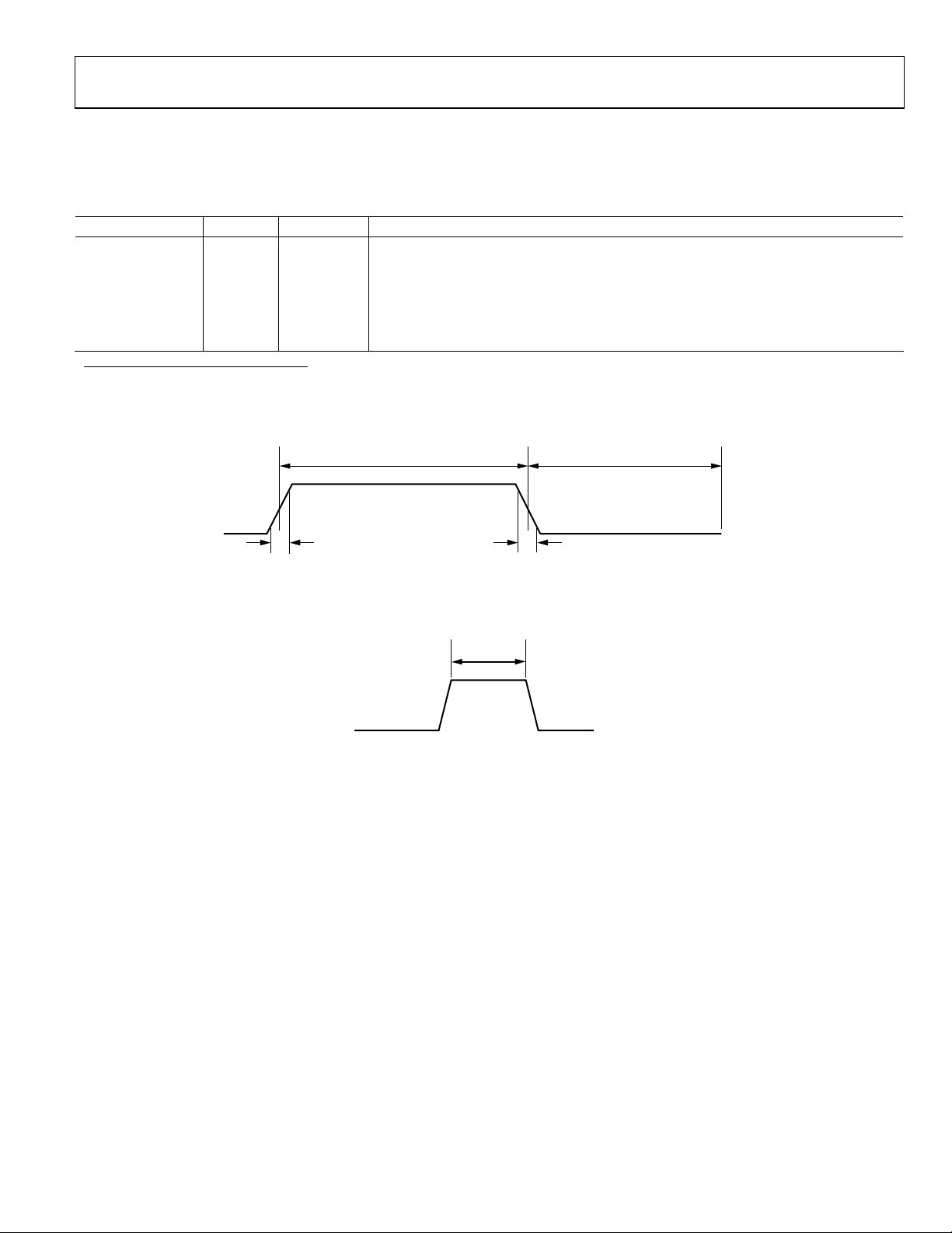
TIMING CHARACTERISTICS
TA = T
Guaranteed by design and characterization, not production tested.
Ta bl e 3.
Parameter Limit Unit Comments
TH 40 ms typ PWM high time @ 25°C under nominal conversion rate
TL 76 ms typ PWM low time @ 25°C under nominal conversion rate
1
t
3
1
t
4
2
t
4
t5 25 µs max Daisy-chain start pulse width
1
Test load circuit is 100 pF to GND.
2
Test load circuit is 100 pF to GND, 10 kΩ to 5.5 V.
MIN
to T
, VDD = 3.0 V to 5.5 V, unless otherwise noted.
MAX
50 ns typ TMP05 output rise time
50 ns typ TMP05 output fall time
30 ns typ TMP06 output fall time
T
T
H
L
t
3
90%10%
t
4
90% 10%
03340-0-002
Figure 2. PWM Output Nominal Timing Diagram (25°C)
START PULSE
t
5
03340-0-003
Figure 3. Daisy- Chain Start Timing
Rev. 0 | Page 7 of 28
TMP05/TMP06
ABSOLUTE MAXIMUM RATINGS
Table 4.
Parameter Rating
VDD to GND –0.3 V to +7 V
Digital Input Voltage to GND –0.3 V to VDD + 0.3 V
Maximum Output Current (OUT) ±10 mA
Operating Temperature Range
1
–40°C to +150°C
Storage Temperature Range –65°C to +160°C
Maximum Junction Temperature, T
JMAX
150°C
5-Lead SOT-23
Power Dissipation
2
W
= (TJ max – T
MAX
3
)/θ
A
JA
Thermal Impedance4
θJA, Junction-to-Ambient (Still Air) 240°C/W
5-Lead SC-70
Power Dissipation2 W
= (TJ max – T
MAX
3
)/θ
A
JA
Thermal Impedance4
θJA, Junction-to-Ambient 207.5°C/W
θJC, Junction-to-Case 172.3°C/W
IR Reflow Soldering
Peak Temperature 220°C (0°C/5°C)
Time at Peak Temperature 10 s to 20 s
Ramp-Up Rate 2°C/s to 3°C/s
Ramp-Down Rate –6°C/s
1
It is not recommended to operate the device at temperatures above 125°C
for more than a total of 5% (5,000 hours) of the lifetime of the device. Any
exposure beyond this limit affects device reliability.
2
SOT-23 values relate to the package being used on a 2-layer PCB and SC-70
values relate to the package being used on a 4-layer PCB. See Figure for a
plot of maximum power dissipation versus ambient temperature (T
3
TA = ambient temperature.
4
Junction-to-case resistance is applicable to components featuring a
preferential flow direction, for example, components mounted on a heat
sink. Junction-to-ambient resistance is more useful for air-cooled PCB
mounted components.
4
).
A
Stresses above those listed under Absolute Maximum Ratings
may cause permanent damage to the device. This is a stress
rating only; functional operation of the device at these or any
other conditions above those indicated in the operational
section of this specification is not implied. Exposure to absolute
maximum rating conditions for extended periods may affect
device reliability.
1.0
0.9
0.8
0.7
0.6
0.5
0.4
0.3
0.2
MAXIMUM POWER DISSIPATION (W)
0.1
0
–40 –20 0 20 40 60 80 100 120 140
SC-70
SOT-23
TEMPERATURE (°C)
Figure 4. Maximum Power Dissipation vs. Temperature
03340-0-004
ESD CAUTION
ESD (electrostatic discharge) sensitive device. Electrostatic charges as high as 4000 V readily accumulate on
the human body and test equipment and can discharge without detection. Although this product features
proprietary ESD protection circuitry, permanent damage may occur on devices subjected to high energy
electrostatic discharges. Therefore, proper ESD precautions are recommended to avoid performance
degradation or loss of functionality.
Rev. 0 | Page 8 of 28

TMP05/TMP06
PIN CONFIGURATION AND FUNCTION DESCRIPTIONS
Table 5. Pin Function Descriptions
Pin No. Mnemonic Description
1 OUT
Digital Output. Pulse-width modulated (PWM) output gives a square wave whose ratio of high to low period is
proportional to temperature.
2 CONV/IN
Digital Input. In continuously converting and one shot operating modes, a high, low, or float input determines the
temperature measurement rate. In daisy-chain operating mode, this pin is the input pin for the PWM signal from
the previous part on the daisy chain.
3 FUNC
Digital Input. A high, low, or float input on this pin gives three different modes of operation. For details, see the
Operating Modes section.
4 GND Analog and Digital Ground.
5 VDD
Positive Supply Voltage, 3.0 V to 5.5 V. Use of a decoupling capacitor of 0.1 µF as close as possible to this pin is
strongly recommended.
1
OUT
CONV/IN
FUNC
TMP05/
TMP06
2
TOP VIEW
(Not to Scale)
3
Figure 5. Pin Configuration
V
5
DD
4
GND
03340-0-005
Rev. 0 | Page 9 of 28

TMP05/TMP06
TYPICAL PERFORMANCE CHARACTERISTICS
10
9
8
7
6
5
4
3
OUTPUT FREQUENCY (Hz)
2
VDD = 3.3V
1
OUT PIN LOADED WITH 10kΩ
0
–50 –30 –10 10 30 50 70 90 110 130 150
TEMPERATURE (°C)
03340-0-020
VDD = 3.3V
C
LOAD
0
VOLTAGE (V)
1V/DIV
= 100pF
0
TIME (ns)
100ns/DIV
03340-0-023
Figure 6. PWM Output Frequency vs. Temperature
8.37
8.36
8.35
8.34
8.33
8.32
8.31
OUTPUT FREQUENCY (Hz)
OUT PIN LOADED WITH 10kΩ
8.30
AMBIENT TEMPERATURE = 25°C
8.29
3.0 5.45.14.84.54.23.93.63.3
SUPPLY VOLTAGE (V)
Figure 7. PWM Output Frequency vs. Supply Voltage
140
VDD = 3.3V
OUT PIN LOADED WITH 10kΩ
120
TL TIME
100
80
60
TIME (ms)
40
T
TIME
H
03340-0-021
VDD = 3.3V
C
LOAD
0
VOLTAGE (V)
1V/DIV
VDD = 3.3V
R
PULLUP
R
LOAD
C
LOAD
0
VOLTAGE (V)
Figure 9. TMP05 Output Rise Time at 25°C
= 100pF
0
TIME (ns)
Figure 10. TMP05 Output Fall Time at 25°C
= 1k
Ω
= 10 k
Ω
= 100pF
100ns/DIV
03340-0-024
20
0
–50 –30 –10 10 30 50 70 90 110 130 150
Figure 8. T
TEMPERATURE (°C)
and TL Times vs. Temperature
H
03340-0-022
Rev. 0 | Page 10 of 28
1V/DIV
0
TIME (ns)
Figure 11. TMP06 Output Fall Time at 25°C
100ns/DIV
03340-0-025

TMP05/TMP06
2000
VDD = 3.3V
1800
1600
1400
1200
1000
TIME (ns)
800
600
400
200
0
0 10000900080007000600050004000300020001000
CAPACTIVE LOAD (pF)
RISE TIME
FALL TIME
Figure 12. TMP05 Output Rise and Fall Times vs. Capacitive Load
250
VDD = 3.3V
200
150
I
LOAD
= 5mA
03340-0-026
1.25
VDD = 3.3V
CONTINUOUS MODE OPERATION
1.00
NOMINAL CONVERSION RATE
0.75
0.50
0.25
0
–0.25
–0.50
TEMPERATURE ERROR (°C)
–0.75
–1.00
–1.25
–40 –20 0 20 40 60 80 100 120 140
TEMPERATURE (°C)
Figure 15. Output Accuracy vs. Temperature
350
VDD = 3.3V
CONTINUOUS MODE OPERATION
300
NOMINAL CONVERSION RATE
NO LOAD ON OUT PIN
250
200
03340-0-029
100
= 1mA
I
= 0.5mA
I
OUTPUT LOW VOLTAGE (mV)
50
0
–50 –25 0 25 50 75 100 125 150
LOAD
LOAD
TEMPERATURE (°C)
Figure 13. TMP06 Output Low Voltage vs. Temperature
35
VDD = 3.3V
30
25
SINK CURRENT (mA)
20
15
–50 –25 0 25 50 75 100 125 150
TEMPERATURE (°C)
Figure 14. TMP06 Open Drain Sink Current vs. Temperature
03340-0-027
03340-0-028
150
CURRENT (µA)
100
50
0
–50 –25 0 25 50 75 100 125 150
TEMPERATURE (°C)
Figure 16. Supply Current vs. Temperature
255
AMBIENT TEMPERATURE = 25°C
CONTINUOUS MODE OPERATION
250
NOMINAL CONVERSION RATE
NO LOAD ON OUT PIN
245
240
235
230
SUPPLY CURRENT (µA)
225
220
215
2.7 5.75.45.14.84.54.23.93.63.33.0
SUPPLY VOLTAGE (V)
Figure 17. Supply Current vs. Supply Voltage
03340-0-030
03340-0-031
Rev. 0 | Page 11 of 28

TMP05/TMP06
3.5
3.0
2.5
2.0
1.5
1.0
TEMPERATURE OFFSET (°C)
0.5
VDD = 5.5V
1.25
VDD = 3.3V
AMBIENT TEMPERATURE = 25°C
1.00
0.75
= 5V
V
DD
0.50
TEMPERATURE ERROR (°C)
0.25
0
–40 –20 0 20 40 60 80 100 120 140
TEMPERATURE (°C)
Figure 18. Temperature Offset vs. Power Supply Variation from 3.3 V
140
120
100
80
60
TEMPERATURE (°C)
40
20
0
0 10203040506070
TEMPERATURE OF
ENVIRONMENT (30°C)
CHANGED HERE
FINAL TEMPERATURE = 120°C
TIME (Seconds)
Figure 19. Response to Thermal Shock
03340-0-032
03340-0-033
0
0 5 10 15 20 25 30
LOAD CURRENT (mA)
Figure 20. TMP05 Temperature Error vs. Load Current
03340-0-034
Rev. 0 | Page 12 of 28

TMP05/TMP06
THEORY OF OPERATION
CIRCUIT INFORMATION
The TMP05/TMP06 are monolithic temperature sensors that
generate a modulated serial digital output that varies in direct
proportion with the temperature of the device. An on-board
sensor generates a voltage precisely proportional to absolute
temperature, which is compared to an internal voltage reference
and is input to a precision digital modulator. The ratiometric
encoding format of the serial digital output is independent of
the clock drift errors common to most serial modulation
techniques such as voltage-to-frequency converters. Overall
accuracy for the A Grade is ±2°C from 0°C to +70°C, with
excellent transducer linearity. B Grade accuracy is ±1°C from
25°C to 70°C. The digital output of the TMP05 is CMOS/TTL
compatible, and is easily interfaced to the serial inputs of most
popular microprocessors. The open-drain output of the TMP06
is capable of sinking 5 mA.
The on-board temperature sensor has excellent accuracy and
linearity over the entire rated temperature range without
correction or calibration by the user.
The sensor output is digitized by a first-order Σ-∆ modulator,
also known as the charge balance type analog-to-digital
converter. This type of converter utilizes time-domain oversampling and a high accuracy comparator to deliver 12 bits of
effective accuracy in an extremely compact circuit.
CONVERTER DETAILS
The Σ-∆ modulator consists of an input sampler, a summing
network, an integrator, a comparator, and a 1-bit DAC. Similar
to the voltage-to-frequency converter, this architecture creates,
in effect, a negative feedback loop whose intent is to minimize
the integrator output by changing the duty cycle of the
comparator output in response to input voltage changes. The
comparator samples the output of the integrator at a much
higher rate than the input sampling frequency, which is called
oversampling. Oversampling spreads the quantization noise
over a much wider band than that of the input signal, improving
overall noise performance and increasing accuracy.
Σ-∆ MODULATOR
VOLTAGE REF
AND VPTAT
CLOCK
GENERATOR
INTEGRATOR
+
-
Figure 21. First-Order Σ-∆ Modulator
1-BIT
DAC
COMPARATOR
+
-
DIGITAL
FILTER
03340-0-006
TMP05/TMP06
OUT
(SINGLE-BIT)
The modulated output of the comparator is encoded using a
circuit technique that results in a serial digital signal with a
mark-space ratio format. This format is easily decoded by any
microprocessor into either °C or °F values, and is readily
transmitted or modulated over a single wire. More importantly,
this encoding method neatly avoids major error sources
common to other modulation techniques, because it is clockindependent.
FUNCTIONAL DESCRIPTION
The output of the TMP05/TMP06 is a square wave with a
typical period of 116 ms at 25°C (CONV/IN pin is left floating).
The high period, T
, is const ant, while the low period, TL, varies
H
with measured temperature. The output format for the nominal
conversion rate is readily decoded by the user as follows:
Temp e rature (°C) = 421 − (751 × (T
)) (1)
H/TL
T
H
Figure 22. TMP05/TMP06 Output Format
T
L
The time periods TH (high period) and TL (low period) are
values easily read by a microprocessor timer/counter port, with
the above calculations performed in software. Because both
periods are obtained consecutively using the same clock,
performing the division indicated in the previous formula
results in a ratiometric value that is independent of the exact
frequency or drift of either the originating clock of the TMP05/
TMP06 or the user’s counting clock.
OPERATING MODES
The user can program the TMP05/TMP06 to operate in three
different modes by configuring the FUNC pin on power-up as
either low, floating, or high.
Table 6. Operating Modes
FUNC Pin Operating Mode
Low One shot
Floating Continuously converting
High Daisy-chain
Continuously Converting Mode
In continuously converting mode, the TMP05/TMP06 continuously output a square wave representing temperature. The
frequency at which this square wave is output is determined by
the state of the CONV/IN pin on power-up. Any change to the
state of the CONV/IN pin after power-up is not reflected in the
parts until the TMP05/TMP06 are powered down and back up.
03340-0-007
Rev. 0 | Page 13 of 28

TMP05/TMP06
One Shot Mode
In one shot mode, the TMP05/TMP06 output one square wave
representing temperature when requested by the microcontroller. The microcontroller pulls the OUT pin low and then
releases it to indicate to the TMP05/TMP06 that an output is
required. The temperature measurement is output when the
OUT line is released by the microcontroller (see Figure 23).
µ
CONTROLLER PULLS DOWN
OUT LINE HERE
TEMP MEASUREMENT
0
Figure 23. TMP05/TMP06 One Shot OUT Pin Signal
In the TMP05 one shot mode only, an internal resistor is
switched in series with the pull-up MOSFET. The TMP05 OUT
pin has a push-pull output configuration (see Figure 24), and,
therefore, needs a series resistor to limit the current drawn on
this pin when the user pulls it low to start a temperature
conversion. This series resistance prevents any short circuit
from V
to GND, and, therefore, protects the TMP05 from
DD
short-circuit damage.
5kΩ
TMP05
Figure 24. TMP05 One Shot Mode OUT Pin Configuration
The advantages of the one shot mode include lower average
power consumption, and the microcontroller knows that the
first low-to-high transition occurs after the microcontroller
releases the OUT pin.
T
H
V+
µ
CONTROLLER RELEASES
OUT LINE HERE
T
L
TIMET
OUT
03340-0-016
03340-0-019
Conversion Rate
In continuously converting and one shot modes, the state of the
CONV/IN pin on power-up determines the rate at which the
TMP05/TMP06 measure temperature. The available conversion
rates are shown in Table 7.
Table 7. Conversion Rates
CONV/IN Pin Conversion Rate TH/TL (25°C)
Low
Quarter period
÷ 4, TL ÷ 4)
(T
H
10/19 (ms)
Floating Nominal 40/76 (ms)
High
Double high (T
Quarter low (T
x 2)
H
÷ 4)
L
80/19 (ms)
The TMP05 (push-pull output) advantage when using the high
state conversion rate (double high/quarter low) is lower power
consumption. However, the trade-off is loss of resolution on the
low time. Depending on the state of the CONV/IN pin, two
different temperature equations must be used.
The temperature equation for the low and floating states’
conversion rates is
Temp e rature (°C) = 421 − (751 × (T
)) (2)
H/TL
Table 8. Conversion Times Using Equation 2
Temperature (°C) TL (ms) Nominal Cycle Time (ms)
–40 65.2 105
–30 66.6 107
–20 68.1 108
–10 69.7 110
0 71.4 111
10 73.1 113
20 74.9 115
25 75.9 116
30 76.8 117
40 78.8 119
50 81 121
60 83.2 123
70 85.6 126
80 88.1 128
90 90.8 131
100 93.6 134
110 96.6 137
120 99.8 140
130 103.2 143
140 106.9 147
150 110.8 151
Rev. 0 | Page 14 of 28

TMP05/TMP06
The temperature equation for the high state conversion rate is
Temp e rature (°C) = 421 − (93.875 × (T
)) (3)
H/TL
Table 9. Conversion Times Using Equation 3
Temperature (°C) TL (ms) High Cycle Time (ms)
–40 16.3 96.2
–30 16.7 96.6
–20 17 97.03
–10 17.4 97.42
0 17.8 97.84
10 18.3 98.27
20 18.7 98.73
25 19 98.96
30 19.2 99.21
40 19.7 99.71
50 20.2 100.24
60 20.8 100.8
70 21.4 101.4
80 22 102.02
90 22.7 102.69
100 23.4 103.4
110 24.1 104.15
120 25 104.95
130 25.8 105.81
140 26.7 106.73
150 27.7 107.71
Daisy-Chain Mode
Setting the FUNC pin to a high state allows multiple TMP05/
TMP06s to be connected together and, therefore, allows one
input line of the microcontroller to be the sole receiver of all
temperature measurements. In this mode, the CONV/IN pin
operates as the input of the daisy chain, and conversions take
place at the nominal conversion rate of T
= 40 ms/ 76 ms
H/TL
at 25°C.
Therefore, the temperature equation for the daisy-chain mode
of operation is
Temp e rature (°C) = 421 − (751 × (T
)) (4)
H/TL
OUT
CONV/IN
TMP05/
MICRO
TMP06
#1
IN
OUT
CONV/IN
TMP05/
TMP06
#2
OUT
CONV/IN
TMP05/
TMP06
#3
OUT
CONV/IN
TMP05/
TMP06
#N
OUT
Figure 25. Daisy-Chain Structure
A second microcontroller line is needed to generate the conversion start pulse on the CONV/IN pin. The pulse width of the
start pulse should be less than 25 µs. The start pulse on the
CONV/IN pin lets the first TMP05/TMP06 part know that it
should start a conversion and output its own temperature now.
Once the part has output its own temperature, it then outputs a
start pulse for the next part on the daisy-chain link. The pulse
width of the start pulse from each TMP05/TMP06 part is
typically 17 µs.
Figure 26 shows the start pulse on the CONV/IN pin of the first
device on the daisy chain and Figure 27 shows the PWM output
by this first part.
MUST GO HIGH ONLY
AFTER START PULSE HAS
BEEN OUTPUT BY LAST
TMP05/TMP06 ON DAISY CHAIN.
START
PULSE
CONVERSION
STARTS ON
<25µs
T
0
Figure 26. Start Pulse at CONV/IN Pin of First TMP05/TMP06 Device
on Daisy Chain
THIS EDGE
TIME
03340-0-017
03340-0-009
TIME
START
PULSE
17µs
03340-0-010
#1 TEMP MEASUREMENT
T
0
Figure 27. Daisy-Chain Temperature Measurement
and Start Pulse Output from First TMP05/TMP06
Rev. 0 | Page 15 of 28

TMP05/TMP06
#1 TEMP MEASUREMENT #2 TEMP MEASUREMENT #N TEMP MEASUREMENT
T
0
Figure 28. Daisy-Chain Signal at Input to the Microcontroller
TIME
Before the start pulse reaches a TMP05/TMP06 part in the
daisy chain, the device acts as a buffer for the previous temperature measurement signals. Each part monitors the PWM signal
for the start pulse from the previous part. Once the part detects
the start pulse, it initiates a conversion and inserts the result at
the end of the daisy-chain PWM signal. It then inserts a start
pulse for the next part in the link. The final signal input to the
microcontroller should look like Figure 28. The input signal on
Pin 2 (IN) of the first daisy-chain device must remain low until
the last device has output its start pulse.
If the input on Pin 2 (IN) goes high and remains high, the
TMP05/TMP06 part powers down between 0.3 s and 1.2 s later.
The part, therefore, requires another start pulse to generate
another temperature measurement. Note that, to reduce power
dissipation through the part, it is recommended to keep Pin 2
(IN) at a high state when the part is not converting. If the IN
pin is at 0 V, then the OUT pin is at 0 V (because it is acting as a
buffer when not converting), and drawing current through
either the pull-up MOSFET (TMP05) or the pull-up resistor
(TMP06).
TMP05 OUTPUT
The TMP05 has a push-pull CMOS output (Figure 29) and
provides rail-to-rail output drive for logic interfaces. The rise
and fall times of the TMP05 output are closely matched, so that
errors caused by capacitive loading are minimized. If load
capacitance is large (for example, when driving a long cable), an
external buffer might improve accuracy.
START
PULSE
03340-0-008
An internal resistor is connected in series with the pull-up
MOSFET when the TMP05 is operating in one shot mode.
V+
OUT
TMP05
Figure 29. TMP05 Digital Output Structure
03340-0-011
TMP06 OUTPUT
The TMP06 has an open-drain output. Because the output
source current is set by the pull-up resistor, output capacitance
should be minimized in TMP06 applications. Otherwise,
unequal rise and fall times skew the pulse width and introduce
measurement errors.
OUT
TMP06
Figure 30. TMP06 Digital Output Structure
03340-0-012
Rev. 0 | Page 16 of 28

TMP05/TMP06
APPLICATION HINTS
THERMAL RESPONSE TIME
The time required for a temperature sensor to settle to a
specified accuracy is a function of the thermal mass of the
sensor and the thermal conductivity between the sensor and the
object being sensed. Thermal mass is often considered
equivalent to capacitance. Thermal conductivity is commonly
specified using the symbol Q, and can be thought of as thermal
resistance. It is commonly specified in units of degrees per watt
of power transferred across the thermal joint. Thus, the time
required for the TMP05/TMP06 to settle to the desired
accuracy is dependent on the package selected, the thermal
contact established in that particular application, and the
equivalent power of the heat source. In most applications, the
settling time is probably best determined empirically.
SELF-HEATING EFFECTS
The temperature measurement accuracy of the TMP05/TMP06
might be degraded in some applications due to self-heating.
Errors introduced are from the quiescent dissipation and power
dissipated when converting, that is, during T
these temperature errors is dependent on the thermal conductivity of the TMP05/TMP06 package, the mounting technique,
and the effects of airflow. Static dissipation in the TMP05/
TMP06 is typically 10 W operating at 3.3 V with no load. In the
5-lead SC-70 package mounted in free air, this accounts for a
temperature increase due to self-heating of
ΔT = P
× θJA = 10 µW × 211.4°C/W = 0.0021°C (5)
DISS
In addition, power is dissipated by the digital output, which is
capable of sinking 800 µA continuously (TMP05). Under an
800 µA load, the output can dissipate
= (0.4 V)(0.8 mA)((TL)/TH + TL)) (6)
P
DISS
For example, with T
= 80 ms and TH = 40 ms, the power
L
dissipation due to the digital output is approximately 0.21 mW.
In a free-standing SC-70 package, this accounts for a temperature increase due to self-heating of
ΔT = P
× θJA = 0.21 mW × 211.4°C/W = 0.044°C (7)
DISS
This temperature increase adds directly to that from the
quiescent dissipation and affects the accuracy of the TMP05/
TMP06 relative to the true ambient temperature.
. The magnitude of
L
SUPPLY DECOUPLING
The TMP05/TMP06 should be decoupled with a 0.1 µF ceramic
capacitor between V
if the TMP05/TMP06 are mounted remotely from the power
supply. Precision analog products such as the TMP05/TMP06
require a well-filtered power source. Because the TMP05/
TMP06 operate from a single supply, it might seem convenient
to simply tap into the digital logic power supply. Unfortunately,
the logic supply is often a switch-mode design, which generates
noise in the 20 kHz to 1 MHz range. In addition, fast logic gates
can generate glitches hundreds of mV in amplitude due to
wiring resistance and inductance.
If possible, the TMP05/TMP06 should be powered directly
from the system power supply. This arrangement, shown in
Figure 31, isolates the analog section from the logic switching
transients. Even if a separate power supply trace is not available,
however, generous supply bypassing reduces supply-lineinduced errors. Local supply bypassing consisting of a 0.1 µF
ceramic capacitor is critical for the temperature accuracy
specifications to be achieved. This decoupling capacitor must
be placed as close as possible to the TMP05/TMP06’s V
A recommended decoupling capacitor is Phicomp’s 100 nF,
50 V X74.
Keep the capacitor package size as small as possible, because
ESL (equivalent series inductance) increases with increasing
package size. Reducing the capacitive value below 100 nF
increases the ESR (equivalent series resistance). Use of a
capacitor with an ESL of 1 nH and an ESR of 80 mΩ is
recommended.
TTL/CMOS
LOGIC
CIRCUITS
SUPPLY
Figure 31. Use Separate Traces to Reduce Power Supply Noise
and GND. This is particularly important,
DD
0.1µF
POWER
pin.
DD
TMP05/
TMP06
03340-0-013
It is recommended that current dissipated through the device be
kept to a minimum, because it has a proportional effect on the
temperature error.
Rev. 0 | Page 17 of 28

TMP05/TMP06
T
S
0
0
TEMPERATURE MONITORING
The TMP05/TMP06 are ideal for monitoring the thermal
environment within electronic equipment. For example, the
surface-mounted package accurately reflects the exact thermal
conditions that affect nearby integrated circuits.
The TMP05/TMP06 measure and convert the temperature at
the surface of their own semiconductor chip. When the TMP05/
TMP06 are used to measure the temperature of a nearby heat
source, the thermal impedance between the heat source and the
TMP05/TMP06 must be considered. Often, a thermocouple or
other temperature sensor is used to measure the temperature of
the source, while the TMP05/TMP06 temperature is monitored
by measuring T
mined, the temperature of the heat source can be inferred from
the TMP05/TMP06 output.
One example of using the TMP05/TMP06’s unique properties is
in monitoring a high power dissipation microprocessor. The
TMP05/TMP06 part, in a surface-mounted package, is mounted
directly beneath the microprocessor’s pin grid array (PGA)
package. In a typical application, the TMP05/TMP06’s output is
connected to an ASIC, where the pulse width is measured. The
TMP05/TMP06 pulse output provides a significant advantage in
this application, because it produces a linear temperature output
while needing only one I/O pin and without requiring an ADC.
and TL. Once the thermal impedance is deter-
H
DAISY-CHAIN APPLICATION
This section provides an example of how to connect two
TMP05s in daisy-chain mode to a standard 8052 microcontroller core. The ADuC812 is the microcontroller used in the
following example and has the 8052 as its core processing
engine. Figure 32 shows how to interface to the 8052 core
device. TMP05 Program Code Example 1 shows how to
communicate from the ADuC812 to the two daisy-chained
TMP05s. This code can also be used with the ADuC831 or any
microprocessor running on an 8052 core.
Figure 32 is a diagram of the input waveform into the ADuC812
from the TMP05 daisy chain, and it shows how the code’s
variables are assigned. It should be referenced when reading
TMP05 Program Code Example 1. Application notes are
available on the Analog Devices Web site showing the TMP05
working with other types of microcontrollers.
IMER T0
TEMPSEGMENT = 1 TEMPSEGMENT = 2 TEMPSEGMENT = 3
TARTS
TEMP_HIGH0
INTO
TEMP_LOW0 TEMP_LOW1
INTO INTO
Figure 32. Reference Diagram for Software Variables
in TMP05 Program Code Example 1
TEMP_HIGH2TEMP_HIGH1
03340-0-035
.1µF
.1µF
V
DD
V
DD
TMP05 (U1)
V
OUT
DD
CONV/IN
FUNC
GND
TMP05 (U2)
V
OUT
DD
CONV/IN
GND FUNC
Figure 33 shows how the three devices are hardwired together.
Figure 34 to Figure 36 are flow charts for this program.
START
PULSE
V
DD
V
DD
T
T
H
T
0
T
(U1)
H
T
(U1)
L
0
Figure 33. Typical Daisy-Chain Application Circuit
(U1)
TL (U1)
TIME
T
(U2)
H
TIME
START
PULSE
T
(U2)
L
START
PULSE
ADuC812
P3.7
P3.2/INTO
03340-0-014
Rev. 0 | Page 18 of 28

TMP05/TMP06
DECLARE VARIABLES
INITIALIZE TIMERS
ENABLE TIMER
INTERRUPTS
SEND START
PULSE
START TIMER 0
SET-UP UART
CONVERT VARIABLES
TO FLOATS
CALCULATE
TEMPERATURE
FROM U1
TEMP U1 =
421 – (751
(TEMP_LOW0 – (TEMP_HIGH1)))
×
(TEMP_HIGH0/
SET-UP EDGE
TRIGGERED
(H-L) INTO
ENABLE INTO
INTERRUPT
ENABLE GLOBAL
INTERRUPTS
CALCULATE
TEMPERATURE
FROM U2
TEMP U2 =
421 – (751
(TEMP_LOW1 – (TEMP_HIGH2)))
×
(TEMP_HIGH1/
SEND TEMPERATURE
RESULTS
OUT OF UART
03340-0-038
Figure 35. ADuC812 Temperature Calculation Routine Flowchart
WAIT FOR
INTERRUPT
PROCESS
INTERRUPTS
WAIT FOR END
OF MEASUREMENT
CALCULATE
TEMPERATURE
AND SEND
FROM UART
03340-0-036
Figure 34. ADuC812 Main Routine Flowchart
Rev. 0 | Page 19 of 28

TMP05/TMP06
START TIMER 1
ENTER INTERRUPT
ROUTINE
NO
CHECK IF TIMER 1
IS RUNNING
COPY TIMER 1 VALUES
INTO A REGISTER
RESET TIMER 1
YES
IS TEMPSEGMENT
= 1
YE S
CALCULATE
TEMP_HIGH0
RESET TIMER 0
TO ZERO
NO
IS TEMPSEGMENT
= 2
YES
CALCULATE
TEMP_LOW0
USING TIMER 1
VALUES
CALCULATE
TEMP_HIGH1
USING TIMER 0
VALUES
RESET TIMER 0
TO ZERO
NO
IS TEMPSEGMENT
= 3
YE S
CALCULATE
TEMP_LOW1
CALCULATE
TEMP_HIGH2
USING TIMER 0
VALUES
NO
INCREMENT
TEMPSEGMENT
EXIT INTERRUPT
ROUTINE
Figure 36. ADuC812 Interrupt Routine Flowchart
TMP05 Program Code Example 1
//=============================================================================================
// Description : This program reads the temperature from 2 daisy-chained TMP05 parts.
//
// This code runs on any standard 8052 part running at 11.0592MHz.
// If an alternative core frequency is used, the only change required is an
// adjustment of the baud rate timings.
//
// P3.2 = Daisy-chain output connected to INT0.
// P3.7 = Conversion control.
// Timer0 is used in gate mode to measure the high time.
// Timer1 is triggered on a high-to-low transition of INT0 and is used to measure
// the low time.
//=============================================================================================
03340-0-037
Rev. 0 | Page 20 of 28

TMP05/TMP06
#include <stdio.h>
#include <ADuC812.h> //ADuC812 SFR definitions
void delay(int);
sbit Daisy_Start_Pulse = 0xB7; //Daisy_Start_Pulse = P3.7
sbit P3_4 = 0xB4;
long temp_high0,temp_low0,temp_high1,temp_low1,temp_high2,th,tl; //Global variables to allow
//access during ISR.
//See Figure 32.
int timer0_count=0,timer1_count=0,tempsegment=0;
void int0 () interrupt 0 //INT0 Interrupt Service Routine
{
if (TR1 == 1)
{
th = TH1;
tl = TL1;
th = TH1; //To avoid misreading timer
TL1 = 0;
TH1 = 0;
}
TR1=1; //Start timer1 running, if not running
Already
if (tempsegment == 1)
{
temp_high0 = (TH0*0x100+TL0)+(timer0_count*65536); //Convert to integer
TH0=0x00; //Reset count
TL0=0x00;
timer0_count=0;
}
if (tempsegment == 2)
{
temp_low0 = (th*0x100+tl)+(timer1_count*65536); //Convert to integer
temp_high1 = (TH0*0x100+TL0)+(timer0_count*65536); //Convert to integer
TH0=0x00; //Reset count
TL0=0x00;
timer0_count=0;
timer1_count=0;
}
if (tempsegment == 3)
{
temp_low1 = (th*0x100+tl)+(timer1_count*65536); //Convert to integer
temp_high2 = (TH0*0x100+TL0)+(timer0_count*65536);
TH0=0x00; //Reset count
TL0=0x00;
timer0_count=0;
timer1_count=0;
}
tempsegment++;
}
void timer0 () interrupt 1
{
timer0_count++; //Keep a record of timer0 overflows
}
void timer1 () interrupt 3
{
timer1_count++; //Keep a record of timer1 overflows
Rev. 0 | Page 21 of 28

TMP05/TMP06
}
void main(void)
{
double temp1=0,temp2=0;
double T1,T2,T3,T4,T5;
// Initialization
TMOD = 0x19; // Timer1 in 16-bit counter mode
// Timer0 in 16-bit counter mode
// with gate on INT0. Timer0 only counts when INTO pin // is high.
ET0 = 1; // Enable timer0 interrupts
ET1 = 1; // Enable timer1 interrupts
tempsegment = 1; // Initialize segment
Daisy_Start_Pulse = 0; // Pull P3.7 low
// Start Pulse
Daisy_Start_Pulse = 1;
Daisy_Start_Pulse = 0; //Toggle P3.7 to give start pulse
// Set T0 to count the high period
TR0 = 1; // Start timer0 running
IT0 = 1; // Interrupt0 edge triggered
EX0 = 1; // Enable interrupt
EA = 1; // Enable global interrupts
for(;;)
{
if (tempsegment == 4)
break;
}
//CONFIGURE UART
SCON = 0x52 ; // 8-bit, no parity, 1 stop bit
TMOD = 0x20 ; // Configure timer1..
TH1 = 0xFD ; // ..for 9600baud..
TR1 = 1; // ..(assuming 11.0592MHz crystal)
//Convert variables to floats for calculation
T1= temp_high0;
T2= temp_low0;
T3= temp_high1;
T4= temp_low1;
T5= temp_high2;
temp1=421-(751*(T1/(T2-T3)));
temp2=421-(751*(T3/(T4-T5)));
printf("Temp1 = %f\nTemp2 = %f\n",temp1,temp2); //Sends temperature result out UART
while (1); // END of program
}
// Delay routine
void delay(int length)
{
while (length >=0)
length--;
}
Rev. 0 | Page 22 of 28

TMP05/TMP06
CONTINUOUSLY CONVERTING APPLICATION
This section provides an example of how to connect one
TMP05 in continuously converting mode to a microchip
PIC16F876 microcontroller. Figure 37 shows how to interface to
the PIC16F876.
FIRST TEMP
MEASUREMENT
SECOND TEMP
MEASUREMENT
TMP05 Program Code Example 2 shows how to communicate
T
0
TIME
from the microchip device to the TMP05. This code can also be
used with other PICs by simply changing the include file for the
part.
PIC16F876
PA.0
TMP05
OUT
CONV/IN
Figure 37. Typical Daisy-Chain Application Circuit
3.3V
V
DD
0.1µF
GNDFUNC
TMP05 Program Code Example 2
//=============================================================================================
//
// Description : This program reads the temperature from a TMP05 part set up in continuously
// converting mode.
// This code was written for a PIC16F876, but can be easily configured to function with other
// PICs by simply changing the include file for the part.
//
// Fosc = 4MHz
// Compiled under CCS C compiler IDE version 3.4
// PWM output from TMP05 connected to PortA.0 of PIC16F876
//
//============================================================================================
#include <16F876.h> // Insert header file for the particular PIC being used
#device adc=8
#use delay(clock=4000000)
#fuses NOWDT,XT, PUT, NOPROTECT, BROWNOUT, LVP
//_______________________________Wait for high function_____________________________________
void wait_for_high() {
while(input(PIN_A0)) ; /* while high, wait for low */
while(!input(PIN_A0)); /* wait for high */
}
//______________________________Wait for low function_______________________________________
void wait_for_low() {
while(input(PIN_A0)); /* wait for high */
}
//_______________________________Main begins here____________________________________________
void main(){
long int high_time,low_time,temp;
setup_adc_ports(NO_ANALOGS);
setup_adc(ADC_OFF);
setup_spi(FALSE);
setup_timer_1 ( T1_INTERNAL | T1_DIV_BY_2); //Sets up timer to overflow after 131.07ms
03340-0-039
Rev. 0 | Page 23 of 28

TMP05/TMP06
do{
wait_for_high();
set_timer1(0); //Reset timer
wait_for_low();
high_time = get_timer1();
set_timer1(0); //Reset timer
wait_for_high();
low_time = get_timer1();
temp = 421 – ((751 * high_time)/low_time)); //Temperature equation for the high state
//Temperature value stored in temp as a long int
}while (TRUE);
}
//conversion rate.
Rev. 0 | Page 24 of 28

TMP05/TMP06
Y
OUTLINE DIMENSIONS
2.90 BSC
2.00 BSC
1.25 BSC
0
.
1
0
1.00
0.90
0.70
M
54
12
PIN 1
A
X
0.30
0.15
0.10 COPLANARIT
COMPLIANT TO JEDEC STANDARDS MO-203AA
3
0.65 BSC
2.10 BSC
1.10 MAX
SEATING
PLANE
0.22
0.08
8°
4°
0°
0.46
0.36
0.26
Figure 38. 5-Lead Thin Shrink Small Outline Transistor Package [SC-70]
(KS-5)
Dimensions shown in millimeters
1.60 BSC
1
PIN 1
1.30
1.15
0.90
0.15MAX
COMPLIANT TO JEDEC STANDARDS MO-178AA
Figure 39. 5-Lead Small Outline Transistor Package [SOT-23]
4 5
2.80 BSC
3
2
0.95 BSC
1.90
BSC
0.50
0.30
1.45 MAX
SEATING
PLANE
0.22
0.08
(RJ-5)
Dimensions shown in millimeters
10°
5°
0°
0.60
0.45
0.30
ORDERING GUIDE
Package
Option
Branding
Model
Minimum
Quantities/Reel
Temperature
1
Range
Temperature
Accuracy
2
Package
Description
TMP05AKS-500RL7 500 –40°C to +150°C ±2°C 5-Lead SC-70 KS-5 T8A
TMP05AKS-REEL 10000 –40°C to +150°C ±2°C 5-Lead SC-70 KS-5 T8A
TMP05AKS-REEL7 3000 –40°C to +150°C ±2°C 5-Lead SC-70 KS-5 T8A
TMP05ART-500RL7 500 –40°C to +150°C ±2°C 5-Lead SOT-233 RJ-5 T8A
TMP05ART-REEL 10000 –40°C to +150°C ±2°C 5-Lead SOT-233 RJ-5 T8A
TMP05ART-REEL7 3000 –40°C to +150°C ±2°C 5-Lead SOT-233 RJ-5 T8A
TMP05BKS-500RL7 500 –40°C to +150°C ±1°C 5-Lead SC-70 KS-5 T8B
TMP05BKS-REEL 10000 –40°C to +150°C ±1°C 5-Lead SC-70 KS-5 T8B
TMP05BKS-REEL7 3000 –40°C to +150°C ±1°C 5-Lead SC-70 KS-5 T8B
TMP05BRT-500RL7 500 –40°C to +150°C ±1°C 5-Lead SOT-233 RJ-5 T8B
TMP05BRT-REEL 10000 –40°C to +150°C ±1°C 5-Lead SOT-233 RJ-5 T8B
TMP05BRT-REEL7 3000 –40°C to +150°C ±1°C 5-Lead SOT-233 RJ-5 T8B
TMP05AKSZ-500RL74 500 –40°C to +150°C ±2°C 5-Lead SC-70 KS-5 T8C
TMP05AKSZ-REEL4 10000 –40°C to +150°C ±2°C 5-Lead SC-70 KS-5 T8C
TMP05AKSZ-REEL74 3000 –40°C to +150°C ±2°C 5-Lead SC-70 KS-5 T8C
TMP05ARTZ-500RL74 500 –40°C to +150°C ±2°C 5-Lead SOT-233 RJ-5 T8C
TMP05ARTZ-REEL4 10000 –40°C to +150°C ±2°C 5-Lead SOT-233 RJ-5 T8C
TMP05ARTZ-REEL74 3000 –40°C to +150°C ±2°C 5-Lead SOT-233 RJ-5 T8C
TMP05BKSZ-500RL74 500 –40°C to +150°C ±1°C 5-Lead SC-70 KS-5 T8D
TMP05BKSZ-REEL4 10000 –40°C to +150°C ±1°C 5-Lead SC-70 KS-5 T8D
TMP05BKSZ-REEL74 3000 –40°C to +150°C ±1°C 5-Lead SC-70 KS-5 T8D
TMP05BRTZ-500RL74 500 –40°C to +150°C ±1°C 5-Lead SOT-233 RJ-5 T8D
TMP05BRTZ-REEL4 10000 –40°C to +150°C ±1°C 5-Lead SOT-233 RJ-5 T8D
TMP05BRTZ-REEL74 3000 –40°C to +150°C ±1°C 5-Lead SOT-233 RJ-5 T8D
Rev. 0 | Page 25 of 28

TMP05/TMP06
Package
Option
Branding
Model
Minimum
Quantities/Reel
Temperature
1
Range
Temperature
Accuracy
2
Package
Description
TMP06AKS-500RL7 500 –40°C to +150°C ±2°C 5-Lead SC-70 KS-5 T9A
TMP06AKS-REEL 10000 –40°C to +150°C ±2°C 5-Lead SC-70 KS-5 T9A
TMP06AKS-REEL7 3000 –40°C to +150°C ±2°C 5-Lead SC-70 KS-5 T9A
TMP06ART-500RL7 500 –40°C to +150°C ±2°C 5-Lead SOT-233 RJ-5 T9A
TMP06ART-REEL 10000 –40°C to +150°C ±2°C 5-Lead SOT-233 RJ-5 T9A
TMP06ART-REEL7 3000 –40°C to +150°C ±2°C 5-Lead SOT-233 RJ-5 T9A
TMP06BKS-500RL7 500 –40°C to +150°C ±1°C 5-Lead SC-70 KS-5 T9B
TMP06BKS-REEL 10000 –40°C to +150°C ±1°C 5-Lead SC-70 KS-5 T9B
TMP06BKS-REEL7 3000 –40°C to +150°C ±1°C 5-Lead SC-70 KS-5 T9B
TMP06BRT-500RL7 500 –40°C to +150°C ±1°C 5-Lead SOT-233 RJ-5 T9B
TMP06BRT-REEL 10000 –40°C to +150°C ±1°C 5-Lead SOT-233 RJ-5 T9B
TMP06BRT-REEL7 3000 –40°C to +150°C ±1°C 5-Lead SOT-233 RJ-5 T9B
TMP06AKSZ-500RL74 500 –40°C to +150°C ±2°C 5-Lead SC-70 KS-5 T9C
TMP06AKSZ-REEL4 10000 –40°C to +150°C ±2°C 5-Lead SC-70 KS-5 T9C
TMP06AKSZ-REEL74 3000 –40°C to +150°C ±2°C 5-Lead SC-70 KS-5 T9C
TMP06ARTZ-500RL74 500 –40°C to +150°C ±2°C 5-Lead SOT-233 RJ-5 T9C
TMP06ARTZ-REEL4 10000 –40°C to +150°C ±2°C 5-Lead SOT-233 RJ-5 T9C
TMP06ARTZ-REEL74 3000 –40°C to +150°C ±2°C 5-Lead SOT-233 RJ-5 T9C
TMP06BKSZ-500RL74 500 –40°C to +150°C ±1°C 5-Lead SC-70 KS-5 T9D
TMP06BKSZ-REEL4 10000 –40°C to +150°C ±1°C 5-Lead SC-70 KS-5 T9D
TMP06BKSZ-REEL74 3000 –40°C to +150°C ±1°C 5-Lead SC-70 KS-5 T9D
TMP06BRTZ-500RL74 500 –40°C to +150°C ±1°C 5-Lead SOT-233 RJ-5 T9D
TMP06BRTZ-REEL4 10000 –40°C to +150°C ±1°C 5-Lead SOT-233 RJ-5 T9D
TMP06BRTZ-REEL74 3000 –40°C to +150°C ±1°C 5-Lead SOT-233 RJ-5 T9D
1
It is not recommended to operate the device at temperatures above 125°C for more than a total of 5% (5,000 hours) of the lifetime of the device. Any exposure beyond
this limit affects device reliability.
2
A-Grade temperature accuracy is over the 0°C to 70°C temperature range and B-Grade temperature accuracy is over the +25°C to 70°C temperature range.
3
Consult sales for availability.
4
Z = Pb-free part.
Rev. 0 | Page 26 of 28

TMP05/TMP06
NOTES
Rev. 0 | Page 27 of 28

TMP05/TMP06
NOTES
© 2004 Analog Devices, Inc. All rights reserved. Trademarks and
registered trademarks are the property of their respective owners.
D03340–0–8/04(0)
Rev. 0 | Page 28 of 28
 Loading...