


1 2 3
D
OUT
V+
GND
VPTAT
V
REF
TEMPERATURE
SENSOR
DIGITAL
MODULATOR
TMP03/TMP04
a
Serial Digital Output Thermometers
TMP03/TMP04*
FEATURES
Low Cost 3-Pin Package
Modulated Serial Digital Output
Proportional to Temperature
1.5C Accuracy (typ) from –25C to +100C
Specified –40C to +100C, Operation to 150C
Power Consumption 6.5 mW Max at 5 V
Flexible Open-Collector Output on TMP03
CMOS/TTL-Compatible Output on TMP04
Low Voltage Operation (4.5 V to 7 V)
APPLICATIONS
Isolated Sensors
Environmental Control Systems
Computer Thermal Monitoring
Thermal Protection
Industrial Process Control
Power System Monitors
GENERAL DESCRIPTION
The TMP03/TMP04 are monolithic temperature detectors that
generate a modulated serial digital output that varies in direct
proportion to the temperature of the device. An onboard sensor
generates a voltage precisely proportional to absolute temperature which is compared to an internal voltage reference and
input to a precision digital modulator. The ratiometric encoding
format of the serial digital output is independent of the clock drift
errors common to most serial modulation techniques such as
voltage-to-frequency converters. Overall accuracy is ±1.5°C
(typical) from –25°C to +100°C, with excellent transducer linearity. The digital output of the TMP04 is CMOS/TTL
compatible, and is easily interfaced to the serial inputs of most
popular microprocessors. The open-collector output of the
TMP03 is capable of sinking 5 mA. The TMP03 is best suited
for systems requiring isolated circuits utilizing optocouplers or
isolation transformers.
The TMP03 and TMP04 are specified for operation at supply
voltages from 4.5 V to 7 V. Operating from 5 V, supply current
(unloaded) is less than 1.3 mA.
The TMP03/TMP04 are rated for operation over the –40°C to
+100°C temperature range in the low cost TO-92, SO-8, and
TSSOP-8 surface mount packages. Operation extends to 150°C
with reduced accuracy.
(continued on page 4)
FUNCTIONAL BLOCK DIAGRAM
PACKAGE TYPES AVAILABLE
TO-92
TMP03/TMP04
1
2 3
V+
D
OUT
BOTTOM VIEW
(Not to Scale)
GND
SO-8 and RU-8 (TSSOP)
1
D
OUT
2
V+
3
GND
4
NC
NC = NO CONNECT
TMP03/
TMP04
TOP VIEW
(Not to Scale)
8
NC
NC
7
6
NC
5
NC
*Patent pending.
REV. A
Information furnished by Analog Devices is believed to be accurate and
reliable. However, no responsibility is assumed by Analog Devices for its
use, nor for any infringements of patents or other rights of third parties
which may result from its use. No license is granted by implication or
otherwise under any patent or patent rights of Analog Devices.
One Technology Way, P.O. Box 9106, Norwood, MA 02062-9106, U.S.A.
Tel: 781/329-4700 World Wide Web Site: http://www.analog.com
Fax: 781/326-8703 © Analog Devices, Inc., 2002

TMP03/TMP04–SPECIFICATIONS
TMP03F
(V+ = 5 V, –40C ≤ TA ≤ 100C, unless otherwise noted.)
Parameter Symbol Conditions Min Typ Max Unit
ACCURACY
Temperature Error –25°C < T
–40°C < T
< +100°C
A
< –25°C
A
1
1
1.5 4.0 °C
2.0 5.0 °C
Temperature Linearity 0.5 °C
Long-Term Stability 1000 Hours at 125°C 0.5 °C
Nominal Mark-Space Ratio T1/T2 T
= 0°C 58.8 %
A
Nominal T1 Pulsewidth T1 10 ms
Power Supply Rejection Ratio PSRR Over Rated Supply 0.7 1.4 °C/V
TA = 25°C
OUTPUTS
Output Low Voltage V
Output Low Voltage V
Output Low Voltage V
Digital Output Capacitance C
Fall Time t
OL
OL
OL
OUT
HL
I
= 1.6 mA 0.2 V
SINK
I
= 5 mA 2 V
SINK
0°C < T
I
SINK
–40°C < T
< 100°C
A
= 4 mA 2 V
< 0°C
A
(Note 2) 15 pF
See Test Load 150 ns
Device Turn-On Time 20 ms
POWER SUPPLY
Supply Range V+ 4.5 7 V
Supply Current I
NOTES
1
Maximum deviation from output transfer function over specified temperature range.
2
Guaranteed but not tested.
Specifications subject to change without notice.
SY
Unloaded 0.9 1.3 mA
Test Load
10 kΩ to 5 V Supply, 100 pF to Ground
TMP04F
(V+ = 5 V, –40C ≤ TA ≤ 100C, unless otherwise noted.)
Parameter Symbol Conditions Min Typ Max Unit
ACCURACY
Temperature Error T
= 25°C 1.0 3.0 °C
A
–25°C < T
–40°C < T
< +100°C
A
< –25°C
A
1
1
1.5 4.0 °C
2.0 5.0 °C
Temperature Linearity 0.5 °C
Long-Term Stability 1000 Hours at 125°C 0.5 °C
Nominal Mark-Space Ratio T1/T2 T
= 0°C 58.8 %
A
Nominal T1 Pulsewidth T1 10 ms
Power Supply Rejection Ratio PSRR Over Rated Supply 0.7 1.2 °C/V
TA = 25°C
OUTPUTS
Output High Voltage V
Output Low Voltage V
Digital Output Capacitance C
Fall Time t
Rise Time t
OH
OL
OUT
HL
LH
IOH = 800 µA V+ –0.4 V
IOL = 800 µA 0.4 V
(Note 2) 15 pF
See Test Load 200 ns
See Test Load 160 ns
Device Turn-On Time 20 ms
POWER SUPPLY
Supply Range V+ 4.5 7 V
Supply Current I
NOTES
1
Maximum deviation from output transfer function over specified temperature range.
2
Guaranteed but not tested.
Specifications subject to change without notice.
SY
Unloaded 0.9 1.3 mA
Test Load
100 pF to Ground
–2–
REV. A

TMP03/TMP04
WARNING!
ESD SENSITIVE DEVICE
ABSOLUTE MAXIMUM RATINGS*
Maximum Supply Voltage . . . . . . . . . . . . . . . . . . . . . . . . . 9 V
Maximum Output Current (TMP03 D
Maximum Output Current (TMP04 D
) . . . . . . . . . 50 mA
OUT
) . . . . . . . . . 10 mA
OUT
Maximum Open-Collector Output Voltage (TMP03) . . . 18 V
Operating Temperature Range . . . . . . . . . . –55°C to +150°C
Dice Junction Temperature . . . . . . . . . . . . . . . . . . . . . . 175°C
Storage Temperature Range . . . . . . . . . . . . –65°C to +160°C
Lead Temperature (Soldering, 60 sec) . . . . . . . . . . . . . 300°C
*CAUTION
1
Stresses above those listed under Absolute Maximum Ratings may cause perma-
nent damage to the device. This is a stress rating only; functional operation at or
above this specification is not implied. Exposure to the above maximum rating
conditions for extended periods may affect device reliability.
2
Digital inputs and outputs are protected, however, permanent damage may occur
on unprotected units from high-energy electrostatic fields. Keep units in conductive foam or packaging at all times until ready to use. Use proper antistatic
handling procedures.
3
Remove power before inserting or removing units from their sockets.
Package Type
TO-92 (T9) 162
SO-8 (S) 158
TSSOP (RU) 240
NOTE
1
ΘJA is specified for device in socket (worst case conditions).
JA
1
1
1
JC
Units
120 °C/W
43 °C/W
43 °C/W
ORDERING GUIDE
Accuracy Temperature
Model at 25C Range Package
TMP03FT9 ± 3.0 XIND TO-92
TMP03FS ±3.0 XIND SO-8
TMP03FRU ±3.0 XIND TSSOP-8
TMP04FT9 ± 3.0 XIND TO-92
TMP04FS ±3.0 XIND SO-8
CAUTION
ESD (electrostatic discharge) sensitive device. Electrostatic charges as high as 4000 V readily
accumulate on the human body and test equipment and can discharge without detection.
Although the TMP03 features proprietary ESD protection circuitry, permanent damage may
occur on devices subjected to high-energy electrostatic discharges. Therefore, proper ESD
precautions are recommended to avoid performance degradation or loss of functionality.
REV. A
–3–
TMP03/TMP04
(continued from page 1)
The TMP03 is a powerful, complete temperature measurement
system with digital output, on a single chip. The onboard temperature sensor follows in the footsteps of the TMP01 low
power programmable temperature controller, offering excellent
accuracy and linearity over the entire rated temperature range
without correction or calibration by the user.
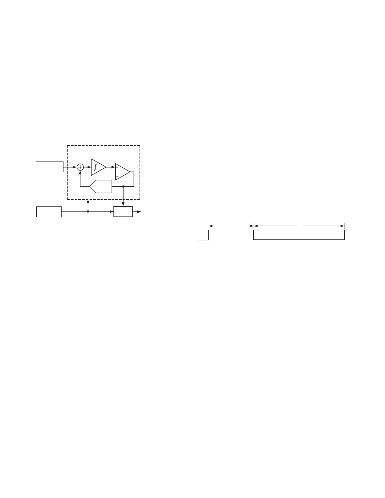
The sensor output is digitized by a first-order sigma-delta
modulator, also known as the “charge balance” type analog-todigital converter. (See Figure 1.) This type of converter utilizes
time-domain oversampling and a high accuracy comparator to
deliver 12 bits of effective accuracy in an extremely compact
circuit.
⌺⌬ MODULATOR
VOLTAGE REF
AND VPTAT
CLOCK
GENERATOR
INTEGRATOR
1-BIT
DAC
COMPARATOR
DIGITAL
FILTER
TMP03/04
OUT
(SINGLE-BIT)
Figure 1. TMP03 Block Diagram Showing First-Order
Sigma-Delta Modulator
Basically, the sigma-delta modulator consists of an input sampler, a
summing network, an integrator, a comparator, and a 1-bit
DAC. Similar to the voltage-to-frequency converter, this
architecture creates in effect a negative feedback loop whose
intent is to minimize the integrator output by changing the duty
cycle of the comparator output in response to input voltage
changes. The comparator samples the output of the integrator at
a much higher rate than the input sampling frequency, called
oversampling. This spreads the quantization noise over a much
wider band than that of the input signal, improving overall noise
performance and increasing accuracy.
The modulated output of the comparator is encoded using a
circuit technique (patent pending) which results in a serial digital signal with a mark-space ratio format that is easily decoded
by any microprocessor into either degrees centigrade or degrees
Fahrenheit values, and readily transmitted or modulated over a
single wire. Most importantly, this encoding method neatly
avoids major error sources common to other modulation techniques, as it is clock-independent.
Output Encoding
Accurate sampling of an analog signal requires precise spacing
of the sampling interval in order to maintain an accurate representation of the signal in the time domain. This dictates a
master clock between the digitizer and the signal processor. In
the case of compact, cost-effective data acquisition systems, the
addition of a buffered, high speed clock line can represent a
significant burden on the overall system design. Alternatively,
the addition of an onboard clock circuit with the appropriate
accuracy and drift performance to an integrated circuit can add
significant cost. The modulation and encoding techniques utilized in the TMP03 avoid this problem and allow the overall
circuit to fit into a compact, 3-pin package. To achieve this, a
simple, compact onboard clock and an oversampling digitizer
that is insensitive to sampling rate variations are used. Most
importantly, the digitized signal is encoded into a ratiometric
format in which the exact frequency of the TMP03’s clock is
irrelevant, and the effects of clock variations are effectively canceled upon decoding by the digital filter.
The output of the TMP03 is a square wave with a nominal
frequency of 35 Hz (±20%) at 25°C. The output format is
readily decoded by the user as follows:
T1
T2
Figure 2. TMP03 Output Format
Temperature (°C) =
Temperature (°F) =
235 −
455 −
400 ×T1
720 ×T1
T 2
T 2
The time periods T1 (high period) and T2 (low period) are
values easily read by a microprocessor timer/counter port, with
the above calculations performed in software. Since both periods are obtained consecutively, using the same clock,
performing the division indicated in the above formulas results
in a ratiometric value that is independent of the exact frequency
of, or drift in, either the originating clock of the TMP03 or the
user’s counting clock.
–4–
REV. A

TMP03/TMP04
Table I. Counter Size and Clock Frequency Effects on Quantization Error
Maximum Maximum Maximum Quantization Quantization
Count Available Temp Required Frequency Error (25C) Error (77F)
4096 125°C 94 kHz 0.284°C 0.512°F
8192 125°C 188 kHz 0.142°C 0.256°F
16384 125°C 376 kHz 0.071°C 0.128°F
Optimizing Counter Characteristics
Counter resolution, clock rate, and the resultant temperature
decode error that occurs using a counter scheme may be determined from the following calculations:
1. T1 is nominally 10 ms, and compared to T2 is relatively
insensitive to temperature changes. A useful worst-case
assumption is that T1 will never exceed 12 ms over the
specified temperature range.
T1 max = 12 ms
Substituting this value for T1 in the formula, temperature
(°C) = 235 – ([T1/T2] × 400), yields a maximum value of
T2 of 44 ms at 125°C. Rearranging the formula allows the
maximum value of T2 to be calculated at any maximum
operating temperature:
T2 (Temp) = (T1max × 400)/(235 – Temp) in seconds
2. We now need to calculate the maximum clock frequency we
can apply to the gated counter so it will not overflow during
T2 time measurement. The maximum frequency is calculated
using:
Frequency (max) = Counter Size/ (T2 at maximum
temperature)
Substituting in the equation using a 12-bit counter gives,
Fmax = 4096/44 ms ⯝ 94 kHz.
3. Now we can calculate the temperature resolution, or quantization error, provided by the counter at the chosen clock
frequency and temperature of interest. Again, using a 12-bit
counter being clocked at 90 kHz (to allow for ~5% temperature over-range), the temperature resolution at 25°C is
calculated from:
Quantization Error (
°
C) = 400 × ([Count1/Count2] –
[Count1 – 1]/[Count2 + 1])
Quantization Error (
°
F) = 720 × ([Count1/Count2] –
[Count1 – 1]/[Count2 + 1])
where, Count1 = T1max × Frequency, and Count2 =
T2 (Temp) × Frequency. At 25°C this gives a resolution of
better than 0.3°C. Note that the temperature resolution
calculated from these equations improves as temperature
increases. Higher temperature resolution will be obtained by
employing larger counters as shown in Table I. The internal
quantization error of the TMP03 sets a theoretical minimum
resolution of approximately 0.1°C at 25°C.
Self-Heating Effects
The temperature measurement accuracy of the TMP03 may be
degraded in some applications due to self-heating. Errors introduced are from the quiescent dissipation, and power dissipated
by the digital output. The magnitude of these temperature errors is dependent on the thermal conductivity of the TMP03
package, the mounting technique, and effects of airflow. Static
dissipation in the TMP03 is typically 4.5 mW operating at 5 V
with no load. In the TO-92 package mounted in free air, this
accounts for a temperature increase due to self-heating of
∆T = P
× θJA = 4.5 mW × 162°C/W = 0.73°C (1.3°F)
DISS
For a free-standing surface-mount TSSOP package, the temperature increase due to self-heating would be
∆T = P
× θJA = 4.5 mW × 240°C/W = 1.08°C (1.9°F)
DISS
In addition, power is dissipated by the digital output which is
capable of sinking 800 µA continuous (TMP04). Under full
load, the output may dissipate
P
= 0. 6 V
()
DISS
0.8 mA
()
T1 +T 2
T 2
For example, with T2 = 20 ms and T1 = 10 ms, the power
dissipation due to the digital output is approximately 0.32 mW
with a 0.8 mA load. In a free-standing TSSOP package, this
accounts for a temperature increase due to output self-heating
of
∆T = P
× ΘJA = 0.32 mW × 240°C/W = 0.08°C (0.14°F)
DISS
This temperature increase adds directly to that from the quiescent dissipation and affects the accuracy of the TMP03 relative
to the true ambient temperature. Alternatively, when the same
package has been bonded to a large plate or other thermal mass
(effectively a large heatsink) to measure its temperature, the
total self-heating error would be reduced to approximately
∆T = P
Calibration
× ΘJC = (4.5 mW + 0.32 mW) × 43°C/W = 0.21°C (0.37°F)
DISS
The TMP03 and TMP04 are laser-trimmed for accuracy and
linearity during manufacture and, in most cases, no further
adjustments are required. However, some improvement in performance can be gained by additional system calibration. To
perform a single-point calibration at room temperature, measure
the TMP03 output, record the actual measurement temperature, and modify the offset constant (normally 235; see the
Output Encoding section) as follows:
Offset Constant = 235 + (T
OBSERVED
– T
TMP03OUTPUT
)
A more complicated 2-point calibration is also possible. This
involves measuring the TMP03 output at two temperatures,
Temp1 and Temp2, and modifying the slope constant (normally
400) as follows:
Slope Constant =
T1@ Temp1
T 2@Temp1
Temp 2 −Temp1
T1@ Temp 2
−
T 2@Temp 2
where T1 and T2 are the output high and output low times,
respectively.
REV. A
–5–

TMP03/TMP04–Typical Performance Characteristics
70
60
V+ = 5V
R
LOAD
= 10k
50
40
30
20
OUTPUT FREQUENCY – Hz
10
0
–75
–25 25 75 125 175
TEMPERATURE – C
TPC 1. Output Frequency vs. Temperature
45
VS = 5V
40
R
= 10k
LOAD
TIME – ms
35
30
25
20
15
10
5
0
–75
–25 25 75 125 175
TEMPERATURE – C
T2
T1
1.05
TA = 25C
1.04
R
= 10k
LOAD
1.03
1.02
1.01
1.00
0.99
NORMALIZED OUTPUT FREQUENCY
0.98
0.97
4.5
5
5.5 6 6.5 7 7.5
SUPPLY VOLTAGE – Volts
TPC 4. Normalized Output Frequency vs. Supply Voltage
RUNNING:
50.0MS/s
TA = 25 C
V
DD
VOLTAGE SCALE = 2V/DIV
SAMPLE
( T )
= 5V
TIME SCALE = 1s/DIV
C
R
LOAD
LOAD
= 100pF
= 1k
CH 1 +WIDTH
s
Wfm DOES NOT
CROSS REF
CH 1 –WIDTH
s
Wfm DOES NOT
CROSS REF
CH 1 RISE
500ns
CH 1 FALL
s
NO VALID EDGE
TPC 2. T1 and T2 Times vs. Temperature
RUNNING:
200MS/s ET
VOLTAGE SCALE = 2V/DIV
SAMPLE
( T )
TA = 25 C
V
DD
C
LOAD
R
LOAD
TIME SCALE = 250ns/DIV
= 5V
= 100pF
= 1k
CH 1 +WIDTH
Wfm DOES NOT
CROSS REF
CH 1 –WIDTH
Wfm DOES NOT
CROSS REF
CH 1 RISE
NO VALID EDGE
CH 1 FALL
209.6ns
TPC 3. TMP03 Output Fall Time at 25°C
TPC 5. TMP03 Output Rise Time at 25°C
RUNNING:
50.0MS/s
s
s
s
TA = 125 C
V
DD
VOLTAGE SCALE = 2V/DIV
SAMPLE
( T )
= 5V
TIME SCALE = 1s/DIV
C
R
LOAD
LOAD
= 100pF
= 1k
CH 1 +WIDTH
s
Wfm DOES NOT
CROSS REF
CH 1 –WIDTH
s
Wfm DOES NOT
CROSS REF
CH 1 RISE
5380ns
CH 1 FALL
s
NO VALID EDGE
TPC 6. TMP03 Output Rise Time at 125°C
–6–
REV. A

TMP03/TMP04
= 1k
SAMPLE
( T )
CH 1 +WIDTH
s
Wfm DOES NOT
CROSS REF
CH 1 –WIDTH
s
Wfm DOES NOT
CROSS REF
CH 1 RISE
s
NO VALID EDGE
CH 1 FALL
139.5ns
EDGE SLOPE
RUNNING:
200MS/s ET
TA = 125 C
= 5V
V
DD
C
R
LOAD
LOAD
= 100pF
VOLTAGE SCALE = 2V/DIV
TIME SCALE = 250ns/DIV
TPC 7. TMP03 Output Fall Time at 125°C
= 100pF
= 0
SAMPLE
( T )
TA = 25 C
V
= 5V
DD
CH 1 +WIDTH
Wfm DOES NOT
CROSS REF
CH 1 –WIDTH
Wfm DOES NOT
CROSS REF
CH 1 RISE
NO VALID EDGE
CH 1 FALL
RUNNING:
200MS/s ET
C
LOAD
VOLTAGE SCALE = 2V/DIV
R
LOAD
s
s
s
127.6ns
= 5V
SAMPLE
( T )
C
R
LOAD
LOAD
= 100pF
= 0
CH 1 +WIDTH
Wfm DOES NOT
CROSS REF
CH 1 –WIDTH
Wfm DOES NOT
CROSS REF
CH 1 RISE
110.6ns
CH 1 FALL
NO VALID EDGE
RUNNING:
200MS/s ET
TA = 25 C
V
DD
VOLTAGE SCALE = 2V/DIV
TIME SCALE = 250ns/DIV
TPC 10. TMP04 Output Rise Time at 25°C
= 5V
SAMPLE
( T )
C
R
LOAD
LOAD
= 100pF
= 0
CH 1 +WIDTH
Wfm DOES NOT
CROSS REF
CH 1 –WIDTH
Wfm DOES NOT
CROSS REF
CH 1 RISE
149.6ns
CH 1 FALL
NO VALID EDGE
RUNNING:
200MS/s ET
TA = 125 C
V
DD
VOLTAGE SCALE = 2V/DIV
s
s
s
s
s
s
TIME SCALE = 250ns/DIV
TPC 8. TMP04 Output Fall Time at 25°C
RUNNING:
200MS/s ET
C
LOAD
VOLTAGE SCALE = 2V/DIV
R
LOAD
SAMPLE
( T )
= 100pF
= 0
TIME SCALE = 250ns/DIV
TA = 125 C
= 5V
V
DD
CH 1 +WIDTH
Wfm DOES NOT
CROSS REF
CH 1 –WIDTH
Wfm DOES NOT
CROSS REF
CH 1 RISE
NO VALID EDGE
CH 1 FALL
TPC 9. TMP04 Output Fall Time at 125°C
s
s
s
188.0ns
TIME SCALE = 250ns/DIV
TPC 11. TMP04 Output Rise Time at 125°C
2500
TA = 25C
= 5V
V
S
=
R
2000
LOAD
FAL L TIME
1500
TIME – ns
1000
RISE TIME
500
0
500
0
1000
1500
2000
2500
3000
3500 4000
4500
LOAD CAPACITANCE – pF
TPC 12. TMP04 Output Rise and Fall Times
vs. Capacitive Load
5000
REV. A
–7–

TMP03/TMP04
5
4
3
V+ = 5V
R
= 10k
2
LOAD
1
0
–1
–2
OUTPUT ACCURACY – C
–3
–4
–5
–50
–25 0
MAXIMUM LIMIT
TMP03
TMP04
MINIMUM LIMIT
25
TEMPERATURE – C
MEASUREMENTS IN
STIRRED OIL BATH
50 75 100
TPC 13. Output Accuracy vs. Temperature
OUTPUT
STARTS
LOW
OUTPUT
STARTS
HIGH
V+ = 5V
R
LOAD
= 10k
0, T2
T1
0, T1
T2
T1T2
TYPICAL VALUES
TEMP T2 T1
C ms ms
–55 15 10
25 20 10
125 35 10
125
5
START-UP VOLTAGE DEFINED AS OUTPUT READING
BEING WITHIN 5C OF OUTPUT AT 4.5V SUPPLY
4.5
R
= 10k
4
3.5
START-UP SUPPLY VOLTAGE – Volts
3
–75
LOAD
–25 25 75 125 175
TEMPERATURE – C
TPC 16. Start-Up Voltage vs. Temperature
1600
1400
1200
1000
SUPPLY CURRENT – A
800
600
400
TA = 25C
NO LOAD
V+
10 20 30 40 50
0
TIME – ms
60 70 80 90 100
TPC 14. Start-Up Response
1100
V+ = 5V
1050
NO LOAD
1000
950
900
850
SUPPLY CURRENT – A
800
750
–75
–25 25 75 125 175
TMP04
TEMPERATURE – C
TMP03
TPC 15. Supply Current vs. Temperature
200
0
1
0
3
2
SUPPLY VOLTAGE – Volts
4
5
678
TPC 17. Supply Current vs. Supply Voltage
4
V+ = 4.5V TO 7V
POWER SUPPLY REJECTION – C/V
3.5
2.5
1.5
0.5
3
2
1
0
–75
= 10k
R
LOAD
–25 25 75 125 175
TEMPERATURE – C
TPC 18. Power Supply Rejection vs. Temperature
–8–
REV. A

1
TEMPERATURE – C
2
–75
SINK CURRENT – mA
–25
25
75
125 150
8
10
12
14
V
OL
= 1V
V+ = 5V
16
20
18
6
4
TIME – sec
25
0
OUTPUT TEMPERATURE – C
10 20 30
40
50
V+ = 5V
R
LOAD =
10k
100
TRANSITION FROM STILL 25C AIR
TO STIRRED 100C OIL BATH
60
SOIC
TO –92
1.25 SEC (SOIC IN SOCKET)
2 SEC (TO –92 IN SOCKET)
V+ = 5V DC 50mV AC
R
LOAD =
0.5
TMP03/TMP04
10k
NORMAL PSSR
1k 100k 1M
FREQUENCY – Hz
10M10k
DEVIATION IN TEMPERATURE – C
–0.5
0
–1
1
100
10
TPC 19. Power Supply Rejection vs. Frequency
400
V+ = 5V
350
300
250
200
150
100
OPEN-COLLECTOR OUTPUT VOLTAGE – mV
I
LOAD
50
0
–75
–25 25 75 125 175
I
= 5mA
LOAD
= 1mA
I
= 0.5mA
LOAD
TEMPERATURE – C
TPC 22. TMP03 Open-Collector Sink Current
vs. Temperature
105
100
95
90
85
80
75
70
65
60
55
50
45
OUTPUT TEMPERATURE – C
40
35
SOIC
30
25
0
TRANSITION FROM 100C STIRRED
OIL BATH TO STILL 25C AIR
~ 23 SEC (SOIC, NO SOCKET)
~ 40 SEC (TO –92, NO SOCKET)
TO –92
25 50 75 100 125
TIME – sec
150 175
V
= 5V
S
R
10k
LOAD =
200 225 250 275 300
TPC 20. TMP03 Open-Collector Output Voltage
TPC 23. Thermal Response Time in Still Air
vs. Temperature
140
TRANSITION FROM 100C OIL BATH
120
100
80
60
40
TIME CONSTANT – sec
REV. A
20
0
0
TPC 21. Thermal Time Constant in Forced Air
TO FORCED 25C AIR
TO –92 - WITH SOCKET
TO –92 - NO SOCKET
100
200 300
AIR VELOCITY – FPM
SOIC - NO SOCKET
400
500
V+ = 5V
R
LOAD
= 10k
600 700
TPC 24. Thermal Response Time in Stirred Oil Bath
–9–

TMP03/TMP04
APPLICATIONS INFORMATION
Supply Bypassing
Precision analog products, such as the TMP03, require a wellfiltered power source. Since the TMP03 operate from a single 5
V supply, it seems convenient to simply tap into the digital logic
power supply. Unfortunately, the logic supply is often a switchmode design, which generates noise in the 20 kHz to 1 MHz
range. In addition, fast logic gates can generate glitches hundred
of millivolts in amplitude due to wiring resistance and inductance.
If possible, the TMP03 should be powered directly from the
system power supply. This arrangement, shown in Figure 3, will
isolate the analog section from the logic switching transients. Even
if a separate power supply trace is not available, however, generous supply bypassing will reduce supply-line induced errors.
Local supply bypassing consisting of a 10 µF tantalum electro-
lytic in parallel with a 0.1 µF ceramic capacitor is recommended
(Figure 4a).
TTL/CMOS
LOGIC
CIRCUITS
5V
POWER SUPPLY
+
10F
TANT
0.1F
TMP03/
TMP04
Figure 3. Use Separate Traces to Reduce Power Supply
Noise
5V
10F 0.1F
TMP03/
TMP04
5V
V+
GND
D
OUT
10F 0.1F
TMP03/
TMP04
GND
50
V+
D
OUT
a. b.
Figure 4. Recommended Supply Bypassing for the
TMP03
The quiescent power supply current requirement of the TMP03
is typically only 900 µA. The supply current will not change
appreciably when driving a light load (such as a CMOS gate), so
a simple RC filter can be added to further reduce power supply
noise (Figure 4b).
TMP03 Output Configurations
The TMP03 (Figure 5a) has an open-collector NPN output
which is suitable for driving a high current load, such as an
opto-isolator. Since the output source current is set by the pullup resistor, output capacitance should be minimized in TMP03
applications. Otherwise, unequal rise and fall times will skew the
pulsewidth and introduce measurement errors. The NPN transistor has a breakdown voltage of 18 V.
TMP03
D
OUT
TMP04
V+
D
OUT
a. b.
Figure 5. TMP03 Digital Output Structure
The TMP04 has a “totem-pole” CMOS output (Figure 5b) and
provides rail-to-rail output drive for logic interfaces. The rise
and fall times of the TMP04 output are closely matched, so that
errors caused by capacitive loading are minimized. If load capacitance is large, for example when driving a long cable, an
external buffer may improve accuracy. See the “Remote Temperature Measurement” section of this data sheet for
suggestions.
Interfacing the TMP03 to Low Voltage Logic
The TMP03’s open-collector output is ideal for driving logic
gates that operate from low supply voltages, such as 3.3 V. As
shown in Figure 6, a pull-up resistor is connected from the low
voltage logic supply (2.9 V, 3 V, etc.) to the TMP03 output.
Current through the pull-up resistor should be limited to about
1 mA, which will maintain an output LOW logic level of
<200 mV.
TMP03
5V
V+
D
GND
OUT
3.3V
3.3k
TO LOW VOLTAGE
LOGIC GATE INPUT
Figure 6. Interfacing to Low Voltage Logic
Remote Temperature Measurement
When measuring a temperature in situations where high common-mode voltages exist, an opto-isolator can be used to isolate
the output (Figure 7a). The TMP03 is recommended in this
application because its open-collector NPN transistor has a
higher current sink capability than the CMOS output of the
TMP04. To maintain the integrity of the measurement, the
opto-isolator must have relatively equal turn-on and turn-off
times. Some Darlington opto-isolators, such as the 4N32, have
a turn-off time that is much longer than their turn-on time. In
this case, the T1 time will be longer than T2, and an erroneous
reading will result. A PNP transistor can be used to provide
greater current drive to the opto-isolator (Figure 7b). An optoisolator with an integral logic gate output, such as the H11L1
from Quality Technology, can also be used (Figure 8).
–10–
REV. A

TMP03/TMP04
5V
V+
TMP03
GND
620
OPTO-COUPLER
D
OUT
V
LOGIC
4.7k
a.
5V
10k
V
LOGIC
430
V+
TMP03
GND
2N2907
OPTO-COUPLER
270
4.3k
D
OUT
b.
Figure 7. Optically Isolating the Digital Output
5V
5V
V+
TMP03
GND
680
4.7k
D
OUT
H11L1
Figure 8. An Opto-Isolator with Schmitt Trigger Logic
Gate Improves Output Rise and Fall Times
The TMP03 and TMP04 are superior to analog-output transducers for measuring temperature at remote locations, because
the digital output provides better noise immunity than an analog
signal. When measuring temperature at a remote location, the
ratio of the output pulses must be maintained. To maintain the
integrity of the pulsewidth, an external buffer can be added. For
example, adding a differential line driver such as the ADM485
permits precise temperature measurements at distances up to
4000 ft. (Figure 9). The ADM485 driver and receiver skew is
only 5 ns maximum, so the TMP04 duty cycle is not degraded.
Up to 32 ADM485s can be multiplexed onto one line by providing additional decoding.
As previously mentioned, the digital output of the TMP03
provides excellent noise immunity in remote measurement applications. The user should be aware, however, that heat from an
external cable can be conducted back to the TMP03. This heat
conduction through the connecting wires can influence the
temperature of the TMP03. If large temperature differences
exist within the sensor environment, an opto-isolator, level
shifter or other thermal barrier can be used to minimize measurement errors.
5V
V+
D
TMP04
GND
OUT
NC
5V
DE
V
CC
DI
B
A
ADM485
Figure 9. A Differential Line Driver for Remote Temperature Measurement
Microcomputer Interfaces
The TMP03 output is easily decoded with a microcomputer.
The microcomputer simply measures the T1 and T2 periods in
software or hardware, and then calculates the temperature using
the equation in the Output Encoding section of this data sheet.
Since the TMP03’s output is ratiometric, precise control of the
counting frequency is not required. The only timing requirements are that the clock frequency be high enough to provide
the required measurement resolution (see the Output Encoding
section for details) and that the clock source be stable. The
ratiometric output of the TMP03 is an advantage because the
microcomputer’s crystal clock frequency is often dictated by the
serial baud rate or other timing considerations.
Pulsewidth timing is usually done with the microcomputer’s
on-chip timer. A typical example, using the 80C51, is shown in
Figure 10. This circuit requires only one input pin on the microcomputer, which highlights the efficiency of the TMP04’s
pulsewidth output format. Traditional serial input protocols,
with data line, clock and chip select, usually require three or
more I/O pins.
5V
V+
D
TMP04
GND
OUT
INPUT
PORT 1.0
MICROCOMPUTER
TIMER 0
(16-BITS)
80C51
TIMER 1
(16-BITS)
OSC
12
TMOD REGISTER
TIMER 0 TIMER 1
TCON REGISTER
TIMER 0 TIMER 1
Figure 10. A TMP04 Interface to the 80C51 Microcomputer
The 80C51 has two 16-bit timers. The clock source for the timers
is the crystal oscillator frequency divided by 12. Thus, a crystal
frequency of 12 MHz or greater will provide resolution of 1 µs
or less.
The 80C51 timers are controlled by two dedicated registers. The
TMOD register controls the timer mode of operation, while
TCON controls the start and stop times. Both the TMOD and
TCON registers must be set to start the timer.
REV. A
–11–

TMP03/TMP04
Software for the interface is shown in Listing 1. The program
monitors the TMP04 output, and turns the counters on and off
to measure the duty cycle. The time that the output is high is mea-
Listing 1. An 80C51 Software Routine for the TMP04
;
; Test of a TMP04 interface to the 8051,
; using timer 0 and timer 1 to measure the duty cycle
;
; This program has three steps:
; 1. Clear the timer registers, then wait for a low-to; high transition on input P1.0 (which is connected
; to the output of the TMP04).
; 2. When P1.0 goes high, timer 0 starts. The program
; then loops, testing P1.0.
; 3. When P1.0 goes low, timer 0 stops & timer 1 starts. The
; program loops until P1.0 goes low, when timer 1 stops
; and the TMP04’s T1 and T2 values are stored in Special
; Function registers 8AH through 8DH (TL0 through TH1).
;
;
; Primary controls
$MOD51
$TITLE(TMP04 Interface, Using T0 and T1)
$PAGEWIDTH(80)
$DEBUG
$OBJECT
;
; Variable declarations
;
PORT1 DATA 90H ;SFR register for port 1
;TCON DATA 88H ;timer control
;TMOD DATA 89H ;timer mode
;TH0 DATA 8CH ;timer 0 hi byte
;TH1 DATA 8DH ;timer 1 hi byte
;TL0 DATA 8AH ;timer 0 lo byte
;TL1 DATA 8BH ;timer 1 low byte
;
;
ORG 100H ;arbitrary start
;
READ_TMP04: MOV A,#00 ;clear the
MOV TH0,A ; counters
MOV TH1,A ; first
MOV TL0,A ;
MOV TL1,A ;
WAIT_LO: JB PORT1.0,WAIT_LO ;wait for TMP04 output to go low
MOV A,#11H ;get ready to start timer0
MOV TMOD,A
WAIT_HI: JNB PORT1.0,WAIT_HI ;wait for output to go high
;
;Timer 0 runs while TMP04 output is high
;
SETB TCON.4 ;start timer 0
WAITTIMER0: JB PORT1.0,WAITTIMER0
CLR TCON.4 ;shut off timer 0
;
;Timer 1 runs while TMP04 output is low
;
SETB TCON.6 ;start timer 1
WAITTIMER1: JNB PORT1.0,WAITTIMER1
CLR TCON.6 ;stop timer 1
MOV A,#0H ;get ready to disable timers
MOV TMOD,A
RET
END
sured by Timer 0, and the time that the output is low is measured
by Timer 1. When the routine finishes, the results are available
in Special Function Registers (SFRs) 08AH through 08DH.
–12–
REV. A

TMP03/TMP04
When the READ_TMP04 routine is called, the counter registers
are cleared. The program sets the counters to their 16-bit mode,
and then waits for the TMP04 output to go high. When the
input port returns a logic high level, Timer 0 starts. The timer
continues to run while the program monitors the input port.
When the TMP04 output goes low, Timer 0 stops and Timer 1
starts. Timer 1 runs until the TMP04 output goes high, at which
time the TMP04 interface is complete. When the subroutine
ends, the timer values are stored in their respective SFRs and
the TMP04’s temperature can be calculated in software.
Since the 80C51 operates asynchronously to the TMP04, there
is a delay between the TMP04 output transition and the start
of the timer. This delay can vary between 0 µs and the execution
time of the instruction that recognized the transition. The
80C51’s “jump on port.bit” instructions (JB and JNB) require
24 clock cycles for execution. With a 12 MHz clock, this produces an uncertainty of 2 µs (24 clock cycles/12 MHz) at each
transition of the TMP04 output. The worst case condition occurs
when T1 is 4 µs shorter than the actual value and T2 is 4 µs
longer. For a 25°C reading (“room temperature”), the nominal
error caused by the 2 µs delay is only about ±0.15°C.
The TMP04 is also easily interfaced to digital signal processors
(DSPs), such as the ADSP210x series. Again, only a single I/O
pin is required for the interface (Figure 11).
5V
V+
D
TMP04
GND
OUT
FI (FLAG IN)
16-BIT DOWN
COUNTER
ADSP-210x
TIMER
ENABLE
10MHz
CLOCK
OSCILLATOR
n
Figure 11. Interfacing the TMP04 to the ADSP-210x Digital
Signal Processor
The ADSP2101 only has one counter, so the interface software
differs somewhat from the 80C51 example. The lack of two
counters is not a limitation, however, because the DSP architecture provides very high execution speed. The ADSP-2101
executes one instruction for each clock cycle, versus one instruction for twelve clock cycles in the 80C51, so the ADSP-2101
actually produces a more accurate conversion while using a
lower oscillator frequency.
The timer of the ADSP2101 is implemented as a down counter.
When enabled by means of a software instruction, the counter is
decremented at the clock rate divided by a programmable prescaler. Loading the value n – 1 into the prescaler register will
divide the crystal oscillator frequency by n. For the circuit of
Figure 11, therefore, loading 4 into the prescaler will divide the
10 MHz crystal oscillator by 5 and thereby decrement the counter
at a 2 MHz rate. The TMP04 output is ratiometric, of course,
so the exact clock frequency is not important.
A typical software routine for interfacing the TMP04 to the
ADSP2101 is shown in Listing 2. The program begins by initializing the prescaler and loading the counter with 0FFFF
. The
H
ADSP2101 monitors the FI flag input to establish the falling
edge of the TMP04 output, and starts the counter. When the
TMP04 output goes high, the counter is stopped. The
counter value is then subtracted from 0FFFFH to obtain the
actual number of counts, and the count is saved. Then the
counter is reloaded and runs until the TMP04 output goes low.
Finally, the TMP04 pulsewidths are converted to temperature
using the scale factor of Equation 1.
Some applications may require a hardware interface for the
TMP04. One such application could be to monitor the temperature of a high power microprocessor. The TMP04 interface
would be included as part of the system ASIC, so that the microprocessor would not be burdened with the overhead of timing
the output pulsewidths.
A typical hardware interface for the TMP04 is shown in Figure
12. The circuit measures the output pulsewidths with a resolution of ±1 µs. The TMP04 T1 and T2 periods are measured
with two cascaded 74HC4520 8-bit counters. The counters,
accumulating clock pulses from the 1 MHz external oscillator,
have a maximum period of 65 ms.
The logic interface is straightforward. On both the rising and
falling edges of the TMP04 output, an exclusive-or gate generates a pulse. This pulse triggers one half of a 74HC4538 dual
one-shot. The pulse from the one-shot is ANDed with the
TMP04 output polarity to store the counter contents in the
appropriate output registers. The falling edge of this pulse also
triggers the second one-shot, which generates a reset pulse for
the counters. After the reset pulse, the counters will begin to
count the next TMP04 output phase.
As previously mentioned, the counters have a maximum period
of 65 ms with a 1 MHz clock input. However, the TMP04’s T1
and T2 times will never exceed 32 ms. Therefore, the most
significant bit (MSB) of counter #2 will not go high in normal operation, and can be used to warn the system that an
error condition (such as a broken connection to the TMP04)
exists.
The circuit of Figure 12 will latch and save both the T1 and T2
times simultaneously. This makes the circuit suitable for debugging or test purposes as well as for a general purpose hardware
interface. In a typical ASIC application, of course, one set of
latches could be eliminated if the latch contents, and the output
polarity, were read before the next phase reversal of the TMP04.
REV. A
–13–

TMP03/TMP04
Listing 2. Software Routine for the TMP04-to-ADSP-210x Interface
;
{ ADSP-21XX Temperature Measurement Routine TEMPERAT.DSP
Altered Registers: ax0, ay0, af, ar,
si, sr0,
my0, mr0, mr1, mr2.
Return value: ar —> temperature result in 14.2 format
Computation time: 2 * TMP04 output period
}
.MODULE/RAM/BOOT=0 TEMPERAT; { Beginning TEMPERAT Program }
.ENTRY TEMPMEAS; { Entry point of this subroutine }
.CONST PRESCALER=4;
.CONST TIMFULSCALE=0Xffff;
TEMPMEAS: si=PRESCALER; { For timer prescaler }
sr0=TIMFULSCALE; { Timer counter full scale }
dm(0x3FFB)=si; { Timer Prescaler set up to 5 }
si=TIMFULSCALE; { CLKin=10MHz,Timer Period=32.768ms }
dm(0x3FFC)=si; { Timer Counter Register to 65535 }
dm(0x3FFD)=si; { Timer Period Register to 65535 }
imask=0x01; { Unmask Interrupt timer }
TEST1: if not fi jump TEST1; { Check for FI=1 }
TEST0: if fi jump TEST0; { Check for FI=0 to locate transition }
ena timer; { Enable timer, count at a 500ns rate }
COUNT2: if not fi jump COUNT2; { Check for FI=1 to stop count }
dis timer;
ay0=dm(0x3FFC); { Save counter=T2 in ALU register }
ar=sr0-ay0;
ax0=ar;
dm(0x3FFC)=si; { Reload counter at full scale }
ena timer;
COUNT1: if fi jump COUNT1; { Check for FI=0 to stop count }
dis timer;
ay0=dm(0x3FFC); { Save counter=T1 in ALU register }
ar=sr0-ay0;
my0=400;
mr=ar*my0(uu); { mr=400*T1 }
ay0=mr0; { af=MSW of dividend, ay0=LSW }
ar=mr1; af=pass ar; { ax0=16-bit divisor }
COMPUTE: astat=0; { To clear AQ flag }
divq ax0; divq ax0; { Division 400*T1/T2 }
divq ax0; divq ax0; { with 0.3 < T1/T2 < 0.7 }
divq ax0; divq ax0;
divq ax0; divq ax0;
divq ax0; divq ax0;
divq ax0; divq ax0;
divq ax0; divq ax0;
divq ax0; divq ax0;
divq ax0; divq ax0; { Result in ay0 }
ax0=0x03AC; { ax0=235*4 }
ar=ax0-ay0; { ar=235-400*T1/T2, result in øC }
rts; { format 14.2 }
.ENDMOD; { End of the subprogram }
–14–
REV. A

TMP03/TMP04
T1 DATA (MICROSECONDS) T2 DATA (MICROSECONDS)
1
OUT
10
GND
D8
15
20pF
15 14
T1 T2
GND
5V
2 5 6 9 12 15 16 19
Q1 Q2 Q3 Q4 Q5 Q6 Q7 Q8
20
V
CC
11
LE
D1 D2 D3D4D5D6D7
3 4 7 8 13 14 17 18
3.9k
5V
10
Q
9
Q
NC
8
74HC373
5V
2 5 6 9 12 15 16 19
Q1 Q2 Q3 Q4 Q5 Q6 Q7 Q8
20
V
CC
11
1
5V
2
3
1
3
2
74HC08
4
6
5
5V
16
1MHZ
CLOCK
5V
0.1F
10F
74HC373
LE
D1 D2 D3D4D5D6D7
3 4 7 8 13 14 17 18
3 4 5 6 11 12 13 14
Q0 Q1 Q2 Q3 Q0 Q1 Q2 Q3
V
CC
2
74HC4520 #1
EN
1
CLK
CLK GND RESET RESET
815
9
74HC86
4
5
10k
10
EN
10pF
OUT
GND
7
6
5V
5V
2 5 6 9 12 15 16 19
Q1 Q2 Q3 Q4 Q5 Q6 Q7 Q8
20
1
10
D8
4
5
3
V
CC
11
LE
D1 D2 D3D4D5D6D7
3 4 7 8 13 14 17 18
3456 11121314
5V
Q0 Q1 Q2 Q3 Q0 Q1 Q2 Q3
16
V
CC
2
EN
CLK
17
20pF
1k
T1 T2
V
A
CC
GND
Q
Q
8
B
CLR
74HC373
10
EN
74HC4520 #2
CLK GND RESET RESET
8
9
5V
NC
12
A
11
B
13
CLR
16
6
7
74HC4538
OUT
GND
5V
2 5 6 9 12 15 16 19
Q1 Q2 Q3 Q4 Q5 Q6 Q7 Q8
20
1
10
D8
V
CC
11
74HC373
LE
D1 D2 D3D4D5D6D7
3 4 7 8 13 14 17 18
OUT
GND
1
10
D8
V+
D
OUT
TMP04
GND
Figure 12. A Hardware Interface for the TMP04
Monitoring Electronic Equipment
The TMP03 are ideal for monitoring the thermal environment
within electronic equipment. For example, the surface-mounted
package will accurately reflect the exact thermal conditions which
affect nearby integrated circuits. The TO-92 package, on the
other hand, can be mounted above the surface of the board, to
measure the temperature of the air flowing over the board.
The TMP03 and TMP04 measure and convert the temperature
at the surface of their own semiconductor chip. When the TMP03
are used to measure the temperature of a nearby heat source,
the thermal impedance between the heat source and the TMP03
must be considered. Often, a thermocouple or other temperature sensor is used to measure the temperature of the source
while the TMP03 temperature is monitored by measuring T1
and T2. Once the thermal impedance is determined, the temperature of the heat source can be inferred from the TMP03
output.
One example of using the TMP04 to monitor a high power
dissipation microprocessor or other IC is shown in Figure 13.
The TMP04, in a surface mount package, is mounted directly
beneath the microprocessor’s pin grid array (PGA) package. In
a typical application, the TMP04’s output would be connected
to an ASIC where the pulsewidth would be measured (see the
Hardware Interface section of this data sheet for a typical interface schematic). The TMP04 pulse output provides a significant
REV. A
–15–

TMP03/TMP04
advantage in this application because it produces a linear temperature output while needing only one I/O pin and without
requiring an A/D converter.
FAST MICROPROCESSOR, DSP, ETC., IN PGA PACKAGE
PGA SOCKET
TMP04 IN SURFACE MOUNT PACKAGE
PC BOARD
Figure 13. Monitoring the Temperature of a High Power
Microprocessor Improves System Reliability
OUTLINE DIMENSIONS
Dimensions shown in inches and (mm).
Thermal Response Time
The time required for a temperature sensor to settle to a specified accuracy is a function of the thermal mass of, and the
thermal conductivity between, the sensor and the object being
sensed. Thermal mass is often considered equivalent to capacitance. Thermal conductivity is commonly specified using the
symbol Θ, and can be thought of as thermal resistance. It is
commonly specified in units of degrees per watt of power transferred across the thermal joint. Thus, the time required for the
TMP03 to settle to the desired accuracy is dependent on the
package selected, the thermal contact established in that particular application, and the equivalent power of the heat source.
In most applications, the settling time is probably best determined empirically. The TMP03 output operates at a nominal
frequency of 35 Hz at 25°C, so the minimum settling time resolution is 27 ms.
C00334–0–1/02(A)
SEATING
PLANE
0.105 (2.66)
0.095 (2.42)
0.105 (2.66)
0.080 (2.42)
0.105 (2.66)
0.080 (2.42)
3-Pin TO-92
0.135
(3.43)
MIN
0.500
(12.70)
MIN
BOTTOM
VIEW
12 3
0.205 (5.20)
0.175 (4.96)
0.210 (5.33)
0.170 (4.38)
0.050
(1.27)
MAX
0.019 (0.482)
0.016 (0.407)
SQUARE
0.055 (1.39)
0.045 (1.15)
0.165 (4.19)
0.125 (3.94)
0.1574 (4.00)
0.1497 (3.80)
PIN 1
0.0098 (0.25)
0.0040 (0.10)
SEATING
0.006 (0.15)
0.002 (0.05)
SEATING
PLANE
0.1968 (5.00)
0.1890 (4.80)
85
0.0500 (1.27)
PLANE
0.122 (3.10)
0.114 (2.90)
8
PIN 1
0.0256 (0.65)
0.0118 (0.30)
0.0075 (0.19)
8-Pin SOIC (SO-8)
0.2440 (6.20)
0.2284 (5.80)
41
BSC
0.0192 (0.49)
0.0138 (0.35)
0.0688 (1.75)
0.0532 (1.35)
0.0098 (0.25)
0.0075 (0.19)
8-Pin TSSOP (RU-8)
5
0.177 (4.50)
0.169 (4.30)
0.256 (6.50)
41
BSC
0.246 (6.25)
0.0433
(1.10)
MAX
0.0079 (0.20)
0.0035 (0.090)
0.0196 (0.50)
0.0099 (0.25)
8ⴗ
0.0500 (1.27)
0ⴗ
0.0160 (0.41)
ⴛ 45ⴗ
PRINTED IN U.S.A.
8ⴗ
0ⴗ
0.028 (0.70)
0.020 (0.50)
–16–
REV. A
 Loading...