Analog Devices MAT03EH, MAT03FH Datasheet

Low Noise, Matched
a
FEATURES
Dual Matched PNP Transistor
Low Offset Voltage: 100 V Max
Low Noise: 1 nV/√Hz @ 1 kHz Max
High Gain: 100 Min
High Gain Bandwidth: 190 MHz Typ
Tight Gain Matching: 3% Max
Excellent Logarithmic Conformance: r
GENERAL DESCRIPTION
The MAT03 dual monolithic PNP transistor offers excellent
parametric matching and high frequency performance. Low
√
noise characteristics (1 nV/
(190 MHz typical), and low offset voltage (100 µV max), makes
the MAT03 an excellent choice for demanding preamplifier applications. Tight current gain matching (3% max mismatch) and
high current gain (100 min), over a wide range of collector current, makes the MAT03 an excellent choice for current mirrors.
A low value of bulk resistance (typically 0.3 Ω) also makes the
MAT03 an ideal component for applications requiring accurate
logarithmic conformance.
Hz max @ 1 kHz), high bandwidth
⯝ 0.3 ⍀ typ
BE
Dual PNP Transistor
MAT03
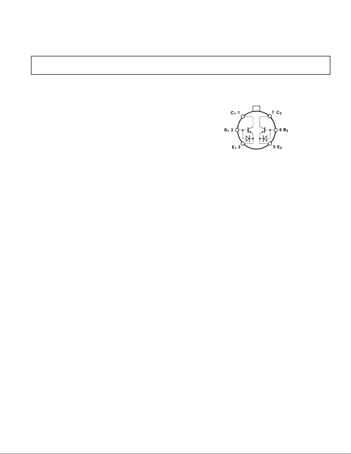
PIN CONNECTION
TO-78
(H Suffix)
Each transistor is individually tested to data sheet specifications.
Device performance is guaranteed at 25°C and over the extended
industrial and military temperature ranges. To ensure the longterm stability of the matching parameters, internal protection
diodes across the base-emitter junction clamp any reverse baseemitter junction potential. This prevents a base-emitter breakdown
condition that can result in degradation of gain and matching
performance due to excessive breakdown current.
REV. C
Information furnished by Analog Devices is believed to be accurate and
reliable. However, no responsibility is assumed by Analog Devices for its
use, nor for any infringements of patents or other rights of third parties that
may result from its use. No license is granted by implication or otherwise
under any patent or patent rights of Analog Devices.
One Technology Way, P.O. Box 9106, Norwood, MA 02062-9106, U.S.A.
Tel: 781/329-4700 www.analog.com
Fax: 781/326-8703 © Analog Devices, Inc., 2002

MAT03–SPECIFICATIONS
ELECTRICAL CHARACTERISTICS
(@ TA = 25ⴗC, unless otherwise noted.)
MAT03E MAT03F
Parameter Symbol Conditions Min Typ Max Min Typ Max Unit
Current Gain
Current Gain Matching
Offset Voltage
Offset Voltage Change ∆V
vs. Collector Voltage V
Offset Voltage Change ∆V
vs. Collector Current I
Bulk Resistance r
Offset Current I
1
3
h
FE
2
Dh
FE
V
OS
/∆V
OS
/∆I
OS
BE
OS
VCB = 0 V, –36 V
= 1 mA 100 165 80 165
I
C
= 100 µA 90 150 70 150
I
C
= 10 µA 80 120 60 120
I
C
IC = 100 µA,VCB = 0 V 0.5 3 0.5 6 %
VCB = 0 V, IC = 100 µA 40 100 40 200 µV
= 100 µA
CBIC
C
= 0 V 11 150 11 200 µV
CB1
= –36 V 11 150 11 200 µV
V
CB2
VCB = 0 V 12 50 12 75 µV
= 10 µA, IC2 = 1 mA 12 50 12 75 µV
C1
VCB = 0 V 0.3 0.75 0.3 0.75 Ω
10 µA ≤ I
≤ 1 mA 0.3 0.75 0.3 0.75 Ω
C
IC = 100 µA, VCB = 0 V 6 35 6 45 nA
Collector-Base
Leakage Current I
Noise Voltage Density4e
CB0
N
VCB = –36 V = V
MAX
IC = 1 mA, VCB = 0
= 10 Hz 0.8 0.8 nV/÷Hz
f
O
= 100 Hz 0.7 0.7 nV/÷Hz
f
O
50 200 50 400 pA
fO = 1 kHz 0.7 0.7 nV/÷ Hz
= 10 kHz 0.7 0.7 nV/÷ Hz
f
O
Collector Saturation
Voltage V
CE(SAT)
IC = 1 mA, IB = 100 µA 0.025 0.1 0.025 0.1 V
ELECTRICAL CHARACTERISTICS
(@ –40ⴗC ≤ TA ≤ 85ⴗC, unless otherwise noted.)
MAT03E MAT03F
Parameter Symbol Conditions Min Typ Max Min Typ Max Unit
Current Gain h
Offset Voltage V
Offset Voltage Drift
5
Offset Current I
Breakdown Voltage BV
NOTES
1
Current gain is measured at collector-base voltages (VCB) swept from 0 to V
2
Current gain matching (∆hFE) is defined as: ∆h
3
Offset voltage is defined as: VOS = V
4
Sample tested. Noise tested and specified as equivalent input voltage for each transistor.
5
Guaranteed by VOS test (TCVOS = VOS/T for VOS VBE) where T = 298°K for TA = 25°C.
Specifications subject to change without notice.
TCV
OS
BE1
FE
OS
OS
CEO
FE =
– V
, where VOS is the differential voltage for IC1 = IC2: VOS = V
BE2
VCB = 0 V, –36 V
= 1 mA 70 120 60 120
I
C
I
= 100 µA 60 105 50 105
C
I
= 10 µA 5090 4090
C
IC = 100 µA, VCB = 0 V 30 135 30 265 µV
IC = 100 µA, VCB = 0 V 0.3 0.5 0.3 1.0 µV/°C
IC = 100 µA, VCB = 0 V 1085 10200 nA
36 36 V
at indicated collector current. Typicals are measured at VCB = 0 V.
100 (∆IB) hFE(min )
I
C
MAX
.
I
BE1
– V
BE2
=
KT
C1
In
q
.
I
C2
–2–
REV. C

MAT03
WARNING!
ESD SENSITIVE DEVICE
ORDERING GUIDE
VOS max Temperature Package
Model (TA = +25ⴗC) Range Option
MAT03EH 100 µV –40°C to +85°C TO-78
MAT03FH 200 µV –40°C to +85°C TO-78
ABSOLUTE MAXIMUM RATINGS
Collector-Base Voltage (BV
CBO
Collector-Emitter Voltage (BV
Collector-Collector Voltage (BV
Emitter-Emitter Voltage (BV
Collector Current (I
Emitter Current (I
C
) . . . . . . . . . . . . . . . . . . . . . . . . . . . 20 mA
E
EE
) . . . . . . . . . . . . . . . . . . . . . . . . . . 20 mA
Total Power Dissipation
Ambient Temperature ≤ 70°C
Operating Temperature Range
MAT03E/F . . . . . . . . . . . . . . . . . . . . . . . . –40°C to +85°C
Operating Junction Temperature . . . . . . . . . –55°C to +150°C
Storage Temperature . . . . . . . . . . . . . . . . . . –65°C to +150°C
Lead Temperature (Soldering, 60 sec) . . . . . . . . . . . . . 300°C
Junction Temperature . . . . . . . . . . . . . . . . . –65°C to +150°C
NOTES
1
Absolute maximum ratings apply to both DICE and packaged devices.
2
Rating applies to TO-78 not using a heat sink and LCC; devices in free air only. For
TO-78, derate linearly at 6.3 mW/°C above 70°C ambient temperature; for LCC,
derate at 7.8 mW/°C.
CAUTION
ESD (electrostatic discharge) sensitive device. Electrostatic charges as high as 4000 V readily
accumulate on the human body and test equipment and can discharge without detection.
Although the MAT03 features propriety ESD protection circuitry, permanent damage may occur
on devices subjected to high-energy electrostatic discharges. Therefore, proper ESD precautions
are recommended to avoid performance degradation or loss of functionality.
1
) . . . . . . . . . . . . . . . . . . . 36 V
) . . . . . . . . . . . . . . . . . 36 V
CEO
) . . . . . . . . . . . . . . . . . 36 V
CC
) . . . . . . . . . . . . . . . . . . . 36 V
2
. . . . . . . . . . . . . . . 500 mW
REV. C
–3–

MAT03
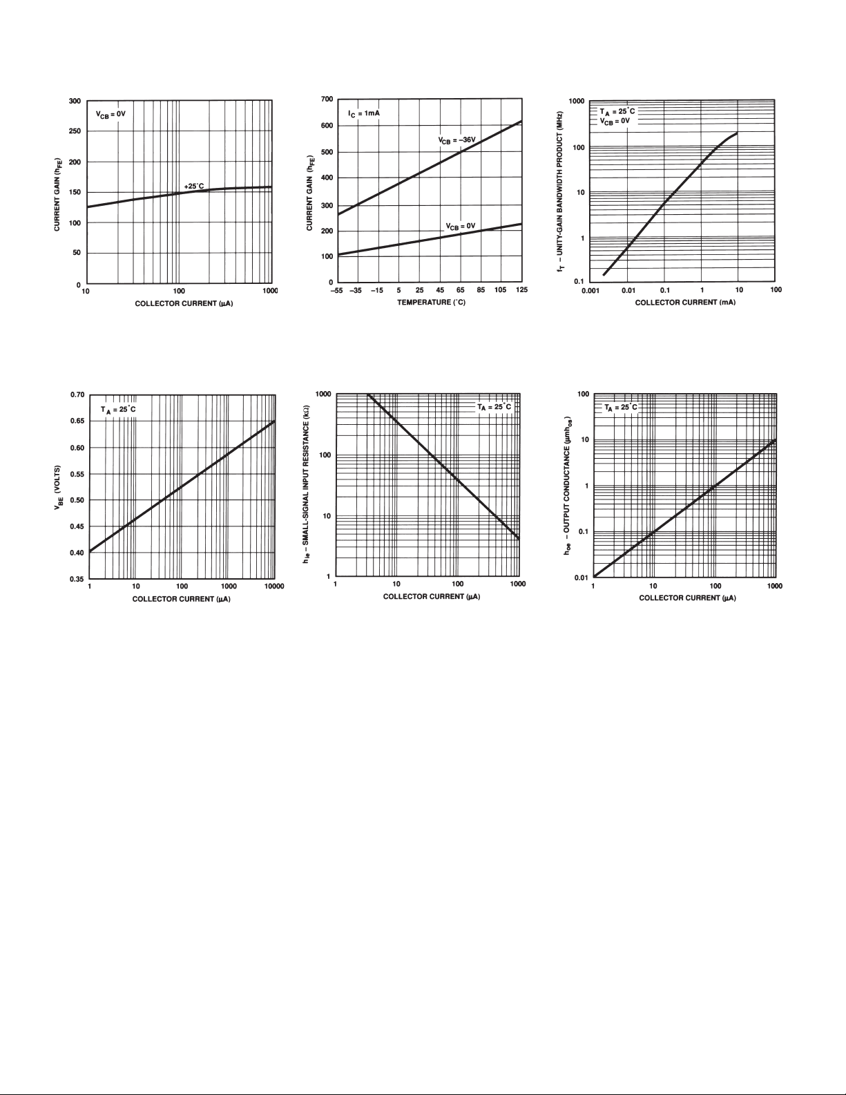
–Typical Performance Characteristics
TPC 1. Current Gain vs.
Collector Current
TPC 4. Base-Emitter Voltage
vs. Collector Current
TPC 2. Current Gain
vs. Temperature
TPC 5. Small-Signal Input Resistance
) vs. Collector Current
(h
ie
TPC 3. Gain Bandwidth vs.
Collector Current
TPC 6. Small Signal Output Conductance (h
) vs. Collector Current
oe
–4–
REV. C
 Loading...