

Page 1

Engineer-to-Engineer Note EE-229
a
Technical notes on using Analog Devices DSPs, processors and development tools
Contact our technical support at dsp.support@analog.com and at dsptools.support@analog.com
Or vi sit our o n-li ne r esou rces htt p:/ /www.analog.com/ee-notes and http://www.analog.com/processors
Estimating Power for ADSP-BF533 Blackfin® Processors
Contributed by Joe B. Rev 1 – February 20, 2004
Introduction
This EE-Note discusses the methodology for
estimating total average power consumption on
the ADSP-BF533 Blackfin® family of
processors (including the ADSP-BF531 and
ADSP-BF532 derivatives). The following
documentation will detail how to interpret power
measurements published in the processor data
sheet and how to extrapolate data for individual
sets of operating conditions based on measured
data at specific operating conditions. A “worstcase” scenario is also made available as an
example for board designers to consider when
designing their power supplies.
Average Power Consumption
Total average power consumption (P
sum of the average power dissipated in each of
the three power domains in a Blackfin
application: internal supply (
supply (
supply (V
V
), and, optionally, Real-Time Clock
DDEXT
). There are different supply
DDRTC
V
DDINT
voltages because the core does not operate at the
same voltage as the I/O. The core operates within
the range of 0.8-1.32V with a nominal rating of
1.2V (
V
). The I/O circuitry supports a range
DDINT
of 2.25-3.6V with a nominal rating of 2.5V or
3.3V (
V
), depending on the system. The Real-
DDEXT
Time Clock can be powered by the I/O supply
but, if the user wanted to absolutely maximize
power savings, it could be the case that both
V
DDINT
and V
are powered off. The Hibernate
DDEXT
power mode on the ADSP-BF533 processor
) is the
DDTOT
), external
allows power to be removed from the core and,
optionally, removed from the I/O. To allow a
Real-Time Clock event to restore power to the
core after exiting Hibernate mode, the Real-Time
Clock must remain powered by a separate
supply, such as a battery. A third power domain
(
V
) satisfies this need.
DDRTC
Since power is defined as the product of the
supply voltage and the current drawn, the power
domains are described by the equations:
P = V * I
DDINT DDINT DDINT
P = V * I
DDEXT DDEXT DDEXT
P = V * I
DDRTC DDRTC DDRTC
For the purposes of this document, current and
power values are treated as average values and
voltages are assumed to be constant. The total
average power dissipated by the processor is the
sum of three components:
P = P + P + P
DDTOT DDINT DDEXT DDRTC
The following sections describe how to estimate
each of the three components.
Average Internal Power Consumption
There are a few things to consider when
estimating the average internal power dissipation
of a processor. The first consideration is the fact
that internal power is composed of two
components, one static and one dynamic.
The static component, as the name implies, is
independent of transistor switching frequency. It
Copyright 2004, Analog Devices, Inc. All rights reserved. Analog Devices assumes no responsibility for customer product design or the use or application of
customers’ products or for any infringements of patents or rights of others which may result from Analog Devices assistance. All trademarks and logos are property
of their respective holders. Information furnished by Analog Devices applications and development tools engineers is believed to be accurate and reliable, however
no responsibility is assumed by Analog Devices regarding technical accuracy and topicality of the content provided in Analog Devices’ Engineer-to-Engineer Notes.
Page 2
a
is a reflection of “leakage” current, which is a
phenomenon that causes transistors to dissipate
power even when they are not switching.
Leakage is a factor in high-performance CMOS
circuit design and is a function of both the supply
voltage and the ambient operating temperature at
some die to conduct faster than others, which
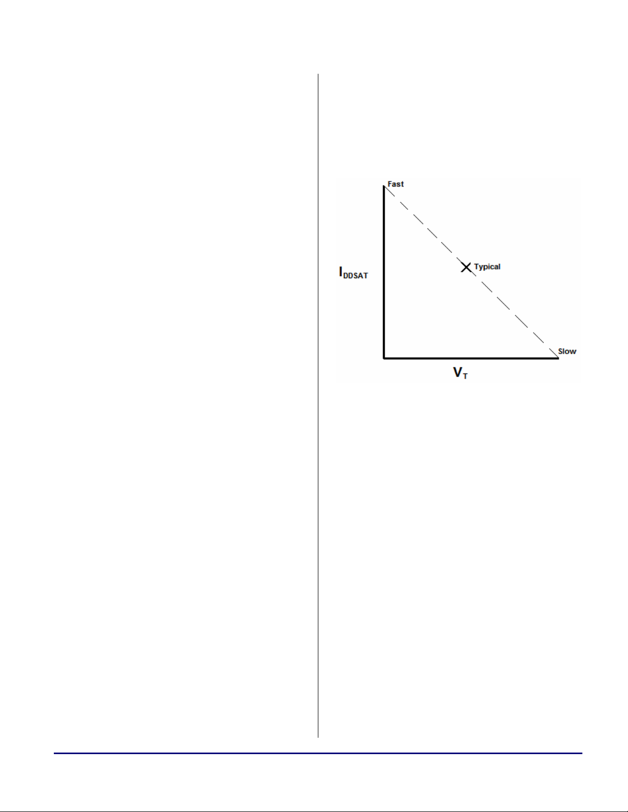
results in three process-related groupings. Figure
1 shows a process curve, which is a graphical
representation of this categorization based upon
transistor threshold voltage (
current (
I
DDSAT
).
V
) and saturation
T
which the part is expected to run. Leakage
current increases as temperature and/or voltage
increases.
The dynamic power component is largely
independent of temperature and is a function of
supply voltage and switching frequency. The
faster the transistors can switch, the more voltage
swings occur. The higher the supply voltage, the
larger the voltage swing between the on and off
transistor states. Thus, the dynamic component
will increase with voltage and/or frequency.
The second major consideration in estimating
average internal power is the type of application
code expected to run on the processor.
Specifications in the data sheet were obtained
while the processor ran a 75% Dual-MAC and
25% Dual-ALU algorithm, which was fetching
slowly changing data from L1 data memory. All
peripherals were disabled, but the core and L1
memory were running. To help the board
designer “size” the voltage regulators, power
numbers under full stress conditions are provided
in this document. These conditions include the
core running an algorithm consisting of 100%
Dual-MACs and more strenuous data-switching
Figure 1. Process Curve (I
DDSAT
vs VT)
The process contains three “corners”: fast,
typical, and slow. A “fast corner” part results
when the threshold voltage is minimized and the
saturation current is highest. Conversely, a “slow
corner” part has high threshold voltage and low
saturation current. Although “fast corner” parts
allow for higher operating frequencies, the tradeoff is higher leakage current and higher
dissipated power in general.
characteristics. This is discussed in more detail
in the “Estimating Average Static Power” section
of this document.
Finally, the actual power numbers can fluctuate
within a defined range based on the processor
fabrication process at the transistor geometries
required for such high speeds. This is largely due
to the semiconductor doping process (i.e., ion
implantation), which does not result in uniform
connectivity among the transistors, yielding
slight variations of the die in any given wafer of
silicon. Other physical phenomena related to the
fabrication process also contribute to this non-
Estimating Average Static Power
The static component for average internal power
is a result of the leakage current that occurs even
when the transistors are not changing state.
When the clocks (core and system) are off and
voltage is applied to the core and L1 memory,
Blackfin processors are in “Deep Sleep” mode.
The data sheet shows the
I
DDDEEPSLEEP
measurement
to indicate the static current component that
contributes to the internal static power
consumption (
P
P = V * I
DDINT_ST DDINT DDDEEPSLEEP
DDINT_ST
):
uniformity. These physical differences cause
Estimating Power for ADSP-BF533 Blackfin® Processors (EE-229) Page 2 of 10
Page 3
a
Table 1 shows the “Internal Power Dissipation”
table from the ADSP-BF531/BF532/BF533
Blackfin Embedded Processor Data Sheet [1].
This table contains average internal current draw
measurements, which were taken from a
representative sample of typical parts. In terms of
the static current component,
I
DDDEEPSLEEP
, the
ambient temperature that yielded these numbers
was 25
°C, denoted by footnote 2. The table
shows that the drawn current increases when the
voltage rises from 0.8V to 1.2V. Although no
direct correlation between voltage increases and
leakage can be made, the table sufficiently
details the leakage that can be expected within
the acceptable voltage range at 25
°C for “typical
corner” parts.
internal power dissipated when the core is
running a 100% Dual-MAC algorithm, which
maximizes the workload on the core but is not
typical application code.
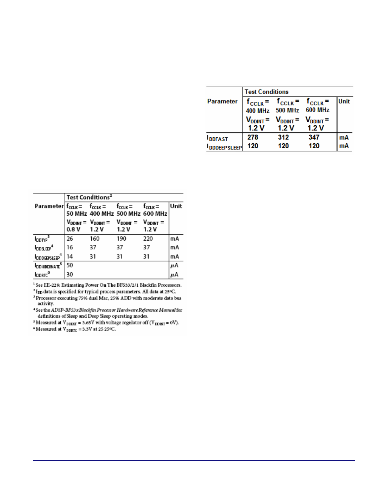
Table 2. Average I
on Faster Part (1.2V)
DDINT
The average internal power
!
consumption data is an average
measurement of the representative
sample of faster, higher leakage parts.
Therefore, some parts from within this
sample yielded power measurements
that slightly exceed the estimations
presented in this document as “worstcase”.
As can be extrapolated in the comparison
between Table 1 and Table 2, leakage current
can increase in magnitude by a factor of four due
to normal semiconductor processing variations.
Note that the current draw in Table 2 is labeled
I
to differentiate between the current draw
DDFAST
from typical parts (I
) and the current draw
DDTYP
obtained on faster, higher leakage parts.
Another important factor relative to leakage
Table 1. Internal Power Dissipation (Typical)
To help size the power supply, a set of faster,
higher leakage parts were measured. Table 2 is
similar to Table 1, except that it focuses on parts
that have higher leakage current, which are very
close to a worst-case average internal power
dissipation scenario in terms of silicon type with
no DMA and no peripherals enabled.
The ambient temperature is still 25
maximum 85
°C example is addressed in the
°C, as the
“Worst-Case Model” section of this note.
current is ambient temperature. Static power
consumption increases exponentially with
ambient temperature, as detailed by the equation:
P = P * e
DDINT_ST@T DDINT_ST@T0
where P
DDINT_ST@T0
is the power dissipated due to
leakage current at the known temperature (
P
and
DDINT_ST@T
temperature (
is the unknown number at the target
T). Using Table 2, the static
component of 120mA, given at
(0.015 * (T – T0))
T0)
T0 = 25°C, can be
multiplied by the supply voltage (1.2V) to obtain
the
P
DDINT_ST@T0
value of 144mW. Since the goal is
Additionally, these numbers reflect average
Estimating Power for ADSP-BF533 Blackfin® Processors (EE-229) Page 3 of 10
Page 4
a
to estimate the worst-case scenario in terms of
temperature, the target temperature
T is 85°C.
Given these known values, the estimate for
P
DDINT_ST@T
P
can now be calculated:
DDINT_ST@85°C
= 144mW * e
= 144mW * 2.4596
= 354.183mW
(0.015 * (85 – 25))
To compare to the values detailed in Table 2,
extract the current component:
I
DDDEEPSLEEP@85°C
= 354.183mW / 1.2V
= 295mA
= P
DDINT_ST@85°C
/ V
DDINT
The actual average measurement on a set of
faster parts under these conditions yielded:
I
DDDEEPSLEEP@85°C
= 302mA
As shown, the exponential estimate is within 3%
of the measured value. For those who do not
care for exponents, it is observed that the leakage
current roughly doubles for every 50
°C increase
in ambient temperature. In other words:
I
DDDEEPSLEEP@75°C
= 2 * I
= 2 * 120mA
= 240mA
DDDEEPSLEEP@25°C
Since the temperature increase from 25°C to
85
°C is greater than 50°C, the baseline for the
doubling leakage current changes from the
known value at 25°C to the estimated value at
75
°C. The same “doubles over 50°C” theory is
applied again, knowing that the increase is now
10°C instead of 50°C, which is 20% of the 50°C
used in the doubling estimation. Therefore, the
estimated leakage at 85
increase over the estimated leakage at 75
I
DDDEEPSLEEP@85°C
= 1.2 * I
= 1.2 * 240mA
= 288mA
°C is roughly a 20%
°C:
DDDEEPSLEEP@75°C
This method, while not as accurate as the
exponential estimate, is still within an error of
5% and is a fairly accurate mathematical model.
The “doubling” estimate is not linear, so the
error increases once the 20% assumption is
made.
In summary, these methods can be applied for
the acceptable ambient temperature range once a
baseline “Deep Sleep” mode current
measurement is obtained from the part in
question at the operating voltage of choice. Also,
please recall that these measurements and
estimations are averages across a representative
sample of parts.
Estimating Average Dynamic Power
The dynamic component of average internal
power is a function of the operating frequency
and the supplied voltage. Remember that the
values in Table 2 are from a set of faster, higherleakage parts and represent the maximum current
drawn at 1.2V and 25
°C on a fully-loaded core.
The process of extrapolating measurements by
virtue of frequency and voltage scaling will now
be discussed.
Table 2 shows the
frequencies with
I
measurements at three
DDFAST
V
= 1.2V. Using two
DDINT
measurements in the table, one can calculate the
ratio of current draw increase to frequency
increase. For example, the 400MHz
measurement for
I
DDFAST
is 278mA and the
500MHz measurement is 312mA. The ratio is
34mA per 100MHz, which can be seen between
500 and 600MHz as well. Once this ratio is
known, the expected current draw can be
calculated at any frequency:
I = I + [(F – F0) * Ratio]
DDINT@F DDINT@F0
where F is the target frequency, F0 is the known
frequency, and
Ratio is the change in current
draw per change in frequency. Given this model,
to estimate the total current drawn at 600MHz:
I = I + [(600 – 400) * (34/100)]
DDFAST600 DDFAST400
= 278 + 68
= 346mA
Comparing this estimated value with the
measured value at 600MHz (347mA), the
Estimating Power for ADSP-BF533 Blackfin® Processors (EE-229) Page 4 of 10
Page 5
a
estimate is within 1% of the actual data. In this
model,
Ratio is applied only as a dynamic
current adjustment to the total measured current
draw at a different frequency. Since the static
current component is independent of frequency
and is already included in the
I
DDFAST400
measurement, it is not impacted by this
adjustment.
A second extrapolation from the data in Table 2
is known as “frequency scaling”. A common
question regarding frequency scaling is “Why is
the current draw at 600MHz not equal to 1.5
times the value obtained at 400MHz?”. The basis
for this question is understandable because the
ratio from 400MHz to 600MHz is 1.5. However,
the answer is based on the fundamental
understanding that the static power component is
not affected by a change in frequency. In Table
2, the measured value
I
contains both the
DDFAST
static and dynamic components:
I
DDFAST600
= I
DDDEEPSLEEP
= 120 + 237
= 357mA
+ I
DD_DYN600
This estimate falls within an error of 3% of the
measured data of 347mA.
Aside from the frequency factor, the dynamic
component is also affected by changes in supply
voltage. Another extrapolation method called
“voltage scaling” can be applied to estimate
power when
V
is changing. Table 3 depicts
DDINT
the same data as Table 2, only now the supply
voltage has been increased 10% to the nominal
V
of 1.32V. The other parameters are the
DDINT
same (i.e., application is 100% Dual-MACs, and
ambient temperature is 25
°C):
I
where I
DDFAST
DDDEEPSLEEP
= I
DDDEEPSLEEP
is the leakage, which remains
+ I
DDFAST_DYN
constant across the frequency domain, and
I
DDFAST_DYN
is the dynamic component, which is
affected by changes in frequency. Since the
intent is to apply the dynamic power ratio to the
current draw measurement, the static component
must be removed prior to performing this
operation:
I
DDFAST_DYN400
= I
DDFAST400
= 278 – 120
= 158mA
- I
DDDEEPSLEEP
Because the frequency is being increased by a
factor of 50%, the dynamic ratio can be applied:
I
DD_DYN600
= 1.5 * I
= 1.5 * 158
= 237mA
DD_DYN400
At this point, the static component can be added
back in, yielding a total estimated current drawn:
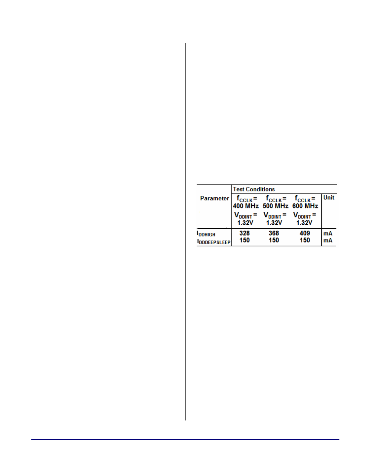
Table 3. Average I
on Faster Part (1.32V)
DDINT
Note that the nomenclature for the current draw
has changed to
I
to indicate that these
DDHIGH
numbers were obtained under the same
conditions as
of the highest allowed
I
, except now they are a result
DDFAST
V
. Using Tables 2 and
DDINT
3, one can obtain the two measurements taken at
400MHz for the typical current draw value:
I = 278mA
DDFAST400
I
DDHIGH400
= 328mA
Again, these numbers are a combination of the
static and dynamic components, so the static
component must be removed first:
I = 278 – 120 = 158mA
DDFAST400_DYN
I
DDHIGH400_DYN
= 328 – 150 = 178mA
The ratio of dynamic power consumption from
one applied voltage to another is directly
Estimating Power for ADSP-BF533 Blackfin® Processors (EE-229) Page 5 of 10
Page 6
a
proportional to the square of the voltage ratio
itself, or:
P
= (1.2V * 158mA) * (1.21)
DDHIGH_DYN
= P
DDFAST_DYN
= 229.416mW
* (1.32V/1.20V)
2
The current component is easily extracted by
dividing this value by the supply voltage:
I
= 229.416mW / 1.32V
= 173.8mA
DDHIGH_DYN
= P
DDHIGH_DYN
/ 1.32V
Now the static component at 1.32V can be
added:
I
= I
DDHIGH
= 173.8 + 150
= 323.8mA
DDHIGH_DYN
+ I
DDHIGH_DEEPSLEEP
The estimated value is within 2% of the actual
value of 328mA. The total current draw can then
be used to calculate the average internal power
consumption:
P
= I
DDHIGH
DDHIGH
= 323.8mA * 1.32V
= 427.4mW
* V
DDINT
These extrapolation methods can be taken a step
further by applying both the frequency and
voltage scales with one equation. Since the
frequency ratio is linear, it can be factored into
the equation used for voltage scaling:
P
DDDYN@V
= P
* (V/V0)2 * (F/F0)
DDDYN@V0
Second, the known values are substituted into the
equation:
P
P
= P
DDDYN@V
DDHIGH_DYN
* (V/V0)2 * (F/F0)
DDDYN@V0
= P
DDFAST_DYN
= (1.2V * 158mA) * 1.815
= 344.124mW
* (1.32/1.2)2 * (600/400)
The current component is easily extracted by
dividing this value by the supply voltage:
I
= 344.124mW / 1.32V
= 260.7mA
DDHIGH_DYN
= P
DDHIGH_DYN
/ 1.32V
Now the static component at 1.32V can be
added:
I
= I
DDHIGH
= 260.7 + 150
= 410.7mA
DDHIGH_DYN
+ I
DDHIGH_DEEPSLEEP
The estimated value is within 0.5% of the actual
measured value of 409mA. The value can then be
used to calculate the average internal power
consumption:
P
= I
DDHIGH
DDHIGH
= 410.7mA * 1.32V
= 542.1mW
* V
DDINT
In summary, there are many methods available to
estimate internal power consumption based on
the values presented in the data sheet or on
values obtained under nominal conditions when
considering worst-case operating conditions.
where V0 is the reference voltage, V is the target
voltage,
F0 is the reference frequency, and F is
the target frequency. For example, the current
values in Table 2 at
F0=400MHz and V0=1.2V are
known and the wish is to obtain the estimated
measurements at
F=600MHz and V=1.32V. Again,
the first step is to remove the static component:
I
DDFAST400_DYN
= 278 – 120 = 158mA
Average External Power Consumption
Average external power dissipation is the
average power dissipated in the
V
DDEXT
power
domain. The number of components that
contribute to the overall external power value is
the number of enabled peripherals in a given
system. Each unique group of peripheral pins
contributes to a piece of the overall external
power based upon several parameters:
Estimating Power for ADSP-BF533 Blackfin® Processors (EE-229) Page 6 of 10
Page 7
a
• Number of output pins (O)
• Number of pins toggling each clock cycle (TR)
• Frequency at which the peripheral runs (
• Utilization factor - percentage of time that the
V
U)
DDEXT
)
peripheral is on (
• Load capacitance (C)
• Voltage swing (
f)
The equation used to derive each component’s
contribution to the total external power is:
P
DDEXT
= (V
)2 * C * f/2 * (O*TR) * U
DDEXT
The worst external pin power scenario is when
the load capacitor continuously charges and
discharges, requiring the pin to toggle
continuously. Since the state of the pin can
change only once per cycle, the maximum
toggling frequency is
power, the worst-case
f/2. In terms of supply
V
value is 3.65V. Table
DDEXT
4 contains data for a realistic example of a PPI
application, which runs several peripherals
simultaneously. Actual results may vary, but
again, the intent is to help designers size the
power supplies.
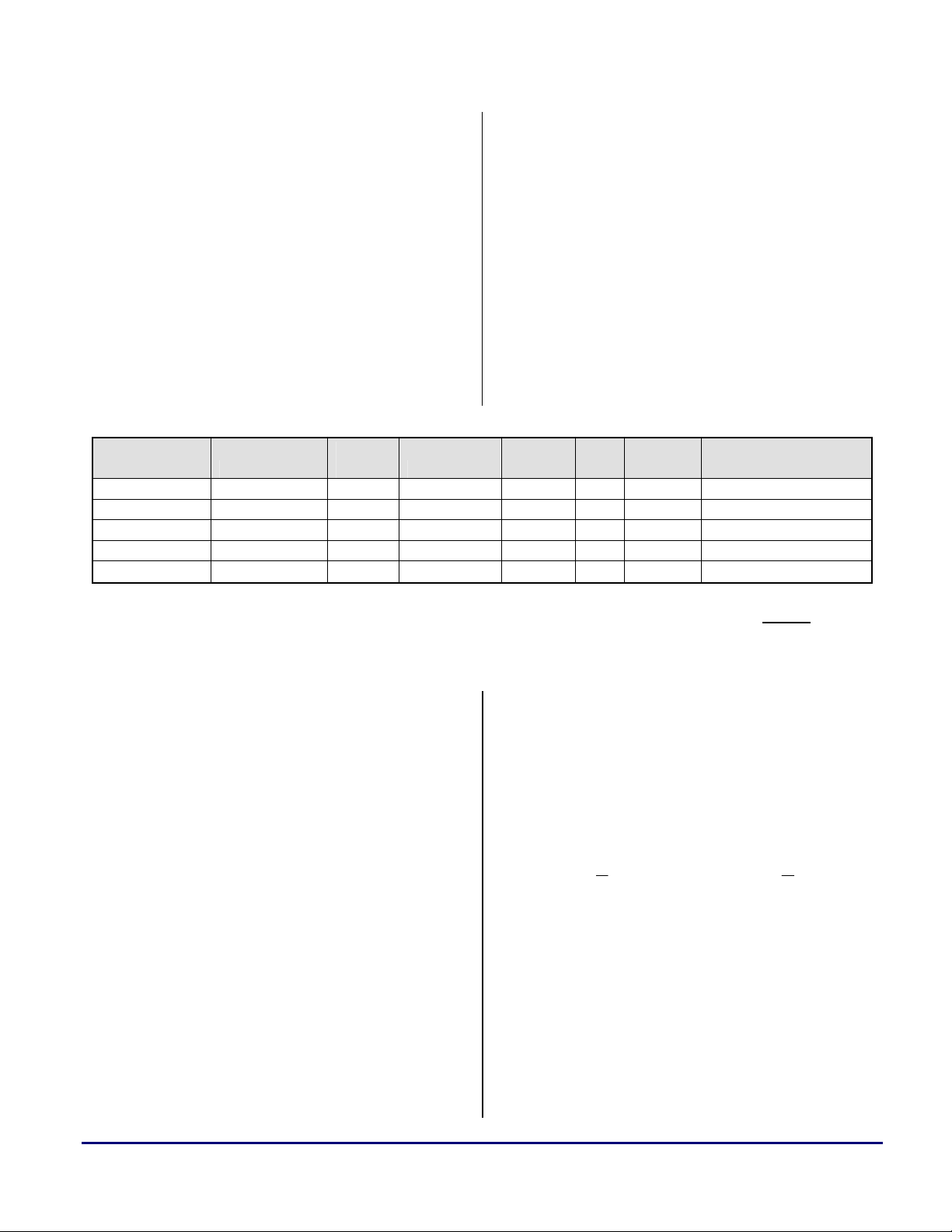
Peripheral Freq (Hz)
PPI 2.70E+07 9 3.00E-11 1 1.00 3.65 48.56
SPORT0 4.00E+06 2 3.00E-11 1 1.00 3.65 1.60
SPORT1 4.00E+06 2 3.00E-11 1 1.00 3.65 1.60
UART 1.15E+05 2 3.00E-11 1 0.25 3.65 0.01
SDRAM 1.33E+08 36 3.00E-11 0.25 0.50 3.65 119.60
Total External Power Dissipation @ 3.65V (est mW)
# of
pins C/pin (F)
Toggle
Ratio Util
Vddext
(V) Pout @ 3.65V (mW)
171.37
Table 4. Sample Calculation For Total Average External Power
In the above example, the total average external
power consumption is estimated to be ~170mW.
This number was obtained with the parameters
listed in Table 4 by applying the
P
DDEXT
equation
given above. Notice that the recommended load
capacitance of 30pF when the
V
is 3.65V was
DDEXT
used in this calculation. The chosen operating
frequencies are reasonable for each of the
their application, adding or deleting rows as
necessary. Since the equation provides results in
Watts (W), an additional scale factor of 1000 in
the spreadsheet converts results into mW.
This second equation is a more theoretically
accurate version of the one used in the
spreadsheet:
peripherals, including the maximum allowed
SDRAM frequency of 133MHz. This model
assumes that each output pin changes state every
clock cycle, which is a worst-case model, except
in the case of the SDRAM (because the number
of output pins transitioning each clock cycle will
be less than the maximum number of output
pins). Table 4 was taken from External Power
Spreadsheet [2], which is associated with this
EE-Note. It contains calculations for four sample
systems. The reader can tailor this spreadsheet to
Rather than estimating average external power
dissipated in each peripheral, the estimate
applies to each individual output pin, based on
the pin’s load capacitance and average toggling
frequency. The voltage swing is uniform across
all output pins within the
it is multiplied by the summation of the dynamic
charge changes on each output.
ext
2
V
DDEXT
⋅⋅=
∑
fCVP
LDDext
−−
PinsOutputAll
supply domain, so
Estimating Power for ADSP-BF533 Blackfin® Processors (EE-229) Page 7 of 10
Page 8

a
Using the PPI data in Table 4, nine output pins
change every cycle at an average frequency of
27MHz. Since toggling between on-to-off and
off-to-on requires two cycles,
F
is half the PPI
AVG
clock (13.5MHz). Since each pin changes at the
same rate and the pin capacitance is, presumably,
the same, the summation is simply nine times the
value of any one PPI pin:
P
= V
EXT_AVG
= (3.65)
= 13.3225 * 0.003645
= 0.048561W
= 48.561mW
2
* 9 pins * (F
DDEXT
2
* 9 * 13.5e6 * 30e-12
* CL)
AVG
As can be seen, the value derived using this
equation is the same as the value estimated in
Table 4. This model obtains the same estimate on
a per-pin basis rather than a per-peripheral basis.
Finally, a board designer must also be mindful of
power supply efficiency when sizing the
V
DDEXT
supply. Refer to Switching Regulator Design
Considerations for ADSP-BF533 Blackfin
Processors (EE-228) [3] for more details
regarding the Internal Voltage Regulator.
modes. Having a battery supply the
allows the removal of the
V
V
and V
DDINT
DDRTC
domain
DDEXT
supplies, thus significantly reducing total average
power consumption.
Worst-Case Model
To help size voltage regulators, let’s consider the
worst-case conditions under which an ADSPBF533 processor might operate (maximum
supply voltage, maximum ambient temperature,
and maximum operating frequency). To further
stress the part, a full load of 100% Dual-MAC
operations would be performed by the core and
the part under scrutiny would be the faster,
higher leakage type. Table 3 shows the current
drawn with all of the parameters maximized
except the ambient temperature. Table 5 contains
the same measurements taken at the maximum
ambient temperature, 85
°C.
Real-Time Clock (RTC) Power Consumption
The final source of total power consumption
comes from the optional third power domain, the
Real-Time Clock power domain (
V
DDRTC
), which is
a specified value. The RTC can be powered
between 2.25V and 3.6V. For a worst-case
analysis, a supply voltage of 3.65V yields a
current draw of 30-50µA for a range of ambient
temperature from 25
°C to 85°C. For the sake of
including this number in the final “Worst-Case
Model”, the power consumption is:
Table 5. Maximum I
The current draw is now represented as
(Extreme Conditions)
DDINT
I
DDMAX
to
differentiate between the current measurements
under these extreme conditions versus those
obtained in previous data sets. These numbers do
not include DMA or peripheral activity, but it is
estimated that the internal power dissipation will
increase by a maximum of 10% with these
additional parameters. Characterization tests are
being conducted to identify what sort of power
P
DDRTCMAX
= V
= 3.65V * 50µA
= 182.5µW
DDRTCMAX
* I
DDRTCMAX
draw increase might be expected in the internal
power domain when peripherals are enabled, but
two stipulations exist that may deem these
increases negligible.
Knowing this value also helps in selecting a
battery as a potential power source for the RTC.
The RTC can be used to take the ADSP-BF533
First, the application being run to generate these
I
numbers is not realistic because it keeps a
DDMAX
processor out of any of the low-power operating
Estimating Power for ADSP-BF533 Blackfin® Processors (EE-229) Page 8 of 10
Page 9

a
full load on the core 100% of the time, which is
not indicative of a real application.
Second, peripheral hardware activity and DMA
will cause stalls in the code being executed by
the “fully-loaded” core, which will save power in
the core dissipation when small increases in
dissipation are being introduced elsewhere onchip. Given these facts, the measurements in
Table 5 should be considered as the worst-case
scenario.
From this data, the extreme worst case for total
power dissipation can be estimated, assuming all
the conditions in Table 5 are met, for the
P
DDMAX
component. The external power component,
P
, is the example used in the “Average
DDEXT
External Power Consumption” section of this
document and the Real-Time Clock component
implies a maximum
temperature of 85
°C.
V
of 3.65V and ambient
DDRTC
The ADSP-BF533 is available in two
!
speed grades, 500MHz and 600MHz.
Although the 500MHz part can be run
up to 85
specified up to 70
°C, the 600MHz part is
°C. Therefore, the
“worst-case” conditions vary between
the two.
Using the data in Table 5 and given all of these
assumptions, the total power dissipation,
P
DDTOT
,
can be estimated for the 500MHz part:
P
= P
DDTOT500
= (579mA*1.32V) + 171.37mW + 182.5µW
= (764.28 + 171.37 + 0.1825)mW
= ~936mW
DDMAX500
+ P
DDEXT
+ P
DDRTC
For the 600MHz part, the measured current
drawn at 85
°C includes a leakage component of
362mA. Since the dynamic power component
remains the same across the temperature domain,
it can be separated out:
I = I - I
DDMAX_DYN600 DDMAX600 DDDEEPSLEEP
= 623 – 362
= 261mA
The static power component can then be used
with the exponential temperature model from the
“Estimating Average Static Power” section to
estimate the leakage at 70
P = P * e
DDMAX_ST@70°C DDMAX_ST@85°C
= (362mA * 1.32V) * e
= 477.84mW * 0.7985
= 381.563mW
°C:
(0.015 * (T – T0))
(–0.225)
The current component is easily extracted by
dividing this value by the supply voltage:
I = P / V
DDDEEPSLEEP@70°C DDMAX_ST@70°C DDINT
= 381.563mW / 1.32V
= 289.063mA
Now that both the static and dynamic current
components are known, a total current draw can
be calculated and used to estimate total average
power:
P = (I + I ) * V
DDMAX600 DDDEEPSLEEP@70°C DDMAX_DYN600 DDINT
= (289.063 + 261)mA * 1.32V
The total power dissipation, P
= 550.063mA * 1.32V
= 726.083mW
, can now be
DDTOT
estimated for the 600MHz part:
P = P + P + P
= 726.1mW + 171.4mW + 182.5µW
= (726.1 + 171.4 + 0.2)mW
= ~898mW
DDTOT600 DDMAX600 DDEXT DDRTC
These numbers are certainly not typical power
consumption numbers. Rather, they may occur if
all the critical parameters are maximized, the
application code fully stresses the core, and the
part is the faster, higher-leakage variety. These
numbers are being supplied to aid in specifying
the maximum power requirements for a
particular system’s voltage regulator.
Estimating Power for ADSP-BF533 Blackfin® Processors (EE-229) Page 9 of 10
Page 10

a
Conclusions
Several variables affect the power requirements
of an embedded system. Measurements
published in the ADSP-BF533 data sheet are
indicative of typical parts running under typical
conditions. However, these numbers do not
necessarily reflect the actual numbers that may
occur for a given processor under non-typical
conditions. The fabrication process plays a large
role in the total estimated power calculations that
are feasible for the ADSP-BF533. In addition to
the type of silicon that the customer could have,
the ambient temperature, core and system
frequencies, supply voltages, pin capacitances,
power modes used, application code, and
peripheral utilization all contribute to the average
total power that may be dissipated.
Even with all the estimates discussed in this
document, the result is an estimated average
power consumption number at any given time.
Assuming that a system can be in several
possible states, calculating a true average power
dissipation, the user would be required to run a
statistical analysis to determine what percentage
of the time the processor spends in each of the
defined states, apply those percentages to the
estimated power consumption calculated for that
state, and then add each of the state averages. For
example:
STATE1 = 20% of application
STATE2 = 10% of application
STATE3 = 70% of application
For example, if statistical analysis yields the
numbers above for percentage of time spent in a
particular system state, the total average power
(
P
) is summarized as follows:
TOT
P
= (0.2*P
TOT
STATE1)
+ (0.1*P
STATE2
)+ (0.7*P
STATE3
)
The average power number that results from this
equation shows how much the Blackfin
processor is loading a power source over time.
Do not use this calculation to size the power
supply! The power supply must support peak
requirements.
Average power estimates are useful in terms of
expected power dissipation within a system, but
designs must support the worst conditions under
which the application can be run.
References
[1] ADSP-BF531/ADSP-BF532/ADSP-BF533 Blackfin Embedded Processor Preliminary Data Sheet. Rev. PrC,
January 2004. Analog Devices, Inc
[2] External Power Spreadsheet. Associated file with Estimating Power for ADSP-BF533 Blackfin Processors (EE-229)
February 2004. Analog Devices, Inc.
[3] Switching Regulator Design Considerations for ADSP-BF533 Blackfin Processors (EE-228). Rev 1,
Available March 2004. Analog Devices, Inc.
Document History
Revision Description
Rev 1 – February 20, 2004
by Joe B.
Estimating Power for ADSP-BF533 Blackfin® Processors (EE-229) Page 10 of 10
Initial Release
 Loading...