

Page 1

Engineer-to-Engineer Note EE-226
a
Technical notes on using Analog Devices DSPs, processors and development tools
Contact our technical support at dsp.support@analog.com and at dsptools.support@analog.com
Or vi sit our o n-li ne r esou rces htt p:/ /www.analog.com/ee-notes and http://www.analog.com/processors
ADSP-2191 DSP Host Port Booting
Contributed by Michael Kuegler Rev 1 – January 23, 2004
1. Introduction
The Analog Devices ADSP-2191 DSP provides a
Host Port Interface (HPI) that can be used by a
Host to access the internal and external memory
and I/O space of the DSP via an 8- or 16-bit bus.
It is also possible to boot the DSP via the HPI
from the Host. The ADSP-2191 DSP is always
passive during Host Port accesses; therefore it is
called "Target" in this context. This application
note:
• Demonstrates how to access the Host Port
from an FPGA or PLD, using VHDL as the
design language.
• Provides an example of a software boot
loader, written in C, for booting the DSP via
the Host Port from a microcontroller or any
other processor.
and accesses the PLD using a set of low-level
interface functions (which have to be adapted to
the underlying hardware).
Screenshots from a logic analyzer, showing Host
Port transfers during the boot process, are found
in Chapter 7.
Chapter 2 outlines the HPI features and
configuration used in this design.
This document does not provide an
!
introduction to the Host Port, and it does
not explain all possible configuration
parameters.
A complete description of the HPI and
the Host Port I/O configuration registers
can be found in [1]. For detailed
information about pin-out and timing
requirements, refer to [2].
To achieve this, a test system has been designed
using another ADSP-2191 DSP as Host
processor and an Altera MAX7000 PLD between
the two DSPs.
The designed hardware is described in chapter 3.
Chapter 4 covers one of the two main objectives:
the VHDL design.
Chapter 5 describes the boot process and the boot
loader file, and Chapter 6 provides details about
the software boot loader.
Chapters 4 and 6 are independent of each other;
it is not necessary to know the internal function
of the PLD to use/understand the software boot
loader. The boot loader is written in generic C
Copyright 2004, Analog Devices, Inc. All rights reserved. Analog Devices assumes no responsibility for customer product design or the use or application of
customers’ products or for any infringements of patents or rights of others which may result from Analog Devices assistance. All trademarks and logos are property
of their respective holders. Information furnished by Analog Devices Applications and Development Tools Engineers is believed to be accurate and reliable, however
no responsibility is assumed by Analog Devices regarding technical accuracy and topicality of the content provided in Analog Devices’ Engineer-to-Engineer Notes.
!
2. Overview of Host Port
2.1. Pins
Table 1 lists the pins that make up the Host Port.
16 multiplexed address and data lines are
available for the HPI:
The source code for software boot
loader and VHDL design are not
included in this document; they may be
downloaded from the Analog Devices
Web site.
HAD[15..0].
Page 2
a
The default setting for the bus width after reset is
8 bits for data cycles, but the design described in
this note uses all 16 lines.
Address cycles always use the full bus
!
Two memory select lines provide the Host access
to internal and external memory (
I/O space (
The
Address Latch Enable (ALE) mode or Address
Cycle Control (ACC) mode. For ACC mode (as
used in this application), it must be driven high
during reset.
width (and
configured for 8 bits.
~HCIOMS).
HALE pin can be configured to function in
Pin Name Input/Output Pin Function
HAD[15..0] I/O/T Host Port Multiplexed Address and Data Bus
HA16 I Host Port Most Significant Address Line
~HCIOMS I Host Port I/O Space Select
~HCMS I Host Port Memory Select
HALE I Host Port Address Latch Strobe
~HWR I Host Port Write Strobe
~HRD I Host Port Read Strobe
HACK I/O Host Port Acknowledge
HACK_P I Host Port Acknowledge Polarity
HA16), even if the bus is
~HCMS) and
The polarity of the strobe signals
~HRD must also be configured. They are driven
high during reset, setting their active state low.
HACK and HACK_P determine the functionality
and polarity of the acknowledge signal during
reset.
Acknowledge mode (ACK) or Ready mode
(READY).
driven low during reset, setting up
ACK mode, active high.
!
HACK can be configured to act either in
HACK_P is driven high, and HACK is
HALE, ~HWR, ~HRD, HACK, and
HACK_P have to be driven during, and
for 10 peripheral clock cycles (HCLK)
after reset.
~HWR and
HACK in
Table 1. Host Port pins
2.2. Access Modes
Two modes provide the Host access to memory
and I/O space of the ADSP-2191 DSP: Direct
mode and DMA mode.
The Host boot loader (described in Chapter 6)
uses DMA transfers to write the content of the
loader file into the Target memory. Host Port
DMA behaves like any other DMA channel on
the ADSP-2191 DSP: the transfer direction can
be configured, Autobuffer and Descriptor mode
are available, and an interrupt can be generated
after completion of the data transfer. The
software boot loader uses Autobuffer DMA for
the boot process because it is suitable for
transferring large blocks of data without having
ADSP-2191 DSP Host Port Booting (EE-226) Page 2 of 25
to transmit the address for every word. The
disadvantage of DMA mode is that it has to be
configured, which requires several cycles. For
example, it takes five write accesses in Direct
mode from the Host to set up one Autobuffer
DMA transfer. If only one or two memory
locations need to be written to or read from,
Direct mode is more suitable. The Host boot
loader includes examples of read and write
accesses to internal memory and I/O space in
Direct mode, for which logic analyzer
screenshots are shown in Chapter 7.
Host Port DMA mode is available only
!
for accesses to memory, not I/O space.
Page 3
a
2.3. Host Port Registers
Several I/O configuration registers, as listed in
Table 2, are dedicated to the Host Port.
The Host Port Configuration Register, HPCR,
must be set up before any other access. It
contains configuration bits for various access
parameters, and some status bits, reflecting the
functionality of
signals sensed during reset.
For the chosen configuration (modes ACK and
ACC, low active strobe signals), the reset value
of HPCR is 0x0F00. To enable 16-bit bus width,
the value 0x0F01 is written into this register by
the Host after the Target has come out of reset.
Register Name
HACK and the polarity of control
DSP Address
Host Address
Before a read or write is done in Direct mode, the
data type (16- or 24-bit) and the memory page
should be set to the correct values by accessing
the Host Port Direct Page Register, HPPR.
Registers starting with HOSTD_ are used to
configure Host Port DMA transfers. Every DMA
transfer starts with the configuration of the
appropriate I/O registers (HOSTD_XXX); after
that, only data are transmitted or received – no
addresses need be written.
The access to I/O space registers is not
!
1
affected by the setting of HPPR.
Register Function
IOPG:Address
HPCR 0x07:0x001 0x1C01 Host Port Configuration
HPPR 0x07:0x002 0x1C02 Host Port Direct Page
HPDER 0x07:0x003 0x1C03 Host Port DMA Error
HPSMPHA 0x07:0x0FC 0x1CFC Host Port Semaphore A
HPSMPHB 0x07:0x0FD 0x1CFD Host Port Semaphore B
HPSMPHC 0x07:0x0FE 0x1CFE Host Port Semaphore C
HPSMPHD 0x07:0x0FF 0x1CFF Host Port Semaphore D
HOSTD_PTR 0x07:0x100 0x1D00 Host Port DMA Pointer
HOSTD_CFG 0x07:0x101 0x1D01 Host Port DMA Configuration
HOSTD_SRP 0x07:0x102 0x1D02 Host Port DMA Start Page
HOSTD_SRA 0x07:0x103 0x1D03 Host Port DMA Start Address
HOSTD_CNT 0x07:0x104 0x1D04 Host Port DMA Word Count
HOSTD_CP 0x07:0x105 0x1D05 Host Port DMA Chain Pointer
HOSTD_CPR 0x07:0x106 0x1D06 Host Port DMA Chain Pointer
HOSTD_IRQ 0x07:0x107 0x1D07 Host Port DMA Interrupt
Table 2. Host Port configuration registers
1
These addresses are not identical to the values listed in Appendix B, Table B-1, in [1], since the required address generation
is done in the PLD (left shift of actual address by 1 bit for I/O access).
ADSP-2191 DSP Host Port Booting (EE-226) Page 3 of 25
Page 4
a
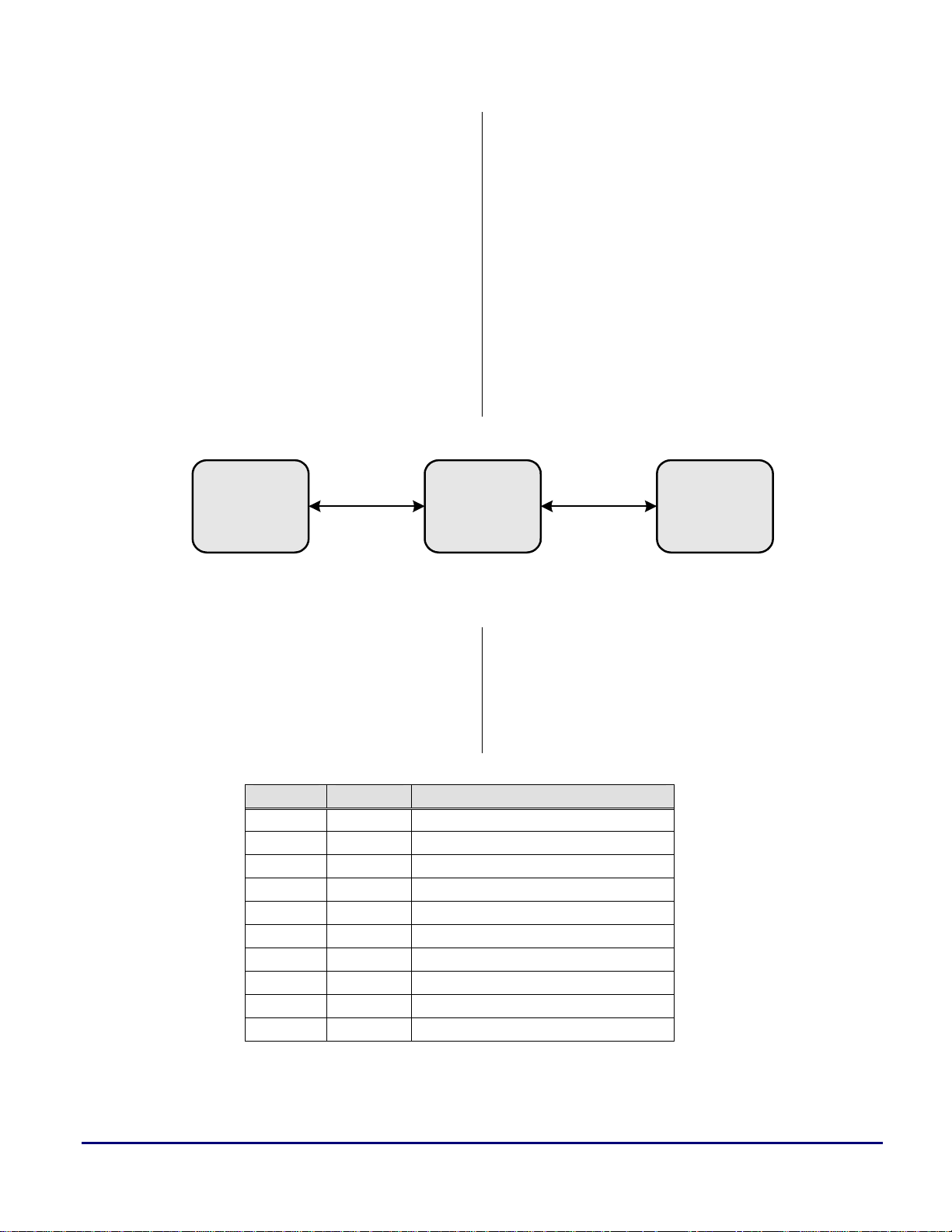
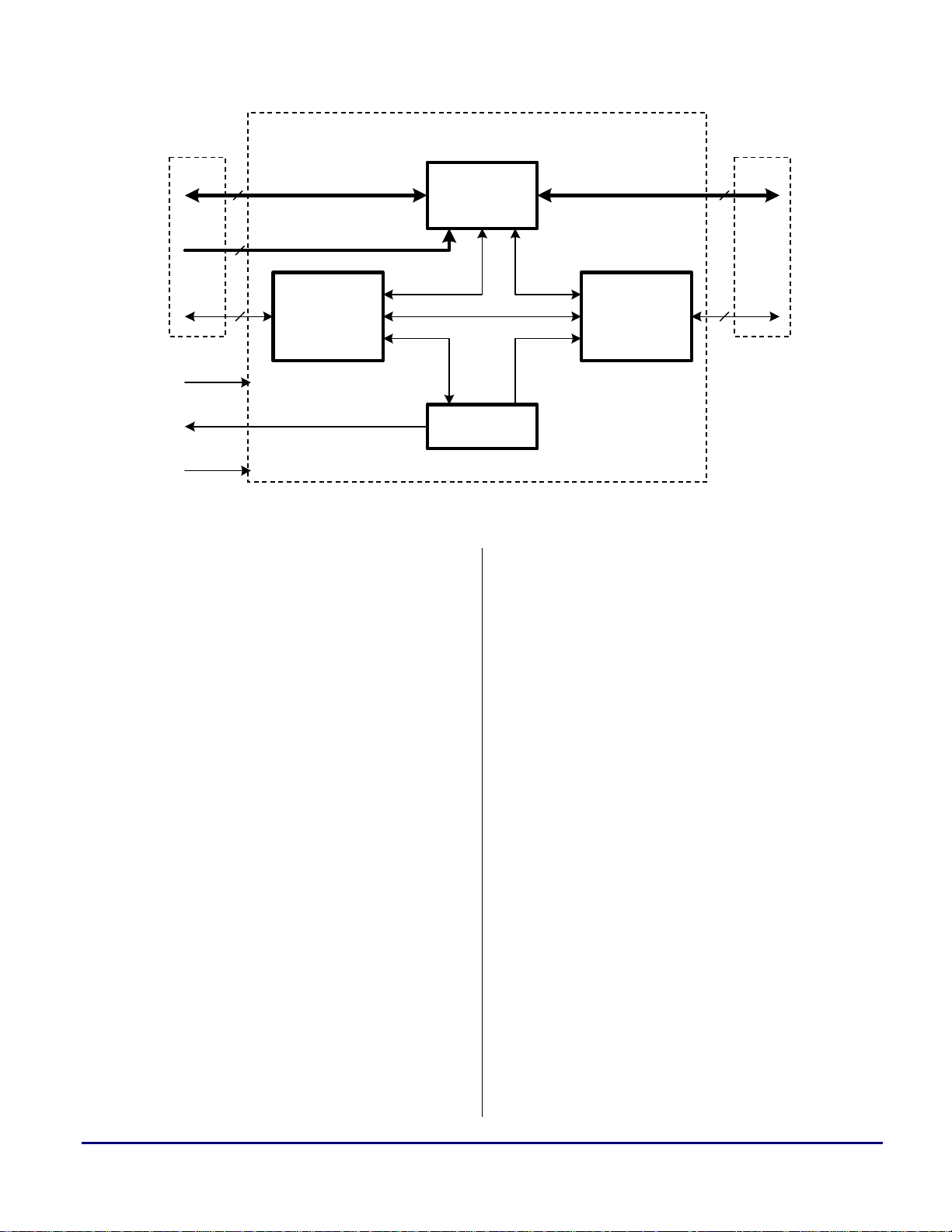
3. Hardware
The hardware used as the test platform consists
of a Host (ADSP-2191 DSP), a Target (ADSP2191 DSP), and an Altera PLD (see Figure 1).
The Host can be any kind of processor,
microcontroller, or other programmable device.
An ADSP-2191 DSP was chosen because it is
assumed that the reader is familiar with the
architecture of this DSP, so that there should be
no difficulty understanding the system on the
Host side.
Two ADSP-2191 EZ-KIT Lite™ boards serve as
platforms for the Host and Target. The PLD
Host
(ADSP-2191)
External
Port
PLD
(Altera)
resides on a customized PCB. Figure 2 shows the
connection of the three boards; the schematic
diagram can be found in Appendix A.
The External Port on the Host is connected to the
Host Port on the Target through a PLD. Besides
the two interfaces, two additional signals are
required: an error signal from the PLD to the
Host, and a reset signal controlled by the Host.
This reset signal is connected to the voltage
supervisor circuit on the Target board and the
PLD. It allows the simultaneous reset of Target
DSP and PLD.
Host
Port
Target
(ADSP-2191)
Figure 1. System overview
The loader file, which is transferred to the Target
by the software boot loader, is stored in the onboard Flash on the Host EZ-KIT Lite.
Two sets of jumpers, which are not shown in
Figure 2, configure the system:
Jumper Position Function
J1 1-2* Mode for HACK; default is ACK
2-3 (see ADSP-2191 HRM for details)
J2 1-2* ~HRD is low active
2-3 ~HRD is high active
J3 1-2* ~HWR is low active
2-3 ~HWR is high active
J4 1-2 HACK is low active
2-3* HACK is high active
J5 1-2* HALE acts in ACC mode
2-3 HALE acts in HALE mode
* default setting
On the Target EZ-KIT Lite board, Pins
OPMODE, BMODE0 and BMODE1 have to be
set to Host booting, as described in [4].
Table 3. Jumper settings for Host Port configuration
ADSP-2191 DSP Host Port Booting (EE-226) Page 4 of 25
Page 5
a
Five jumpers on the customized PCB configure
the Host Port, overriding the settings on the
Target board (smaller resistor values). Do not
change the default values as shown in Table 3,
ADSP-2191 EZ-KIT Lite
PF1
Host
ADSP-2191
PF0
Flash
AT49BV040
Error
Address
Data
Control
Reset
1
4
16
4 7
since the PLD is designed to interact with the
Host Port in modes ACK and ACC, with low
active strobe signals.
PLD
EPM7256AETC
Clock
50 MHz
1
17
1
HAD
Control
Reset
Reset
ADSP-2191 EZ-KIT LiteCustom PCB
Target
ADSP-2191
µP
Supervisor
Figure 2. Hardware block diagram
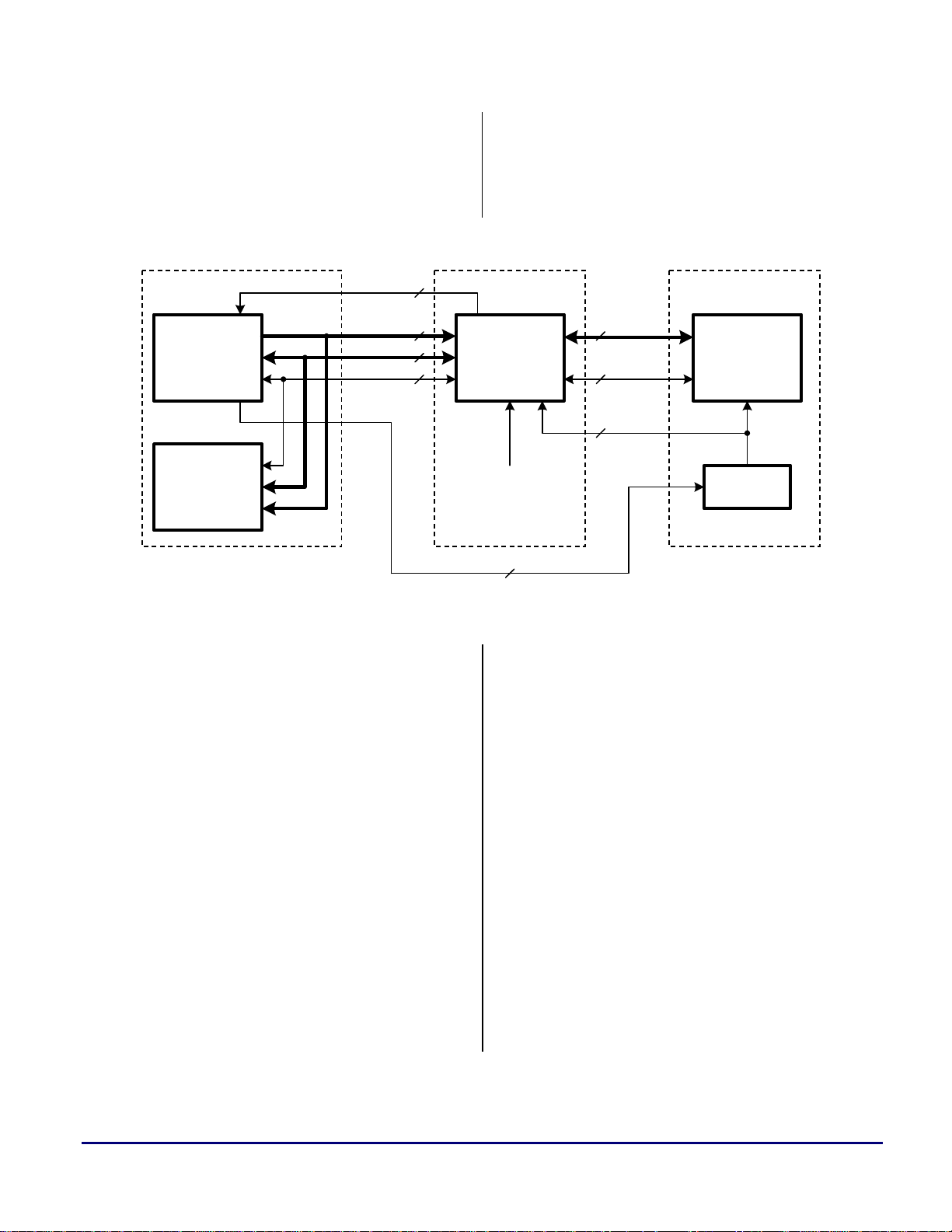
4. VHDL Design
4.1. Overview
Since the External Port on the Host and Host
Port on the Target are not completely compatible
with each other, additional logic is required. This
logic is implemented in an Altera MAX7000
PLD, which resides between Host and Target on
a customized PCB.
The design generates timing for Host Port modes
ACC and ACK.
The main building blocks of the VHDL design is
shown in Figure 3. A graphical representation of
the top-level design together with the pin
assignment is found in Appendix B.
All control signals of External Port and Host Port
are completely separated in the PLD. An access
from the Host is detected in block “External Port
interface logic”. This block will then signal to
the “Host Port interface logic” block that an
access to the Host Port has been requested.
No information is stored inside the PLD, so the
Host is held off until the access to the Target is
finished (flow-through system). This requires the
Host to wait for the PLD to acknowledge that the
access can be finished.
The data are transferred through block “Data
Path”, in which drivers are enabled/disabled
according to the direction of the data flow (read
or write).
The “Watchdog” block contains logic for error
detection.
ADSP-2191 DSP Host Port Booting (EE-226) Page 5 of 25
Page 6
a
To External
Port on Host
Data
16
4Address
Control
Reset
Error
Clock
Figure 3. PLD block diagram
4.2. Interface between Host Software and PLD
External Port
interface logic
Data Path
Watchdog
Data between the Host and the Target are
transmitted via a bi-directional, multiplexed
address and data bus. On the Host side, the data
bus of the External Port is used for this purpose.
All accesses to the Host Port can be considered
to be a (sequential) combination of address
cycles and/or data cycles. Information that
specifies whether an access is an address cycle or
data cycle, plus additional parameters are
encoded in four External Port address lines. This
method creates a “virtual address space”, which
means that there are no physical memory
locations implemented in the PLD. Rather, these
four address lines select the appropriate type of
access.
In summary, the virtual address space on the
Host side transfers information to help the PLD:
• Determine whether an address cycle or data
cycle is to be performed (addresses need to
be shifted on multiplexed address and data
bus due to byte addressing on Host Port)
• Select correct memory type for address
shifting (DM addresses need to be shifted left
To Host Port
on Target
Address
17
& Data
Control
Host Port
interface logic
64
by 1 bit; PM addresses need to be shifted left
by 2 bits)
• Assert appropriate chip select (
~HCIOMS)
~HCMS or
Table 4 shows the types of accesses that can be
performed through the PLD, and the addresses
that have to be used to trigger the access.
For example, a write to location 4 in the PLD
triggers a Host Port Address cycle, with the data
on the External Port data bus transferred to bus
HAD, shifted left by 1 bit, and with ~HCIOMS
asserted.
A read from location 1, on the other hand, starts
a Host Port Data read cycle, with
~HCMS
asserted, and no shifting of data on the
multiplexed bus.
One address location inside the PLD is dedicated
to a special purpose: A read from address 8
returns the revision number of the VHDL design.
Some addresses in the PLD are reserved, and
some combinations of access type and data
direction are invalid. A read from address 0, for
example, is not a valid Host Port access, since an
ADSP-2191 DSP Host Port Booting (EE-226) Page 6 of 25
Page 7
a
address read cycle is not specified for the Host
Port. When the Host performs an invalid access,
the PLD does not signal an error, but simply
PLD Address Access type Write / Read
0 DM Address W / 1 DM Data W / R
2 PM Address W / 3 PM Data W / R
4 IO Address W / 5 IO Data W / R
6 - 7 Reserved - / -
8 PLD Version - / R
9 - 15 Reserved - / -
Table 4. Virtual address space for performing different HPI accesses through the PLD
The External Port address lines are not
!
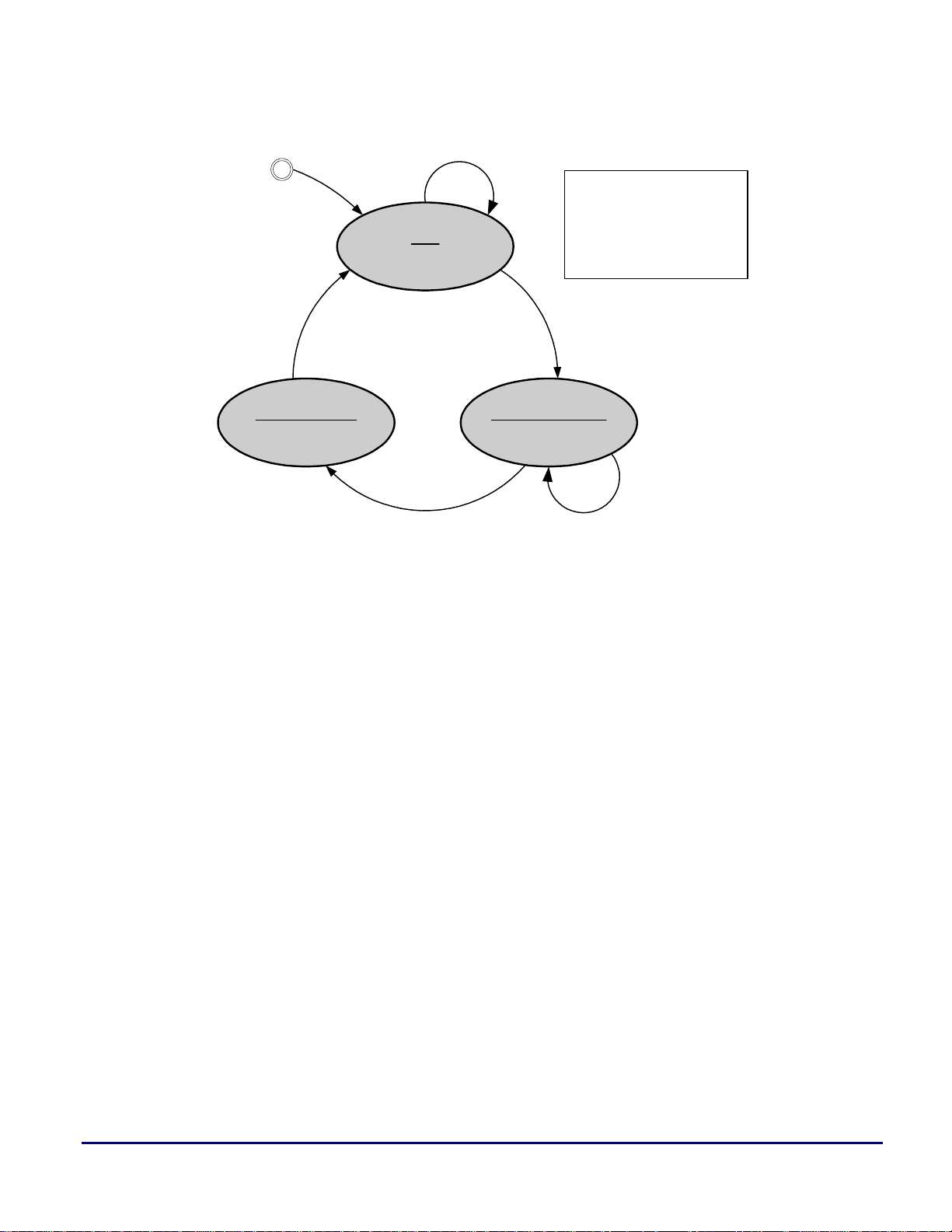
4.3. External Port Interface Logic
When the Host starts a read or write access to the
PLD, the External Port interface logic detects
this, and signals to the Host Port interface logic
to start a Host Port access. Some logic gates are
used to assert a signal when the Host begins an
access. This signal, in turn, starts a state machine
(Figure 4) that simply waits until one of the
following conditions is met:
• Host Port state machine finishes cycle
• Error signalled from Watchdog
• Invalid access signalled from Data Path
After that,
the end of the access.
used to transmit addresses to the PLD,
but carry additional information required
for the Host Port access.
ACK is asserted to the Host, marking
acknowledges the access. The data on the
External Port are not valid in such a case (PLD
bus drivers are tri-stated).
4.4. Host Port Interface Logic
This section describes the “core” of the VHDL
design: The logic required for driving the Host
Port control signals. It consists mainly of a state
machine used to generate the timing, as given in
[2]. The state diagram is given in Figure 5 on the
following page.
Access to the Host Port in Direct mode consists
of an address cycle and one or more data cycles.
In DMA mode, only data cycles are performed.
One complete execution of the state machine in
Figure 5 triggers one address cycle or one data
cycle, depending on the input values.
A complete Host Port access can be “assembled”
by executing the Host Port state machine several
times with the appropriate parameters.
For example, access to 24-bit Program Memory
with a 16-bit bus width in Direct Mode requires
one address cycle followed by two data cycles.
The state machine would be started three times in
this case: the first time configured for address
cycle, then two times with the input parameters
set to data cycle.
ADSP-2191 DSP Host Port Booting (EE-226) Page 7 of 25
Page 8
a
Reset
ACK_ASSERTED
ACK = 1
Figure 4. External Port state machine
i_start = 0
IDLE
ACK = 0
i_start
0: Start signal deas serted
1: Start signal as serted
i_finish_ep_access
0: Signal deasserted
1: Signal asserted
i_start = 1
WAIT_HP_ACCESS
_
i_finish_ep_access = 0i_finish_ep_access = 1
ADSP-2191 DSP Host Port Booting (EE-226) Page 8 of 25
Page 9

a
Reset
MEM_SEL_DEASSERTED
HCMS and HCIOMS = 1
o_sm_finished = 1
ADDR_LATCH_DEASSERTED
HALE = 1
i_host_cycle = 1
i_start = 0
IDLE
o_sm_finished = 0
i_host_cycle = 1
i_start = 1
MEM_SEL_ASSERTED
HCMS or HCIOMS = 0
i_host_cycle = 0
ADDR_LATCH_ASSERTED
HALE = 0
i_host_cycle = 0
STROBE_DEASSERTED
HWR and HRD = 1
WAIT_LATCH_HAD
o_latch_had = 0
i_hack = 1
i_host_strobe = 0
LATCH_HAD
o_latch_had = 1
&
WAIT_HACK
_
i_hack = 0
i_hack = 1
&
i_host_strobe = 1
STROBE_ASSERTED
HWR or HRD = 0
i_start
0: Start signal deas serted
1: Start signal as serted
i_host_cycle
0: HP address cycle
1: HP data cycle
i_host_strobe
0: HP write access
1: HP read access
i_ack
0: HACK deasserted
1: HACK asserted
Figure 5. Host port state machine
ADSP-2191 DSP Host Port Booting (EE-226) Page 9 of 25
Page 10
a
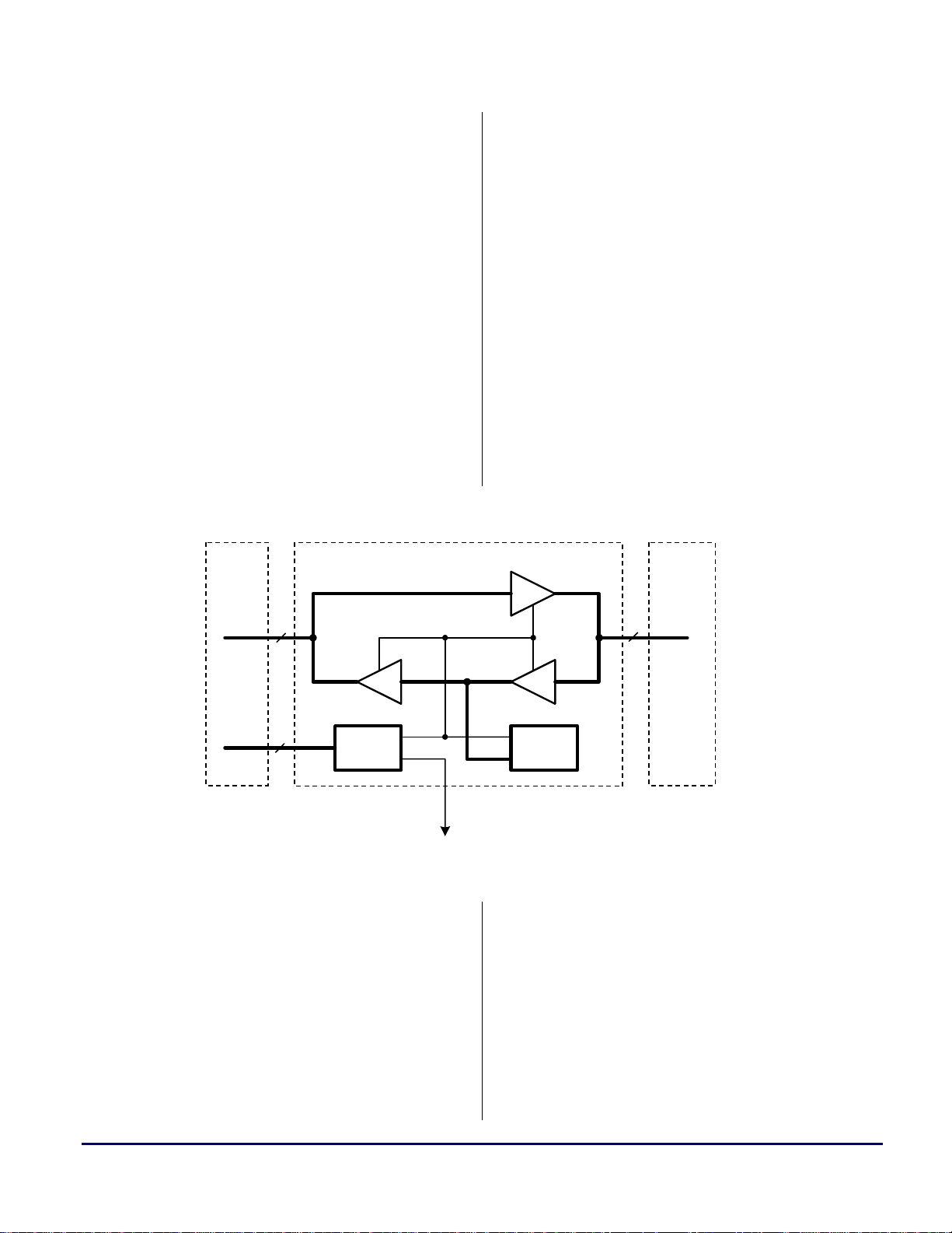
4.5. Data Path
The Data Path block accomplishes the bidirectional data transfer between Host and Target
via the multiplexed address and data bus.
The Host Port uses byte addressing, which means
that addresses for accesses to DM and I/O space
are shifted left by 1 bit, whereas addresses for
PM need to be shifted left by 2 bits. Address
generation is done in the Data Path block. The
details about the type of access (address cycle or
data cycle; access to memory or I/O space;
access to DM or PM) are decoded from
information contained in the External Port
address lines.
This block also detects whether the current
operation is a valid access. Due to the address
To External
Port on Host
mapping described earlier, invalid combinations
of access type and data direction can occur. For
example, the virtual address space allows an
address read cycle, which is not defined for the
Host Port. In such a case, the PLD acknowledges
the access to the Host without executing the
access to the Host Port. Accesses to reserved
addresses, or incorrect combinations of access
type and data direction, do not cause
ERROR to
be asserted. The Host is responsible for
performing valid operations only.
Figure 6 shows a simplified block diagram of the
Data Path. The shifters required to shift
addresses on the multiplexed address and data
bus are not shown.
To Host Port
on Target
Data
Address
Figure 6. Data path block diagram
4.6. Watchdog
16 17
4
Decoder
Valid Access
The Watchdog has two functions:
Should the Host not wait for an acknowledge
from the PLD, and start an access while the
previous access is still occurring, the Watchdog
detects this and signals an error to the Host. This
error is caused by an incorrect External Port
setup, which should be configured for “external
acknowledge only”.
Address
& Data
PLD
Version
The second, more important function of the
Watchdog, is to detect when the Target DSP
does not respond to a Host Port access with the
assertion of
ERROR signal is asserted to the Host.
the
HACK. After a certain length of time,
In both cases, the Watchdog resets the Host Port
state machine and forces the External Port state
machine to finish the access by asserting the
External Port acknowledge signal.
ADSP-2191 DSP Host Port Booting (EE-226) Page 10 of 25
Page 11

a
5. Booting via Host Port
5.1. Boot Mode Configuration
The ADSP-2191 DSP provides different means
of loading a program into memory, selected by
the state of three pins during hardware reset:
OPMODE, BMODE1, and BMODE0.
Driving
BMODE1 high during reset, causes the DSP to
start in Host boot mode. In this mode, the
processor simply waits in an endless-loop until a
‘1’ is written into the Host Port Semaphore A
register. Following this write, code execution
starts in internal memory at address 0x00 0000.
It is the Host’s responsibility to transfer all
program data into the Target memory before
writing to the semaphore register.
"
OPMODE and BMODE0 low, and
The last 16 locations in Program
Memory in Page 0 and the last 272
locations in Data Memory in Page 0 are
reserved and should not be used for the
placement of static data or code.
16 Bit
Control 1
Control 2
Flag
Address LSW
Address MSW
Count
Data 1
Data 2
:
Data N
Flag
Address LSW
Address MSW
Count
Data 1
Data 2
:
Data N
:
Figure 7. Format of 16-bit Host boot loader file
File Header
Block 1 Header
Block 1 Data
Block 2 Header
Block 2 Data
However, they can be used when the
boot process is finished.
5.2. Boot Loader File
For booting, VisualDSP++® provides a special
output file – the boot loader file. The default file
extension is ‘ldr’. Details about the creation of
the loader file and available options are
explained in [3].
Loader files can be created in 8- or 16-bit format.
The hardware described earlier uses 16-bit-wide
data buses, so the obvious choice is to create a
loader file that contains 16-bit data words. The
structure of a 16-bit Host boot loader file in
ASCII format is shown in Figure 7.
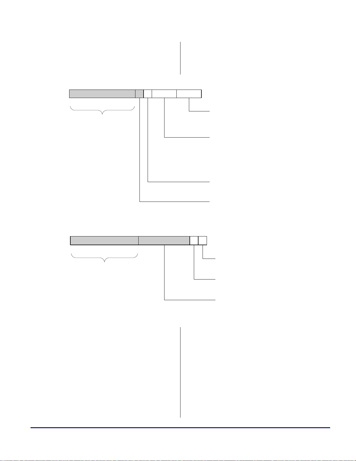
Control
The file begins with a file header, consisting of
two 8-bit control words (the upper 8 bits in both
words are not used and are padded with zeros).
The first word, Control 1, contains information
about the configuration of the External Port and
whether the Host should enable the SPI after the
boot process. A bit description for Control 1 is
given in Figure 8. Bit field Wait States holds the
number of wait states to be inserted for every
access to the External Port. The Base Clock
Divider determines the clock frequency for the
External Port. These two fields have meaning
only when code or data are to be placed in
external memory.
On the ADSP-2191 DSP, the SPIs are
multiplexed with SPORT2. Bit 6, OPMODE,
determines whether the SPIs or SPORT2 are
enabled. This bit corresponds to Bit 0 in the
System Configuration Register (SYSCR).
ADSP-2191 DSP Host Port Booting (EE-226) Page 11 of 25
Page 12
a
Only two bits are used in Control 2, the second
configuration word (see Figure 9). Bit 0, Host
Port Bus Width, determines whether the loader
file was created for 8- or 16-bit bus width (the
76543210
89101112131415
00000000
Unused
(padded with zeros)
Figure 8. Bit description of Control 1
00000000
word width of the values in the loader file). Bit 1,
CRC Checksum, indicates that a checksum is
used for the header file.
Wait States
000: 0 Wait states
: :
111: 7 Wait states
Base Clock Divider
000: HCLK / 1
001: HCLK / 2
010: HCLK / 4
011: HCLK / 8
100: HCLK / 16
101: HCLK / 32
OPMODE
0: 3 SPORTs selected
1: 2 SPORTs and 2 SPIs selected
Reserved
76543210
89101112131415
00000000
Unused
(padded with zeros)
Figure 9. Bit description of Control 2
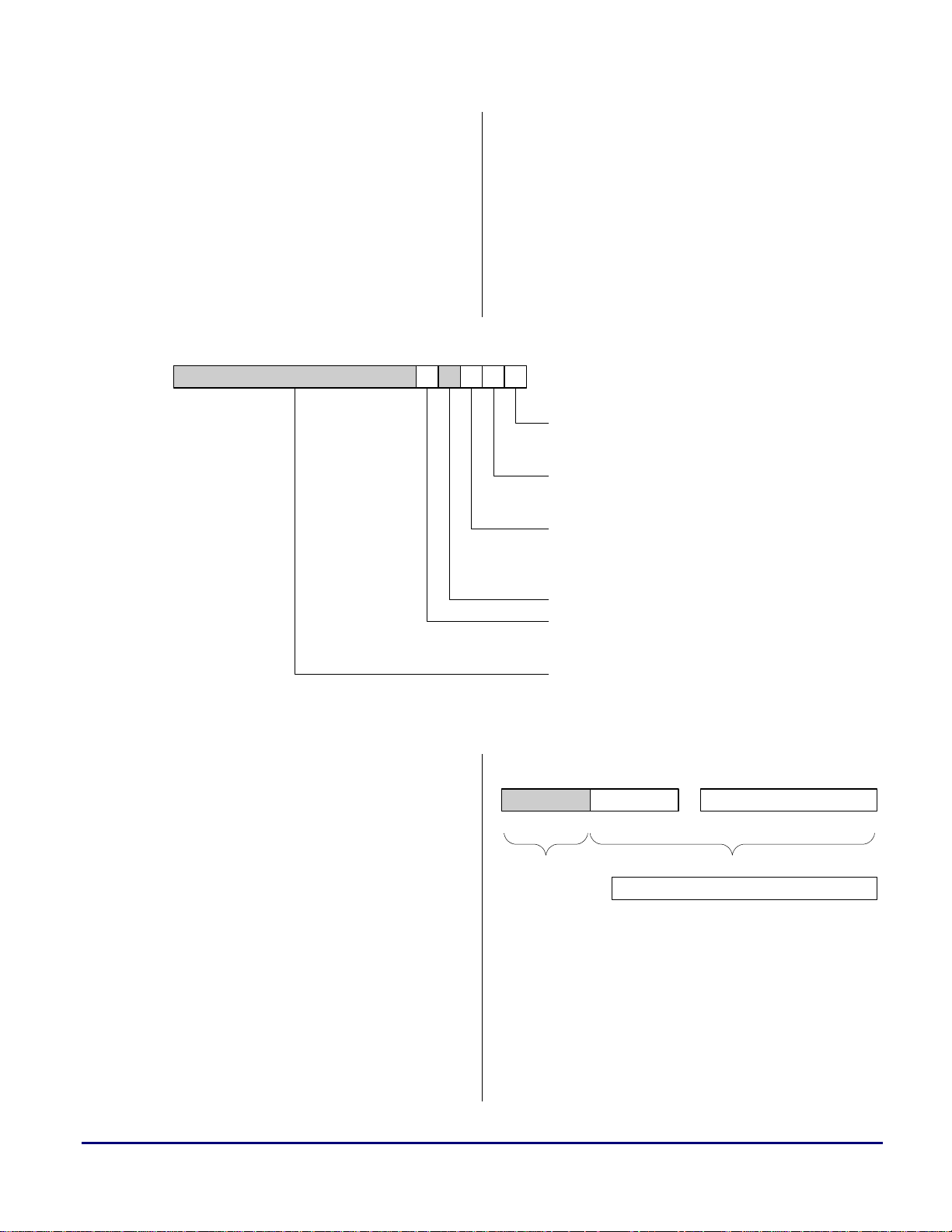
Flag
00000000
One or more block headers follow the file
header.
The first entry in every block header, called
Flag, is a 16-bit configuration word that contains
information about the payload following the
header. Figure 10 provides bit descriptions for
this configuration word.
Bit 0, Target Memory Type, specifies the width
of the values following the header or the values
Host Port Bus Width
0: 8 bit
1: 16 bit
CRC Checksum
0: Checksum not used
1: Checksum used
Reserved
the Host has to send to the Target to initialize a
part of memory to zero. A ‘0’ indicates access to
24-bit memory, and a ‘1’ indicates access to 16bit memory.
For the last header in the loader file, Bit 1, Final
Block, is set to ‘1’, indicating to the boot loader
that the end of the file has been reached.
If Bit 2, Zero-Init Memory, is cleared, the header
is followed by payload data. This block of data is
to be transferred to the Target DSP. If Bit 2 is
ADSP-2191 DSP Host Port Booting (EE-226) Page 12 of 25
Page 13
a
set, no data follow the header. Instead, the Host
initializes the specified memory block to zero.
This mechanism allows it to reduce the size of
the loader file, since there are often chunks of
memory containing zeros (for example external
and static variables in C programs are initialised
to zero by default if not otherwise initialised).
Bit 4 determines the External Memory Bus
Width. It is used only when data are to be placed
76543210
89101112131415
00000000
Figure 10. Bit description of Flag
00000000
in external memory. If this bit is set to ‘1’, the
bus width for the external port is 16 bits,
otherwise the bus width is 8 bits. The Host can
use this information to configure the external
port on the ADSP-2191 DSP. When a block
contains data for external memory, the Address
MSW field contains a non-zero value.
Target Memory Type
0: Program Memory (24 bit)
1: Data Memory (16 bit)
Final Block
0: More data follow after current block
1: Current block is the last in header file
Zero-Init Memory
0: Header is followed by data
1: Initialise memory to zero (no data
after header)
Reserved
External Memory Bus Width
0: 8 bit
1: 16 bit
Reserved
Address
The loader file described in this chapter contains
Address MSW Address LSW
70815 015
16-bit values. The address range of the ADSP2191 DSP, however, is 24 bits. Two 16-bit
values are necessary to provide a complete
address for the boot loader. The entries Address
MSW and Address LSW in the block header
Unused
(padded
with zeros)
023
Target memory address
provide that address. Address LSW contains the
16 least significant bits, and the lower 8 bits of
Address MSW contain the 8 most significant bits
Figure 11. Representation of Target memory address
in loader file
of the address in Target memory. The upper 8
bits of Address MSW are unused and always
Count
contain zeros. Figure 11 shows the representation
of addresses in the 16-bit loader file.
The last entry in every block header is Count,
which determines the number of data words for
the Target memory that follow the header (N), or
ADSP-2191 DSP Host Port Booting (EE-226) Page 13 of 25
Page 14

a
the number of words in Target memory that have
to be initialised to zero. If the Target Memory
Type in Flag was set to 16 bits, the number of
words following the header is N = Count. If
Target Memory Type was set to 24 bits, two data
words in the loader file are required to hold one
24-bit value. The number of 16-bit words
following the header is then N = 2*Count. In this
case, the 16 most significant bits of a 24-bit
value are stored in an even data word (Data 2n),
whereas the lower 8 bits of the 24-bit value are
stored in the upper 8 bits of an odd data word
(Data 2n-1). Figure 12 shows the packing of a
Loader file access
In file
“Loader File Access .c”
Figure 13. Software boot loader overview
Boot loader
“Boot Loader.c”
24-bit word into two 16-bit words in the loader
file.
Even data word (Data 2n) Odd data word (Data 2n-1)
023
24-bit word in Program Memory
n = 1, 2, … , N
Figure 12. Representation of 24-bit words in loader file
Host Port access
In file
In file
“Host Port Access.c”
70815 015
Unused
(padded
with zeros)
6. Software Boot Loader
General Description
A software boot loader, running on the Host
DSP, transfers the loader file to the Target DSP.
It reads the complete content of the loader file,
analyses the information in the headers, and
transfers the data contained in the file
accordingly via the Host Port to the Target
memory. Figure 13 shows a simplified block
diagram of the program.
Loader File Access
Access to the loader file is provided by the
following functions, which are stored in the file
“Loader File Access.c”:
• Open_Loader_File
• Close_Loader_File
• Read_Next_Loader_Value
For the system described earlier, where the
loader file is stored in Flash memory connected
to the Host, no “real” file handling is necessary.
Host Port Access
Data transfer to and from the Target Host Port is
handled by the following set of functions, located
in the file “Host Port Access.c”:
• Write_Target_IO_Direct
• Write_Target_DM_Direct
• Write_Target_PM_Direct
• Read_Target_IO_Direct
• Read_Target_DM_Direct
• Read_Target_PM_Direct
• Write_Target_DM_DMA
• Write_Target_PM_DMA
• Init_Target
A complete description of these functions can be
found in the source code.
A complete description of these functions can be
found in the source code.
ADSP-2191 DSP Host Port Booting (EE-226) Page 14 of 25
Page 15

a
For the current implementation, these functions
communicate with a PLD, which, in turn,
accesses the Host Port.
Boot Loader
The actual core of the boot loader, which is
located in the file “Boot Loader.c”, is written in
generic C, and can be executed on any platform
that supports this language. For this case, the
functions that access the loader file and Host Port
must be adapted to the underlying hardware. To
make porting the code to another platform easier,
the interface between boot loader and loader file
(and between boot loader and Host Port) are kept
in a very general form, so only the
implementation needs to be changed, not the
interface.
A flow chart of the software boot loader is
shown in Figure 14. After initializing the
hardware, the program sequentially reads the
values from the loader file. It uses the
information contained in the block headers to
initialize the Host Port DMA on the Target, and
then transmits the content of the data blocks into
the Target’s memory.
When the last block has been processed, writing
a ‘1’ into the Host Port Semaphore A register
starts program execution on the Target. The
transferred program is expected to write certain
values into pre-defined memory locations in
Program Memory and Data Memory. When the
Host finds the correct values in those handshake
locations, it is an indication that the boot process
was successful.
To ensure that the complete program has been
transferred correctly, the Host would have to
verify that every single word is correct in Target
memory. But the simple handshake just
described is considered to be sufficient for this
example project.
ADSP-2191 DSP Host Port Booting (EE-226) Page 15 of 25
Page 16

Start
Initialise External
Port on Host
Initialise PLD
Initialise Host
Port on Target
Read next header
from loader file
a
Clear handshake
locations in Target
PM and DM
Write ‘1’ to register
Semaphore A on
Target
Check handshake
locations in Target
PM and DM.
Configure Host
Port DMA on
Target
Transfer data from
loader file, or zero-
init memory on
Target
N
Figure 14. Boot loader flow chart
Last block
processed?
Y
7. Screenshots
This final chapter contains screenshots from a
logic analyzer showing the Host Port signals for
accesses to I/O space and memory in Direct
mode and DMA mode. The screenshots were
taken during different stages of the boot process.
Since the default Host Port bus width after reset
is 8 bits, the first action for the Host is to
End
Note: After writing a ' 1' i nto register
Semaphore A, program execution
starts on the Target. The prog ram
is expected to write handshake
values into defined m emory
locations in internal memory.
These values are read out by the
Host and indicate that the boot
process was successful.
configure the HPI for a 16-bit bus width. Bit 0 in
the Host Port Configuration Register must be set
to ‘1’ for that. Figure 15 shows the first access to
the Target after reset, consisting of two 8-bit
writes to HPCR (I/O address 0x3802). The reset
value of this register is 0x0F00, so the value
0x0F01 is written into it (first the LSB, 0x01;
then the MSB, 0x0F). After that, the Host Port is
configured for 16-bit bus width.
ADSP-2191 DSP Host Port Booting (EE-226) Page 16 of 25
Page 17
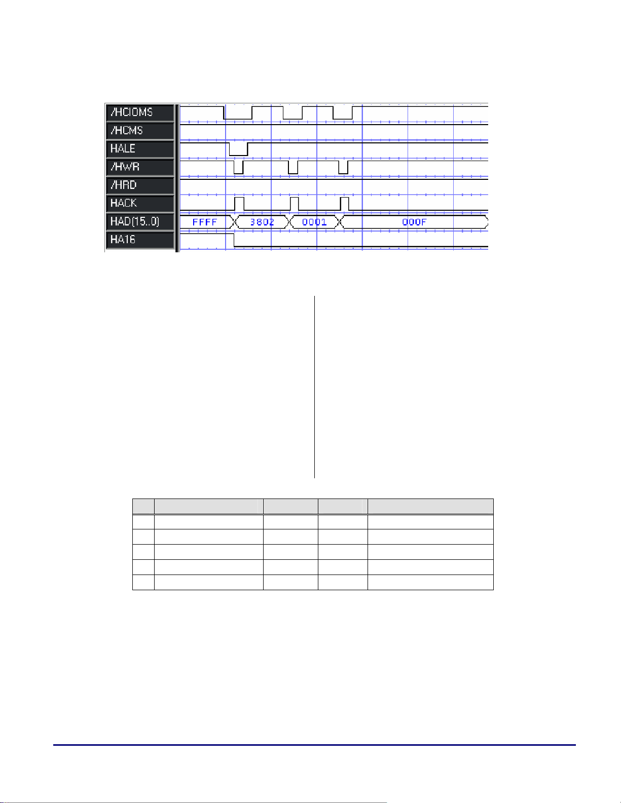
Figure 15. Direct write access to register HPCR in 8-bit mode
a
The software boot loader described earlier uses
Host Port Autobuffer DMA to transfer the data
segments stored in the loader file to the DSP. A
typical configuration for such a DMA transfer is
shown in Table 5, which contains the register
name to be configured, the address and value for
that register, and a short explanation of the
purpose.
The screenshot in Figure 16 shows the
corresponding transfers via the Host Port.
The DMA data transfer following the DMA
configuration is shown in Figure 17. The five
Transfer to register Address Value Comment
1 HOSTD_CFG 0x3A02 0x0010 Enable Autobuffer mode
2 HOSTD_SRP 0x3A04 0x0000 Set start page 0x00
3 HOSTD_SRA 0x3A06 0x8000 Set start address 0x8000
4 HOSTD_CNT 0x3A08 0x0005 Set word count 5
5 HOSTD_CFG 0x3A02 0x0017 Start DMA write
values being transmitted are 0x0061, 0x0064,
0x0069, 0x0000 and 0x8000; they will be stored
in five consecutive locations in DM, starting at
address 0x8000.
As can be seen, no addresses need to be sent
during DMA transfers. However, from the
amount of data necessary for a complete DMA
setup, it is obvious that using DMA is efficient
only for transferring large amounts of data, or
when the DMA configuration does not change.
Table 5. Example of Host Port DMA configuration
ADSP-2191 DSP Host Port Booting (EE-226) Page 17 of 25
Page 18

Figure 16. Configuration of Host Port Autobuffer DMA via Host Port
Figure 17. DMA write access of five 16-bit words
a
When the complete loader file has been
transferred to the DSP, writing a 1 into the
Semaphore A register starts program execution.
The screenshot in Figure 18 shows the value
0x0001 being written to address 0x39F8 (register
HPSMPHA), which marks the end of the boot
process.
Figure 19 shows a read from Data Memory
location 0xFFFF. The address is shifted left by 1
bit, and
from this location is 0x1234.
The transfer shown in Figure 20 is a 24-bit read
from Program Memory location 0x7FFF. The
HA16 is set to 1. The 16-bit value read
address is shifted left by 2 bits, and
to 1. The value read from this location is
0x123456.
The boot loader uses these last two reads as a
simple method for verifying that program
execution has started on the Target (the values
are written by the transferred program). When
the expected values can be found in the
handshake locations, it can be assumed that the
boot process was successful and the program is
running properly.
HA16 is set
ADSP-2191 DSP Host Port Booting (EE-226) Page 18 of 25
Page 19

Figure 18. Direct write access to register HPSMPHA (16-bit mode)
a
Figure 19. Direct read access from DM location 0xFFFF (16-bit data)
Figure 20. Direct read access from PM location 0x7FFF (24-bit data)
ADSP-2191 DSP Host Port Booting (EE-226) Page 19 of 25
Page 20

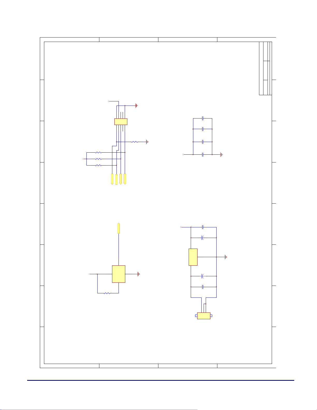
A. Schematic Diagram
D
C
B
A
a
8
7654321
CLOCK
TCK
TMS
TDI
Host 2191 PLD
Host 2191 PLD.Sch
TDO
13
Revision:
Sheet of
1 1.0
Time:
Host 2191 - Overview
19-Nov-2003 13:23:41
Host 2191 Overview.Sch
A4
Title
Size: Number:
Date:
File:
TDI
TCK
TMS
TDO
CLOCK
Host 2191 Miscellaneous
Host 2191 Miscellaneous.Sch
1 2 3 4 5 6 78
D
C
B
A
ADSP-2191 DSP Host Port Booting (EE-226) Page 20 of 25
Page 21

D
C
B
a
A
23
Revision:
Sheet of
1 1.0
Time:
Host 2191 - PLD
19-Nov-2003 13:24:03
Host 2191 PLD.Sch
A4
Title
Size: Number:
Date:
File:
VCC_3
HACK_P
+1+2+
J1
R2
8
Mode for HACK
(see ADSP-2191 HRM)
/HRD low active
/HRD high active
/HWR low active
/HWR high active
HACK low active
HACK high active
HALE in ACC mode
HALE in ALE mode
Jumper settings
1-2*
2-3
1-2*
2-3
1-2*
2-3
1-2
2-3*
1-2*
2-3
7654321
J1J2J3J4J5
Jumper Position Function
* default
Host Port Interface
TDI
TCK
TDO
TMS
TCK
TDO
73
62
IO62/TCLK
49
IO49
IO73/TDO
HA16
HAD0
HAD1
HAD2
HAD3
HAD4
53
57
52
50
54
56
IO53
IO57
IO5555IO52
IO50
IO54
IO56
VCC_3
Altera CPLD
TDI
TMS
4
15
IO4/TDI
VCCIO
VCCIO
VCCIO
VCCIO
VCCIO
VCCIO
VCCINT
VCCINT
IO15/TMS
82
66
51
34
18
3
91
39
/HRD
Shorting
Shorting
CON3
3
1k
(to Target)
P3
HAD5
HAD6
HAD7
HAD8
61
58
60
63
IO61
IO58
IO60
IO63
Jumper
HAD9
64
IO64
Jumper
+1+2+
J2
CON3
3
R3
1k
2
4
SCL
SDA
CLK26BD158BD1410BD1312BD1214BD1116BD10
5VDC1GND3CLK15AD157AD149AD1311AD1213AD1115AD1017AD919AD821AD723AD625AD527AD429AD331AD233AD135AD0
HAD11
HAD12
HAD13
HAD14
HAD15
HAD[15..0]
HAD10
HAD11
HAD12
HAD13
HAD14
HAD15
67
69
70
71
75
68
72
65
IO67
IO69
IO70
IO71
IO68
IO72
IO65
/HWR
+1+2+
J3
18
BD920BD822BD724BD626BD528BD430BD332BD234BD136BD0
HAD8
HAD9
HAD10
77
78
76
IO75
IO77
IO78
IO76
R4
HA16
HAD7
79
3
1k
HACK_P
HAD6
80
IO80
IO79
Shorting
CON3
HWR
HRD
HAD4
HAD5
81
83
IO81
IO83
Jumper
HACK
HALE
HAD2
HAD3
85
84
IO84
J4
HCMS
HAD1
ERRORHALE
92
IO85
HACK
+1+2+
R5
HCIOMS
38
37
HAD0
94
IO92
3
1k
IO94
IO9696IO9393IO98
GND
GND
GND
GND
GND
97
IO97
Shorting
CON3
IOMS
98
HALE
Jumper
+1+2+
J5
R6
43
42
41
40
39
MICTOR 19X2
WR
100
99
IO99
IO100
3
1k
GNDIO
GNDIO
GNDIO
GNDIO
GNDIO
GNDIO
GNDINT
GNDINT
Shorting
Jumper
CON3
Error signal from PLD to Host -
connect to PF1 on Host EZ-KIT
Reset from Target to PLD -
connect to Pin 7 (/RESET) of U15
(ADM708) on Target EZ-KIT
+
CON1
+
J7
CON1
1
RESET
J6
1
ERROR
95
74
59
43
26
11
86
38
U1
87
CLOCK
DATA14
DATA15
2
4
SCL
SDA
CLK26BD158BD1410BD1312BD1214BD1116BD10
(to Host)
5VDC1GND3CLK15AD157AD149AD1311AD1213AD1115AD1017AD919AD821AD723AD625AD527AD429AD331AD233AD135AD0
P1
External Memory Interface 1
D
IN/OE2/GCLK2
IN/GCLK1
90
CLOCK
DATA12
DATA13
89
RESET
DATA10
DATA11
18
IN/OE1
IO5
IO7
IO2
IO1
IO6
5
7
2
1
6
8
88
ACK
RD
DATA15
DATA14
DATA13
DATA12
DATA1
DATA2
DATA3
DATA4
DATA5
DATA6
DATA7
DATA8
DATA9
BD920BD822BD724BD626BD528BD430BD332BD234BD136BD0
ADDRESS1
ADDRESS2
ADDRESS3
IO9
IO8
IO1010IO14
9
DATA11
DATA10
DATA0
38
37
ADDRESS0
C
IO13
IO12
13
14
12
DATA9
DATA8
DATA7
DATA[15..0]
GND
GND
GND
GND
GND
IO17
IO20
IO16
17
20
19
16
DATA6
DATA5
DATA4
DATA3
43
42
41
40
39
MICTOR 19X2
IO2121IO19
DATA2
IO22
22
DATA1
IO23
24
23
DATA0
IO24
IO27
IO25
28
27
25
ADDRESS[3..0]
IO30
IO32
IO31
32
31
ADDRESS2
ADDRESS3
IO36
IO35
IO33
36
35
33
ADDRESS0
ADDRESS1
IO40
IO41
IO37
IO42
40
41
37
42
HWR
HCIOMS
IO28
IO29
30
29
(to Host)
P2
External Memory Interface 2
IO45
IO44
IO46
IO47
IO48
47
48
EPM7256AETC-100
WRRDACK
18
BD920BD822BD724BD626BD528BD430BD332BD234BD136BD0
45
44
46
HCMS
HRD
HACK
2
4
SCL
SDA
CLK26BD158BD1410BD1312BD1214BD1116BD10
5VDC1GND3CLK15AD157AD149AD1311AD1213AD1115AD1017AD919AD821AD723AD625AD527AD429AD331AD233AD135AD0
B
Note: An additional external connection is required:
PF0 on the Host EZ-KIT must be connected
to Pin 1 (/MR) of U15 (ADM708) on the
Target EZ-KIT.
IOMS
38
GND
43
GND
42
GND
41
GND
40
GND
39
37
MICTOR 19X2
A
1 2 3 4 5 6 78
IN/GCLR
ADSP-2191 DSP Host Port Booting (EE-226) Page 21 of 25
Page 22
D
C
B
a
A
8
Revision:
33
Sheet of
1 1.0
Time:
Host 2191 - Miscellaneous
19-Nov-2003 13:23:51
Host 2191 Miscellaneous.Sch
A4
Title
Size: Number:
Date:
File:
7654321
VCC_3
VCC_3
JTAG Interface
R9
10k
R8
10k
R7
10k
2
4
6
8
10
+
+
+
+
+
+
+
+
+
+
J8
HEADER 5X2
1
3
5
7
9
TCK
TDO
R10
10k
VCC_3
C8
100n
C7
100n
C6
100n
C5
100n
CPLD Decoupling - place close to device
TCK
TDO
TMS TMS
TDI TDI
TDI
TCK
TDO
TMS
D
VCC_3
Crystal Oscillator
C2
CLOCK
CLOCKCLOCK
8
OUT
VCC14GND
7
OE
OSC1
50 MHz
1
R1
10k
C
VCC_3
U2
Power Supply
100nF
10uF
C4
+
3
VOUT
GND
2
VIN
MIC29300
1
10uF
C3
+
C1
100nF
123
J9
B
POWER JACK
1 2 3 4 5 6 78
A
ADSP-2191 DSP Host Port Booting (EE-226) Page 22 of 25
Page 23

B. VHDL Top-Level Design
a
ADSP-2191 DSP Host Port Booting (EE-226) Page 23 of 25
Page 24

a
Pin Signal Pin Signal Pin Signal Pin Signal
1 ACK 26 GNDIO 51 VCCIO 76 2 ~RD 27 - 52 HA16 77 -
3 VCCIO 28 - 53 HAD0 78 4 TDI 29 - 54 HAD1 79 5 DATA15 30 - 55 HAD2 80 6 DATA14 31 ADDRESS3 56 HAD3 81 7 DATA13 32 ADDRESS2 57 HAD4 82 VCCIO
8 DATA12 33 ADDRESS1 58 HAD5 83 -
9 DATA11 34 VCCIO 59 GNDIO 84 10 DATA10 35 ADDRESS0 60 HAD6 85 11 GNDIO 36 - 61 HAD7 86 GNDINT
12 DATA9 37 - 62 TCK 87 CLOCK
13 DATA8 38 GNDINT 63 HAD8 88 GND
14 DATA7 39 VCCINT 64 HAD9 89 ~RESET
15 TMS 40 HALE 65 HAD10 90 GND
16 DATA6 41 ~HWR 66 VCCIO 91 VCCINT
17 DATA5 42 ~HCIOMS 67 HAD11 92 ERROR
18 VCCIO 43 GNDIO 68 HAD12 93 19 DATA4 44 ~HCMS 69 HAD13 94 20 DATA3 45 ~HRD 70 HAD14 95 GNDIO
21 DATA2 46 HACK 71 HAD15 96 22 DATA1 47 - 72 - 97 23 DATA0 48 - 73 TDO 98 ~IOMS
24 - 49 - 74 GNDIO 99 25 - 50 - 75 - 100 ~WR
Table 6. PLD Pin Assignment
ADSP-2191 DSP Host Port Booting (EE-226) Page 24 of 25
Page 25

a
References
[1] ADSP-219x/2191 DSP Hardware Reference. 2001. Analog Devices Inc.
[2] ADSP-2191M Data Sheet. 2002. Analog Devices Inc.
[3] VisualDSP++ Linker and Utilities Manual for ADSP-218x and ADSP-219x DSPs. 2002. Analog Devices Inc.
[4] ADSP-2191 EZ-KIT Lite Evaluation System Manual. 2001. Analog Devices Inc.
[5] Booting the ADSP-2191/95/96 DSPs (EE-131). April 2003. Analog Devices Inc.
[6] ADSP-2191 Host Port Interface (EE-154). October 2002. Analog Devices Inc.
Document History
Version Description
Rev 1 January 23, 2004
by M. Kuegler
Initial Release based on VisualDSP++ version 3.0
ADSP-2191 DSP Host Port Booting (EE-226) Page 25 of 25
 Loading...