

Page 1

Engineer To Engineer Note EE-165
Technical Notes on using Analog Devices' DSP components and development tools
=
The ADSP-2116x On-chip Sync Burst Controller
Contributed by R.Hoffmann April 30, 2002
When using a DSP to address SBSRAM, additional hardware will be needed to handle the synchronous
addressing mode. The ADSP-2116x family members ADSP-21160 and ADSP-21161 use a hardware
intensive solution, an on-chip Sync Burst Controller.
Contact our technical support by phone: (800) ANALOG-D or e-mail: dsp.support@analog.com
Or visit ou r online resources http://www.analog.com/dsp
and http://www.analog.com/dsp/EZAnswers
Introduction
The signal chain is shown for external memories and multiprocessing. Furthermore, different SBSRAM
architectures are introduced. Next, the controller’s characteristics are explored. Finally, different access
modes demonstrate the performance for SISD and SIMD. Refer also to “EE-148: Introduction to
Multiprocessor Systems using VisualDSP++.”
Copyright 2002, Analog Devices, Inc. All rights reserved. Analog Devices assumes no responsibility for customer pr od uc t de s ign o r the us e o r a p p lic at io n of c us t o mers ’ p r od uc t s or
for any infringements of p at ent s o r rights of o the rs w hich ma y res ult fro m Analog De vice s a ss ist anc e. All trad emark s a nd logos are property of their respective holders. Information
furnished by Analog Devices Applications and Development Tools Engineers is believed to be accurate and reliable, however no responsibility is assumed by Ana log Devices
regarding the technical accuracy and topicality of the content provided in all Analog Devices’ Engineer-to-Engineer Notes.
Page 2

=
1 – ADSP-2116X MULTIPROCESSING SIGNAL CHAIN................................................................. 5
2 – ADSP-2116X SBSRAM SIGNAL CHAIN........................................................................................ 6
3 – EXTERNAL PORT INTERFACE.................................................................................................... 6
3.1 – P
IN DESCRIPTION ADSP-21160........................................................................................................ 6
3.2 – PIN DESCRIPTION ADSP-21161........................................................................................................ 7
3.3 – COMMAND TRUTH TABLES............................................................................................................... 8
ADSP-21160............................................................................................................................................... 8
ADSP-21161............................................................................................................................................... 8
ETUP AND HOLD TIMES.............................................................................................................................. 9
S
3.4 – CLOCK DERIVATION .........................................................................................................................9
ADSP-21160............................................................................................................................................... 9
ADSP-21161............................................................................................................................................. 10
4 – SBSRAM TECHNOLOGY.............................................................................................................. 10
4.1 – SBSRAM A
RCHITECTURES............................................................................................................ 11
COMMAND UNIT ........................................................................................................................................ 11
URST UNIT............................................................................................................................................... 11
B
REGISTER UNITS ........................................................................................................................................ 11
4.2 – S
TANDARD SBSRAM...................................................................................................................... 11
FLOW THROUGH ........................................................................................................................................ 11
IPELINED .................................................................................................................................................. 11
P
4.3 – Z
ERO BUS TURNAROUND SBSRAM............................................................................................... 13
FLOW THROUGH ........................................................................................................................................ 13
IPELINED .................................................................................................................................................. 13
P
4.4 – PIN DESCRIPTION SBSRAM........................................................................................................... 14
4.5 – M
4.6 - SRAM
EMORY ORGANIZATIONS............................................................................................................. 15
VS. SBSRAM....................................................................................................................... 15
5 – SYNC BURST CONTROLLER CHARACTERISTICS.............................................................. 15
5.1 – MULTIPROCESSING MEMORY SPACE............................................................................................. 15
5.2 – C
5.3 – DMA T
B
B
EE-165: The ADSP-2116x On-chip Sync Burst Controller Page 2 of 43
ORE TRANSFERS............................................................................................................................ 16
RANSFERS............................................................................................................................ 16
URST ENABLE......................................................................................................................................... 16
URST LENGTH......................................................................................................................................... 17
Page 3

=
5.4 – DESELECT CYCLE............................................................................................................................ 17
5.5 – ADSP-21160 EXTERNAL PORT ADDRESS MAPPING...................................................................... 17
32-BIT DATA TRANSFERS........................................................................................................................... 17
40-BIT DATA TRANSFERS........................................................................................................................... 17
48-BIT OPCODE FETCHES ........................................................................................................................... 18
8-
BIT PROM/FLASH TRANSFERS............................................................................................................. 18
64-BIT MEMORY ........................................................................................................................................ 18
BIT MEMORY ..................................................................................................................................... 18
8/32-
5.6 – ADSP-21161 EXTERNAL PORT ADDRESS MAPPING...................................................................... 18
32-BIT DATA TRANSFERS........................................................................................................................... 19
40-BIT DATA TRANSFERS........................................................................................................................... 19
48-BIT OPCODE FETCHES ........................................................................................................................... 19
8-BIT PROM/FLASH TRANSFERS............................................................................................................. 19
6 – PROGRAMMING THE SYNC BURST CONTROLLER........................................................... 19
6.1 – A
CCESS MODE................................................................................................................................. 19
6.2 – WAIT STATE MODE......................................................................................................................... 20
6.3 – BURST MODE................................................................................................................................... 20
6.4 – BURST SETTING OVERVIEW............................................................................................................20
6.5 – EXAMPLE ......................................................................................................................................... 20
7 – SYNC BURST INTERFACE AFTER RESET.............................................................................. 21
8 – SINGLE WORD TRANSFERS.......................................................................................................21
8.1 – HOST TO DSP ..................................................................................................................................22
8.2 – HOST TO SBSRAM......................................................................................................................... 22
9 – DMA TRANSFERS.......................................................................................................................... 22
9.1 – DSP
TO SBSRAM........................................................................................................................... 22
MASTER MODE.......................................................................................................................................... 22
ACED MASTER MODE............................................................................................................................... 23
P
9.2 – HOST TO DSP ..................................................................................................................................23
HANDSHAKE MODE ................................................................................................................................... 23
SLAVE MODE............................................................................................................................................. 23
9.3 – HOST TO SBSRAM......................................................................................................................... 24
EXTERNAL HANDSHAKE MODE.................................................................................................................. 24
10 –ADSP-2106X VS. ADSP-2116X MMS TIMING........................................................................... 24
EE-165: The ADSP-2116x On-chip Sync Burst Controller Page 3 of 43
Page 4

=
10.1 – WAIT STATES ................................................................................................................................24
10.2 – READS ............................................................................................................................................ 24
10.3 – WRITES.......................................................................................................................................... 24
11 – ADSP-21160 CODE EXECUTION FROM SBSRAM................................................................ 25
12 – MEMORY ACCESS TYPES......................................................................................................... 26
12.1 – I
NTERNAL MEMORY OF ADSP-2116X.......................................................................................... 26
NORMAL WORD SIMD, EXPLICIT EVEN ADDRESS...................................................................................... 26
ORMAL WORD SIMD, EXPLICIT ODD ADDRESS........................................................................................ 26
N
LONG WORD, EXPLICIT EVEN ADDRESS...................................................................................................... 26
LONG WORD , EXPLICIT ODD ADDRESS....................................................................................................... 27
FORCED LONG WORD, EXPLICIT EVEN ADDRESS........................................................................................ 27
FORCED LONG WORD , EXPLICIT ODD ADDRESS......................................................................................... 27
12.2 – EXTERNAL MEMORY OF ADSP-21160......................................................................................... 27
NORMAL WORD SIMD, EXPLICIT EVEN ADDRESS...................................................................................... 27
N
ORMAL WORD SIMD, EXPLICIT ODD ADDRESS........................................................................................ 27
FORCED LONG WORD, EXPLICIT EVEN ADDRESS........................................................................................ 28
FORCED LONG WORD, EXPLICIT ODD ADDRESS.......................................................................................... 28
12.3 – EXTERNAL MEMORY OF ADSP-21161......................................................................................... 28
12.4 – M
EMORY ACCESS TYPES SUMMARY ............................................................................................ 28
13 – OPTIMIZING THE PERFORMANCE....................................................................................... 29
13.1 – T
HROUGHPUT FOR READS............................................................................................................. 29
13.2 – THROUGHPUT FOR WRITES .......................................................................................................... 29
13.3 – RULES FOR BETTER PERFORMANCE.............................................................................................. 29
14 – EXAMPLES FOR CORE/IOP TRANSFERS TO MMS/SBSRAM.......................................... 29
14.1 – SISD C
14.2 – SISD IOP R
14.3 – SIMD C
14.4 – SIMD IOP B
14.5 – SIMD C
ORE READS WITHOUT INTERRUPTION ............................................................................. 30
EADS WITHOUT INTERRUPTION................................................................................ 31
ORE/IOP READS WITHOUT INTERRUPTION....................................................................32
URST READS............................................................................................................. 33
ORE READS WITH MINIMUM INTERRUPTION.................................................................. 34
14.6 – SISD CORE WRITES WITHOUT INTERRUPTION ...........................................................................35
14.7 – SIMD C
14.8 – SIMD C
14.9 – SIMD C
ORE/IOP WRITES WITHOUT INTERRUPTION .................................................................36
ORE WRITES WITH MINIMUM INTERRUPTION................................................................ 37
ORE MINIMUM WRITE TO READ INTERVAL................................................................... 38
14.10 – SIMD CORE MINIMUM READ TO WRITE INTERVAL................................................................. 39
14.11 – 40
EE-165: The ADSP-2116x On-chip Sync Burst Controller Page 4 of 43
BIT TRANSFERS....................................................................................................................... 40
Page 5
=
14.12 – DMA CHAINING.......................................................................................................................... 41
14.13 – HOST ACCESS DURING BURST READS ......................................................................................... 42
LINKS AND REFERENCES................................................................................................................. 42
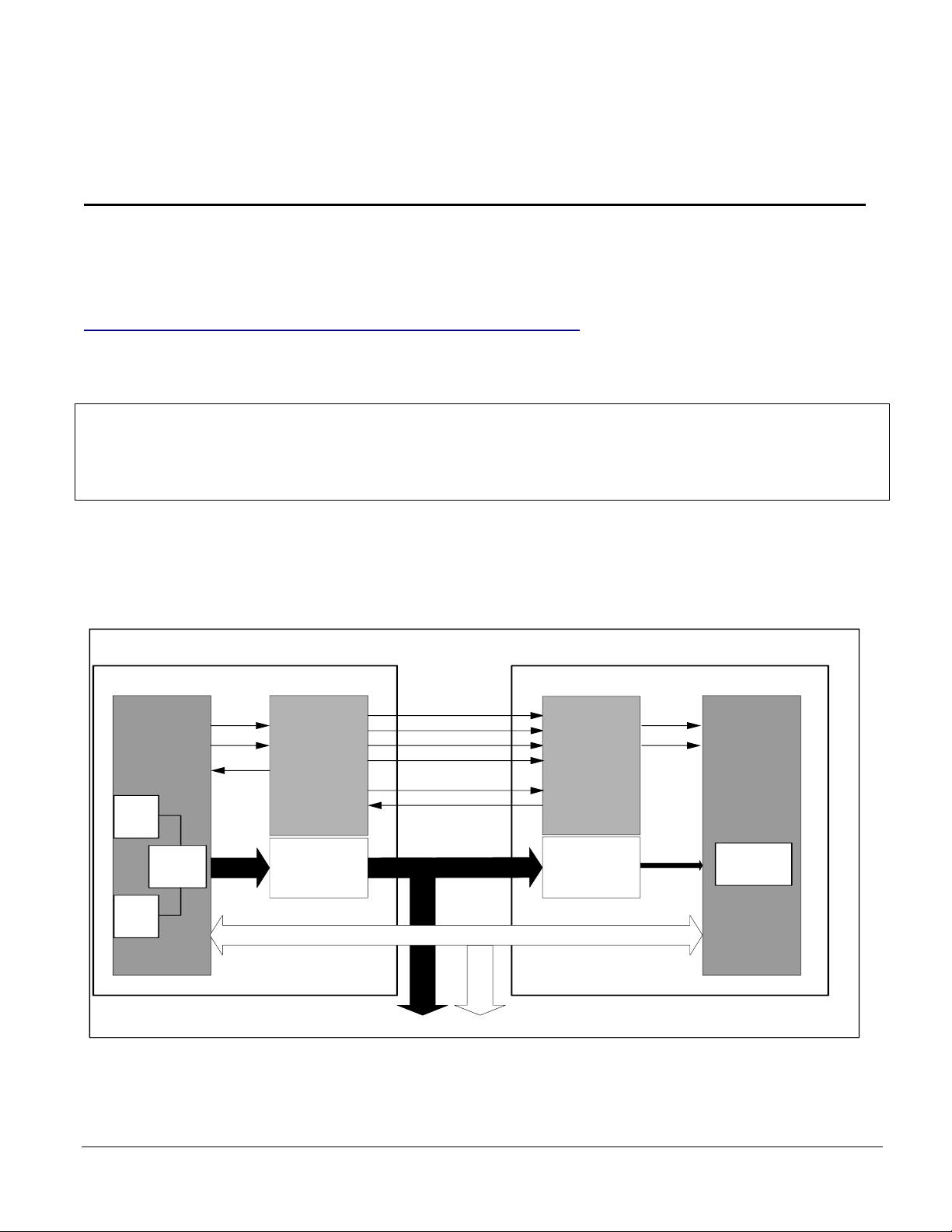
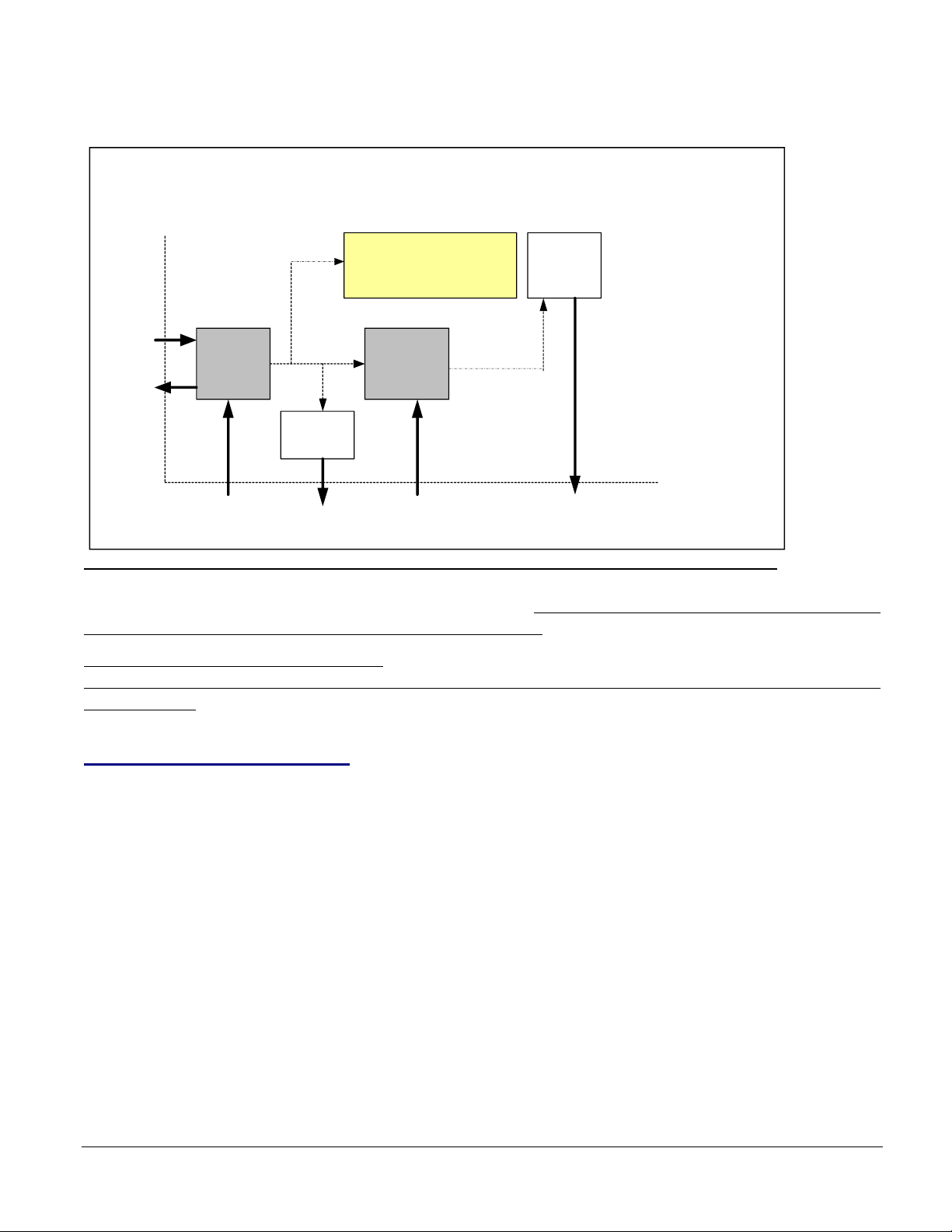
1 – ADSP-2116x Multiprocessing Signal Chain
Figure 1 illustrates the signal chain between two ADSP-21160s.
The 4 blocks for the signal flow are considered:
• Master (core, IOP, address buffer)
• Sync burst controller as encoder (master)
• Sync burst controller as decoder (slave)
• Memory (slave)
The controller works bi-directionally generating and decoding commands. CLKIN is the reference signal
and it is used for the synchronous operation. The Master’s internal strobes are converted to the sync burst
protocol. On the slave side, the commands are registered, decoded and transferred to the slave’s memory.
In the multiprocessor memory space (MMS), the slave’s ACK pin is used to control these transfers.
Moreover, the burst improves the DMA throughput for reads.
Figure 1: Signal chain: Interprocessor Transfer
AD SP-21160 M aster
int. R D
int. W R
int. A CK
core
~RDH
~RDL
d
n
e
~W RH
a
c
a
~W R L
m
f
r
m
e
t
o
n
I
C
BRST
ACK
~RDH
~RDL
~W RH
AD SP-21160 Slave
~W RL
BRST
ACK
t
s
c
i
r
g
u
o
B
L
int. RD
int. W R
IO P
Address
bu ffer
D63:0
A19:0
Address
Map/
Latch
A22:0
A31:0 D63:0
Address
Map/
Latch
A1:0
(Bu rst)
memory
D63:0
EE-165: The ADSP-2116x On-chip Sync Burst Controller Page 5 of 43
Page 6
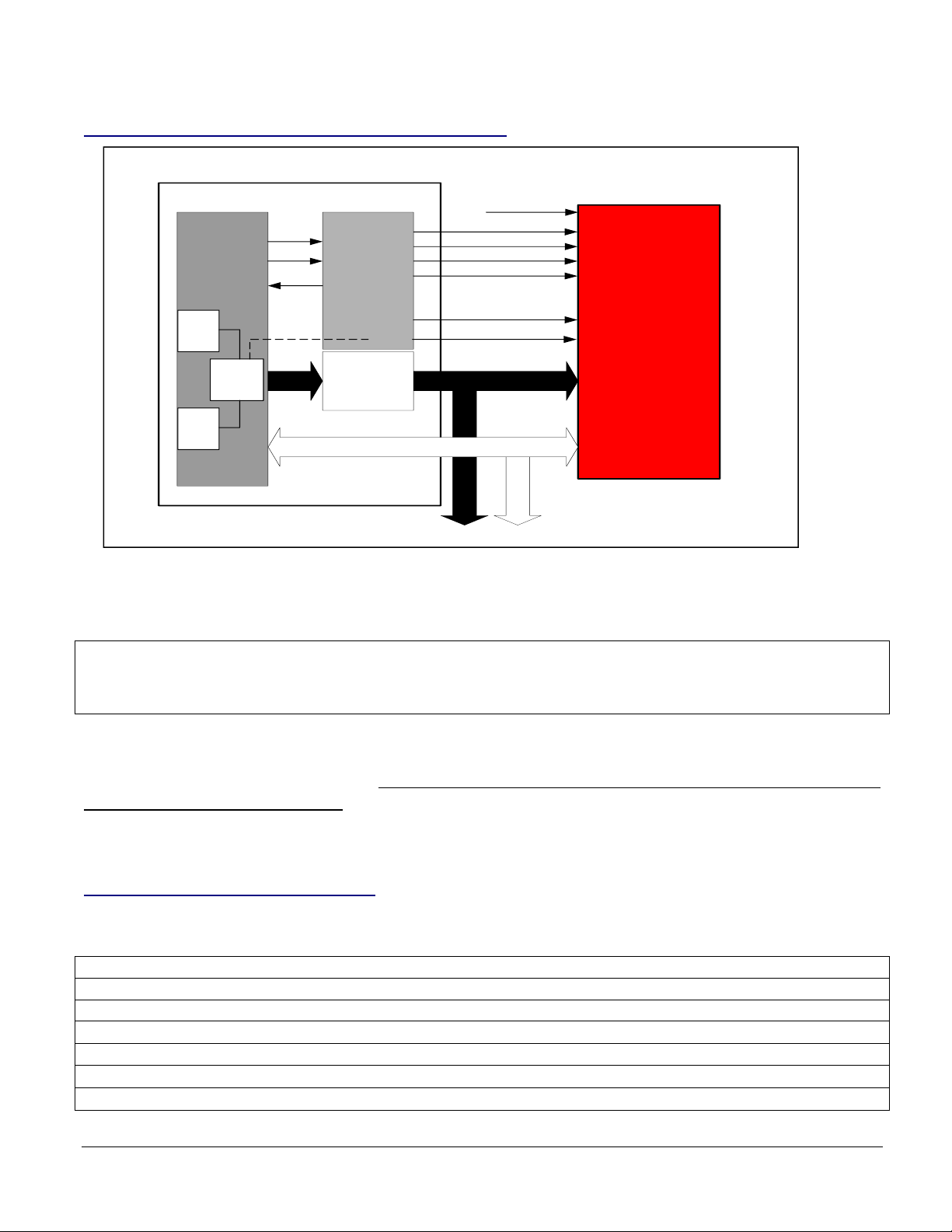
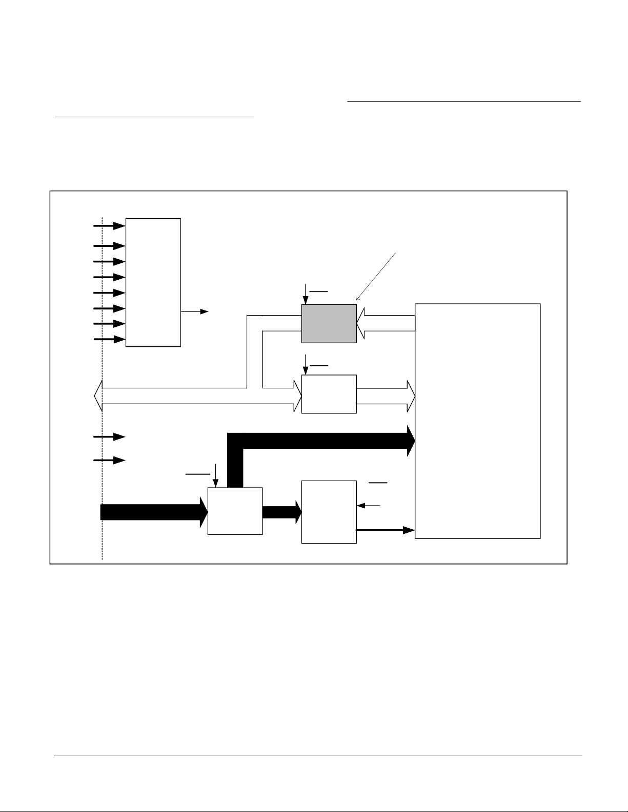
2 – ADSP-2116x SBSRAM Signal Chain
Figure 2: Signal chain: ADSP-21160 to SBSRAM
=
ADS P-21160 Master
int. RD
int. WR
int. A CK
core
A19:0
Address
buffer
IO P
D63:0
d
n
e
c
a
ma
f
r
m
e
t
o
n
I
C
~MS x
Address
Map/
Latch
~RDH
~RDL
~W RH
~W RL
BRST
A17:1
CLKIN
A31:0 D63:0
CLK
~OEL
~OEH
~GW H
~GW L
~ADSC1
~CE
A17:0
DQ63:0
SBSRAM
256k x 64
Figure 2 illustrates the signal chain between the ADSP-2116x, and an external SBSRAM.
The 3 parts for the signal flow to be considered are:
• Master (core, IOP, address buffer)
• Sync burst controller as encoder (master)
• SBSRAM
The signal chain is basically the same as for MMS. The main difference is that SBSRAM is a passive
device and never will be a bus master. The ADSP-2116x bus master writing to MMS or external memory
uses the same synchronous timing.
3 – External Port Interface
3.1 – Pin Description ADSP-21160
Pin State Description
CLKIN (I) clock input
~MSx (O/T) bank memory select line, chip enable
~RDL (I/O/T) initiates a read from an even address
~RDH (I/O/T) initiates a read from an odd address
~WRL (I/O/T) initiates a write to an even address
~WRH (I/O/T) initiates a read to an odd address
EE-165: The ADSP-2116x On-chip Sync Burst Controller Page 6 of 43
Page 7

BRST (I/O/T) starts the burst counter
ACK (I/O/S) acknowledge, slave control
D[31:0] (I/O/T) data for even address lines
D[63:32] (I/O/T) data for odd address lines
A[31:0] (I/O/T) address lines
I=input, O=output, T=Hi-Z, S=synchronous
3.2 – Pin Description ADSP-21161
Pin State Description
XTAL (O) output for crystal
CLKIN (I) clock input
~MSx (I/O/T) bank memory select line, chip enable
~RD (I/O/T) initiates a read
~WR (I/O/T) initiates a write
BRST (I/O/T) starts the burst counter
ACK (I/O/S) acknowledge, slave control
D[47:16] (I/O/T) data
A[23:0] (I/O/T) address lines
I=input, O=output, T=Hi-Z, S=synchronous
=
XTAL
On ADSP-21161, a crystal used in conjunction with the CLKIN pin can also generate the clock signal.
CLKIN
This pin is used to guarantee the SBSRAM’s synchronous operation. All addresses and commands are
latched on the positive edge of clock.
Bank Select (~MSx)
This pin is used to access the external device. It is used to sample the external address and command.
Provides address decoding and act as a chip selects for external memory mapped devices. For ADSP21160, the MSIZE bit in SYSCON defines the size for the 4 banks. For ADSP-21161, the bank sizes are
fixed, unbanked memory is not available.
ADSP-21160 Strobes (~RDx, ~WRx)
These pins are sampled to execute read or write operations. Since the ADSP-21160 is a full SIMD
machine, it uses two pairs of strobes for the external 2x32 bit data bus. The ~WRH and ~RDH are
decoded for odd addresses while ~RDL and ~WRL are decoded for even addresses.
ADSP-21161 Strobes (~RD, ~WR)
The ADSP-21161 uses the conventional ~WR and ~RD for the external 32 bit data. It’s internally a full
SIMD machine, but not externally.
Burst (BRST)
Burst feature is implemented to improve read performance. This line is asserted to start a bursting
operation. Burst operations are valid for DMA transfers only. If the burst feature is not needed, tie the pin
low. Partial data bus width transfers are not supported
EE-165: The ADSP-2116x On-chip Sync Burst Controller Page 7 of 43
.
Page 8
Note: ADSP-21160 supports burst for 64bit data only.
Note: ADSP-21161 supports burst for 32bit data only.
Acknowledge (ACK)
=
The ACK pin is used to extend external asynchronous and synchronous accesses
completion of an external access. In asynchronous mode, ACK is not sampled until the programmed
numbers of wait states have been counted. SBSRAM requires no slave control; ACK is tied high with an
internal pull-up resistance.
Following for synchronous mode:
2 cycles read: slave must assert ACK at least twice for each access (addresses/commands and data must be
acknowledged by the salve)
1 cycle write: ACK deasserted to extend the access by one cycle.
Used to extend the wait states by external devices.
Note: The ACK timing in MMS has changed between ADSP-2106x and ADSP-2116x family.
3.3 – Command Truth Tables
This section provides a table to get an overview of all commands provided by the Sync Burst controller.
These commands are handled automatically by the interface.
ADSP-21160
. It is used to hold off
Command Data Address ~MSx BRST ~RDH ~RDL ~WRH ~WRL
Read SISD 32-bit
Read SISD 32-bit
Read SIMD 64-bit All 0 0
Read Burst 64-bit All 0
Write SISD 32-bit
Write SISD 32-bit
Write SIMD 64-bit All 0 0 1 1
Write Burst 64-bit All 0
Deselect x x 1 x x x x x
ADSP-21161
Command Data Address ~MSx BRST ~RD ~WR
Read 32-bit All 0 0
Read Burst 32-bit All 0
Write 32-bit All 0 0 1
Write Burst 32-bit All 0
Even
Odd
Even
Odd
0 0 1
0 0
1 0 0
0 0 1 1 1
0 0 1 1
1
1 0
1
0
0 0
1 1
0
1
0
1 1 1
1
1
0
0
1 1
1 1
1 1
0
0 0
0 0
0
1
EE-165: The ADSP-2116x On-chip Sync Burst Controller Page 8 of 43
Page 9
=
Deselect x x 1 x x x
Setup and Hold Times
The synchronous operation uses the CLKIN as reference. Commands, addresses and data are latched at the
rising edge of CLKIN. The valid time margin around the rising edge is defined as setup time (time before
rising edge) and hold time (time after rising edge) to guarantee that both the controller encoder and
decoder are working reliably together. Signal’s- slew rates, propagation delays (PCB) and capacitive loads
(devices) influence these parameters and should be taken into consideration. The controller’s timing
characteristics are available in the ADSP-2116x datasheet.
3.4 – Clock Derivation
ADSP-21160
Figure 2a: External Port Clock Derivation ADSP-21160
External Port
Host
M u lt iproces s ing
SRAM, SBSRAM
PLL
core
clock
CLKIN
input
clock
Bus
master
CLKOUT
PLL
x2, x3, x4
CLK_CFG3:0
The clock source must be derived from an external oscillator for the ADSP-21160. The external port
interface (figure 2a) is internally connected with the CLKIN signal. The maximum speed for the external
port is 40 MHz for ADSP-21160M and 47,5 MHz for ADSP-21160N. The CORE:CLKIN ratio depends
only on the hardware pin settings CLK_CFG[3:0]. This ratio cannot be changed dynamically. The
CLKOUT pin is only driven during busmasterchip.
EE-165: The ADSP-2116x On-chip Sync Burst Controller Page 9 of 43
Page 10
ADSP-21161
=
Figure 2b: External Port Clock Derivation ADSP-21161
External Port
CLKIN
XTAL
Clock
Doubler
x1, x2
~CLKDBL
PLL
input
clock
Bus
master
CLKOUT
Host
M u lt iproces s ing
SRAM, SBSRAM
PLL
x2, x3, x4
CLK_CFG1:0
core
clock
SDRAM
x1, x1/2
SDCLK1:0
The clock source can be derived from an external oscillator or a crystal for the ADSP-21161. The external
port interface (figure 2b) is internally connected with the output of the clock double unit. The maximum
speed for the external port is 50 MHz for ADSP-21161N. The CORE:CLKIN ratio depends only on the
hardware pin settings CLK_CFG[1:0] and the ~CLKDBL pin. This ratio cannot be changed dynamically.
The maximum crystal speed is 25 MHz. With ~CLKDBL tied low, the external port speed is also 50 MHz.
Using a crystal does not allow the access to an SBSRAM. The CLKOUT pin is only driven during
busmasterchip. Additional, the SDRAM interface’s speed is depending on the core clock speed only.
4 – SBSRAM Technology
When synchronous memories use a pipelined architecture (registers for in- and output signals) they
produce additional performance gains. In a pipelined device, the internal memory array needs only to
present its data to an internal register to be latched rather than pushing the data off the chip to the rest of
the system. Because the array only sees the internal delays, it presents data to the latch faster than it would
if it had to drive it off chip. Further, once the latch captures the array’s data, the array can start preparing
for the next memory cycle while the latch drives the rest of the system.
The SBSRAM is basically an advanced architecture from the classical asynchronous SRAM. (like the
SDRAM from the DRAM) The design is static and requires typically 6 transistors to store 1 bit of
information. The interface’s control lines are sampled synchronously on the positive edge of the system
clock. Therefore, timing is self-timed internally. The memory vendors offer standard- and zero bus
turnaround architectures.
EE-165: The ADSP-2116x On-chip Sync Burst Controller Page 10 of 43
Page 11

=
4.1 – SBSRAM Architectures
The architecture can be described in 3 parts (figure 3):
Note: The partial (byte) writes capability, sleep- and suspend modes are not discussed; since they are not
supported by the ADSP-2116x DSPs.
Command Unit
Most of the control pins are registered with the rising edge of clock. These pins are grouped to device
select pins (~CE1, CE2, ~CE3). Another group is responsible for the burst logic (~ADSC, ~ADSP,
~ADV). The ~GW pin, sampled during CLK, controls the read and write operations.
Note: The ~OE pin is fully asynchronous and just used to enable the read output buffers.
Burst Unit
The input address latch plays an important role to support the burst counter. Firstly, the address is latched.
The Deassertion of ~ADSP or ~ADSC on the burst logic freezes the buffer’s input address clock (BCLK)
and clears the burst counter (CLR). The next addresses (linear or interleaved) are now internally
incremented. At the end of burst, ~ADSP or ~ADSC are asserted. Then, the input address is latched again.
Note: The ~ADV pin must be low during burst; otherwise the 2 bit counter does not count.
Note: The Mode (LBO) pin selects between linear and interleaved burst counting.
Register Units
The input- and output registers latch data on the rising edge of clock. The flow-through does not use an
output register like the pipelined architecture.
Note: The registers for address and data make the burst efficient.
4.2 – Standard SBSRAM
Micron Technology originally offered the Standard SBSRAM in 1996 for L2 cache applications. The
synchronous operation, which simplifies the design by shorter setup- and hold times, incorporates a burst
feature (2 bit burst counter) allowing a higher throughput during read operations. To offer these devices
over a large frequency bandwidth, subgroups are available like Pipelined- and Flow-through types (figure
4).
Flow Through
This partial pipelined architecture enables the read buffers and the data just flow through the output. Here
is a good compromise between speed and throughput < 66 MHz. The flow through type gives a
performance of 2-1-1-1 for a burst read.
Pipelined
EE-165: The ADSP-2116x On-chip Sync Burst Controller Page 11 of 43
Page 12
=
This architecture registers and enables the read buffers and the data flow through the output. This is used
to improve the performance for high-speed applications. Above 66 MHz, the pipelined devices offer a
clear advantage in terms of performance. For instance, at 100 MHz the pipelined version results in 3-1-1-1
in comparison to a flow through of 3-2-2-2. The pipeline technique helps to fetch, deliver, and capture
subsequent data.
Figure 3: Simplified SBSRAM Arc hit ec t ure 512k x 32 bit
CLK
~CE1
CE2
~CE3
~ADV
~ADSP
~ADSC
~GW
Command
and
Burst
Logic
GW,
CLR,
CLK,
BCLK
(byte write logic ignored)
flow-through version
does not use
registered output buffer
CLK, OE
Output
Buffer
DQ31:0
~OE
Mode
A18:2
A1:0
BCLK
Input
Address
Buffer
A16:0
CLK, GW
Input
Buffer
Address
Latch
Burst
Counter
A18:0
CLK,
Mode,
CLR
A1:0
Memory Core
(512k x 32bit)
EE-165: The ADSP-2116x On-chip Sync Burst Controller Page 12 of 43
Page 13
CLK
~OE
~GW
ADDR
Data
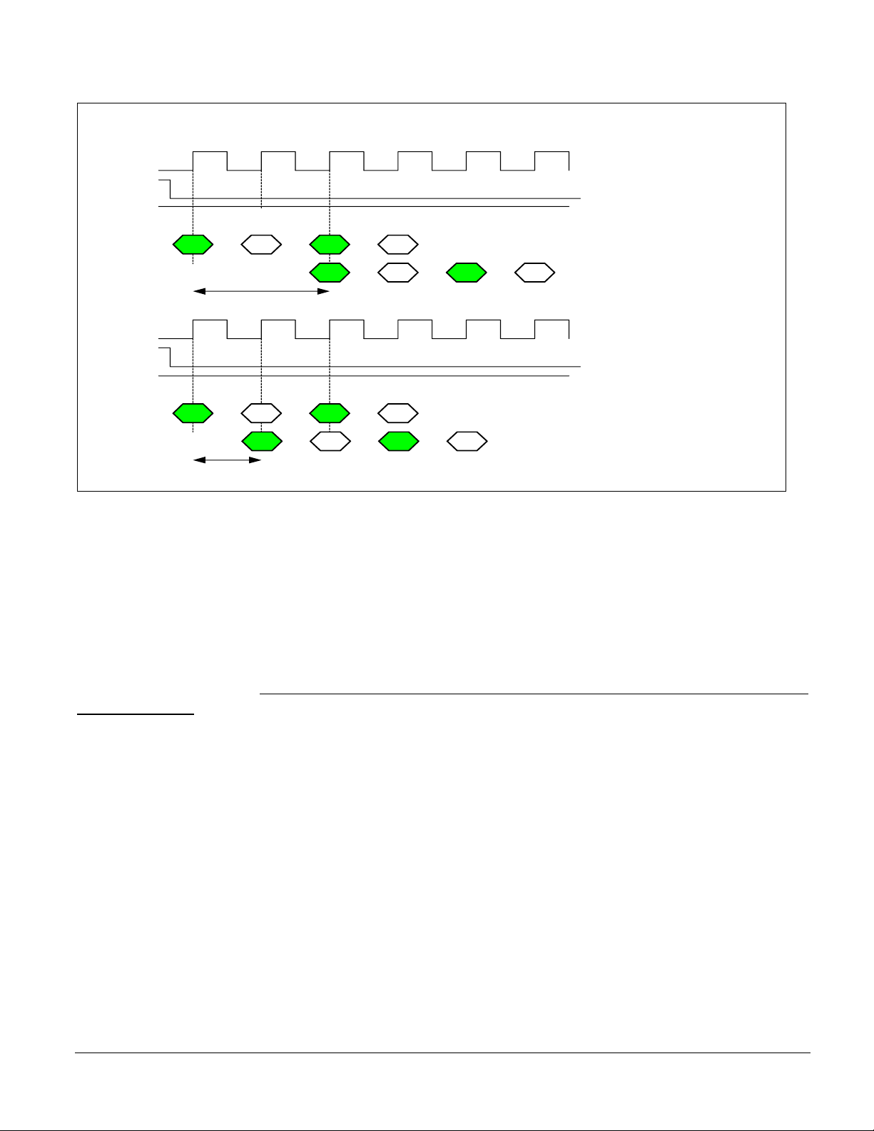
Figure 4: Standard SBSRAM s, pipelined vs. flow through for random reads
e
p
i
P
Read operation requires 3
cycles between latching the
A1
A2A4 A5
Q1
Q2Q4 Q5
address and driving data
BL=4, performance 3-1-1-1
=
d
e
n
i
l
CLK
~OE
~GW
ADDR
Data
A1
2 cycles
3 cycles
Q1
A2A4 A5
Q2Q4 Q5
t
Read operation requires 2
cycles between latching the
address and driving data
BL=4, performance 2-1-1-1
F
h
w
o
l
o
r
u
g
h
Note: For lower frequency, the flow through is best choice, for higher frequency, the pipelined version is
dominant.
4.3 – Zero Bus Turnaround SBSRAM
The ZBT- or No Bus Latency (NoBL) SBSRAM was originally offered by Integrated Device Technology
in 1999. The basic difference between the standard- and ZBT types resides in the access mode. For
network applications, typically where back-to-back read to write are used. The ZBT was created in
response to applications, which require frequent bus turnarounds but could not afford the stall cycles
needed by standard types. The trick is that all read and write accesses have the same fixed offset between
address and data. So, no dead cycles between write ands reads (figure 5).
Flow Through
Just like standard SBSRAM (section 4.2)
Pipelined
Just like standard SBSRAM (section 4.2)
EE-165: The ADSP-2116x On-chip Sync Burst Controller Page 13 of 43
Page 14

=
Figure 5: ZBT/NoBL SBSR AM s, pipelined vs. flow through for random read to writes
CLK
~OE
~GW
ADDR
Data
CLK
~OE
~GW
ADDR
Data
A1
3 cycles
A1
D1
2 cycles
A2A4 A5
D1
A2A4 A5
D2Q4 Q5
D2Q4 Q5
Note: The ZBT SBSRAM is designed for frequent read to write transitions.
d
e
n
i
l
e
p
i
P
BL=4, performance 3-1-1-1
u
o
r
h
t
w
o
l
F
BL=4, performance 2-1-1-1
g
h
4.4 – Pin Description SBSRAM
Switched Pins Type Description Note
CLK (I) system clock connect to CLKIN
SA[X:2] (I) synchronous addresses connect to A[X:3]
SA[1:0] (I) synchronous burst addresses connect to A[2:1]
DQ[X:0] (I/O) data connect to D[63:0]
~GW (I) global write connect to ~WRx
~CE (I) chip enable connect to ~MSx
~ADSC (I) address status controller connect to BRST
~OE (I) asynchronous output enable connect to ~RDx
Fixed Pins
~BWE (I) byte write fixed to VDD
CE2 (I) chip enable 2 fixed to VDD
~ADSP (I) address status processor fixed to VDD
~BWx (I) byte write selects fixed to VDD
~CE2 (I) chip enable 2 fixed to GND
~ADV (I) address advance fixed to GND
Mode/LBO (I) selects burst counting fixed to GND
ZZ (I) snooze/sleep mode fixed to GND
Note: The ADSP-2116x DSPs only use the SBSRAM features partially.
EE-165: The ADSP-2116x On-chip Sync Burst Controller Page 14 of 43
Page 15

=
4.5 – Memory Organizations
The personal computer (PC) market offers parity and non-parity sizes. Data integrity checking that adds a
single bit to each byte of data. The parity bit is used to detect errors in the other 8 bits. The 2116x DSPs
don’t support the parity bits. Therefore, the DQP pins should simply be tied to GND with a weak pull
down resistor.
Size Type Parity Bits
1 Mbits/ 128 kbytes 32k x 32
32k x 36
64k x 18
2 Mbits/ 256 kbytes 64k x 32
64k x 36
128k x 18
4 Mbits/ 512 kbytes 128k x 32
128k x 36
256k x 18
8 Mbits/ 1 Mbytes 256k x 32
256k x 36
512k x 18
16 Mbits/ 2 Mbytes 512k x 32
512k x 36
1M x 18
-4
2
-4
2
-4
2
-4
2
-4
2
4.6 - SRAM vs. SBSRAM
The burst mode is a very high-speed access mode bringing an internal address generator into play. Once an
address for the first access is set, sequential addresses are automatically build by the internal column
address counter. The next table summarizes the differences:
SRAM SBSRAM
No system clock Runs off system clock
edge control pulsed level control, internally self timed
no address pipeline address pipeline
no burst capability burst length 4
non-programmable Read latency flow through or pipeline for different speeds
5 – Sync Burst Controller Characteristics
This chapter describes the controller’s characteristics:
5.1 – Multiprocessing Memory Space
In MMS, the controller’s wait state settings are fixed to:
• 2 cycles reads minimum
• 1 cycle writes maximum
EE-165: The ADSP-2116x On-chip Sync Burst Controller Page 15 of 43
Page 16

=
5.2 – Core Transfers
Core transfers work without address pipelining. After latching the current read address, the next address
can only be latched after the current data is driven off chip.
Note: SHARC architecture does not support address pipelining.
5.3 – DMA Transfers
The controller simply assumes that the next address is sequential in burst mode. It latches all following
data cycle by cycle in order to improve the throughput for sequential DMA reads. The controller drives the
first address, then the slave’s burst counter will modify the next 3 sequential addresses. The burst count
mode must be set to sequential by the SBSRAM’s MODE/LBO pin.
Burst Enable
The DMA controller starts the DMA burst operation (figure 6) by assertion of the BRST pin under
following conditions only:
MAXBL(1-0) bit in DMACx must be set
ECx ≥ 4 (number of 32-bit words)
EMx = 0 or 1 (forced to SIMD)
CLK
~RDL
~RD H
ADDR
Data(31:0)
Data(63:32)
CLK
~RDL
~RDH
ADDR
Data(31:0)
Data(63:32)
BRST
Figure 6: SBSRAM: Core vs. DMA Transfers for 4x32-bit reads
A0/1
A0/1
D0
D1
A2/3
D0
D1 D3
A2/3
D2
D2
D3
The dotted address is
incremented by the slave's
burst counter
C
D
o
M
r
e
A
Note: ~HBR assertion does not receive ~HBG until the burst finishes.
Note: The burst DMA read throughput is 2-1-1-1 compared to 2-2-2-2 for core operation.
EE-165: The ADSP-2116x On-chip Sync Burst Controller Page 16 of 43
Page 17

=
Burst Length
The table will show, how the controller defines the burst length, depending on the word count.
DMA ECx counter 3 4 5 6 7 8 9 10 11 12
Pin BRST cycles 0 1 1 2 2 3 3 3 3 3
Burst length 0 2 2 3 3 4 4 4 4 4
Note: The controller uses unaligned access for odd values of ECx in burst mode.
5.4 – Deselect Cycle
Under the following situations, the controller issues a deselect (idle) cycle:
• read to write transition
• bank- or MMS transitions (slave’s ACK tristated)
• core access (DAG, computation unit, interrupt, cache)
• ~HBR (host interface)
• ~BRx (multiprocessing)
Note: For the ADSP-2116x, the use of ZBT SBSRAMs is not so efficient, the controller issues
automatically a bus idle cycle for each read to write transition.
5.5 – ADSP-21160 External Port Address Mapping
The DSP is designed as a full SIMD machine, internally and externally supported
. Because of external
SIMD capability, external code execution and boot memory, different address mapping scheme become
necessary. Following memory address decoding scheme is used:
ADDR[0:7] IOP space
ADDR[8:16] Internal memory
ADDR[17:19] S-field, internal memory
ADDR[20:22] M-field, MMS
ADDR[21:31] E-field, external memory
32-bit Data Transfers
The DSP uses the memory select pins (~MSx), and two pairs of strobes (RDx, WRx). Each strobe can
individually select a 32-bit word, depending on even (low strobes) or odd address (high strobes) when
declared as 32-bit section in the Linker Description File (LDF). For data accesses, the A[0] pin becomes
redundant for SBSRAM and MMS transfers. The LSB state is already decoded in the high and low lane of
the strobe. Therefore, the SHARC’s address A[0] is not connected to the SBSRAM
. In order to support the
SIMD feature externally, each strobe selects a word in the same cycle. The DSP only supports normal
word addressing in external memory (no long and short word).
40-bit Data Transfers
Both strobes select a 40-bit word in one CLKIN cycle when declared as 40-bit section in the LDF. The
lower data pins [23:0] are ignored during these transfers. The DSP uses the same address mapping as for
32-bit transfers. To move data or instructions to or from external memory, programs should use the PX
register as an intermediate 64-bit holding register.
EE-165: The ADSP-2116x On-chip Sync Burst Controller Page 17 of 43
Page 18

=
Note: When viewing data memory, the format representation used should be hexadecimal for 40-bit data.
The bus alignment will then help to understand both data portions of the low- and high strobes.
48-bit Opcode Fetches
The interface supports code instruction fetch from x48, x64 wide memories only. Both strobes select a 48bit word in two CLKIN cycles when declared as 48-bit PM section in the LDF. The program sequencer
uses the full address bus including address A[0]. The SHARC’s address A[0] is connected to the
SBSRAM One address during code fetch requires 2 addresses for data access. The address mapping for
code fetching uses half the address size compared to SIMD address mapping in SBSRAM. Therefore, the
controller changes the address mapping. During the fetch, the lower data pins [15:0] are ignored.
Note: The sequencer does not use the burst protocol.
8-bit PROM/FLASH Transfers
During boot mode, the DSP uses the upper strobes only (~RDH, ~WRH) to select the Boot Memory with
~BMS. It uses the full address bus including address A[0]. The SHARC’s address A[0] is connected to the
boot memory. Again, it uses here a different address mapping scheme.
Next table compares the different access modes:
CLKIN cycles
1
2
3
4
Note: For debug, use the two columns memory window for data access and the tree columns memory for
code fetching in SBSRAM.
64-bit Memory
The connection of 2x32 bit gives the highest throughput.
Note: Only 64 bit data transfers allow burst access.
8/32-bit Memory
All memory sizes smaller than 64-bit can be connected to the external port interface. But with restriction:
choosing even or odd address limits the address modifier to a minimum of 2.
5.6 – ADSP-21161 External Port Address Mapping
~MSx(32,40,64-bit) ~CIF(48-bit) ~BMS(32-bit)
0x800000 0x800001 0x800000 0x000000
0x800002 0x800003 0x800001 0x000001
0x800004 0x800005 0x800002 0x000002
0x800006 0x800007 0x800003 0x000003
The DSP is designed as partial SIMD machine, it is internally supported.
Following memory address decoding scheme is used:
ADDR[0:8] IOP space
ADDR[9:16] Internal memory
EE-165: The ADSP-2116x On-chip Sync Burst Controller Page 18 of 43
Page 19

=
ADDR[17:19] S-field, internal memory
ADDR[20] M-field, MMS
ADDR[21:23] E-field, external memory
ADDR[24:25] V-field, zeros
ADDR[26:27] V-field, ~MSx
32-bit Data Transfers
The DSP uses the memory select pins (~MSx), and strobes (RD, WR) to access external memory. The Efield is limited up to address 23 and the addresses 24-25 are zero. The V-field (virtual) represents the
memory select lines and extends the address space. Therefore, external memory space for SBSRAM is not
continuous. The DSP only supports normal word addressing in external memory (no long and short word).
40-bit Data Transfers
Transferring extended precision data is supported using the PX register. It transfers the 40-bit as a 48-bit
data by zero filling the 8 LSBs. Two accesses should be done to fill the PX register over the 32-bit bus.
48-bit Opcode Fetches
The interface supports code instruction fetch from x8, x16, x 32, x48 wide memories when declared as 48bit PM section in the LDF. The IPACK bits in SYSCON register defines the packing. Writing to the
SYSCON to enable the packing mode, delay the instruction fetch by 2 instructions. Code execution is only
allowed for bank 0
Note: The sequencer does not use the burst protocol.
8-bit PROM/FLASH Transfers
During boot mode, the DSP uses (~RD, ~WR) to select the Boot Memory with ~BMS.
6 – Programming the Sync Burst Controller
The Controller is programmed through the wait register (WAIT) to provide the SBSRAM’s synchronous
timing. The specific modes like sleep, burst- length and count are determined by hardware through the
dedicated SBSRAM pins.
Note: The SBSRAM memory device is not programmed by software like the SDRAM memory device.
6.1 – Access Mode
For proper synchronous operation, make sure that the dedicated WAIT register setting is configured to:
• EBxAM=01-02 1 – 2 cycles writes (read wait states depends on EBxWS only)
Note: EBxAM = 00 is for asynchronous memory, 11 is reserved.
EE-165: The ADSP-2116x On-chip Sync Burst Controller Page 19 of 43
Page 20

=
6.2 – Wait State Mode
For proper read operation, make sure that the dedicated WAIT register setting is configured to:
• EBxWS=01-07 2 – 8 cycles reads (write wait states depends on EBxAM only)
EBxWS=0, zero Wait State for Reads is not supported.
Note: writes are fixed to 1 – 2 cycles (EBxAM), if longer access time is required, use ACK to extend the
wait mode.
6.3 – Burst Mode
For write burst transfers, the EBxAM value must be set to 2
performance, as opposed to using 1 cycle write with no burst.
Note: The MAXBL bit (DMACx) enables the DMA burst transfers operations.
6.4 – Burst Setting Overview
SBSRAM 1 cycle write 2 cycles write 2 cycles read
Master DMA No
Core No No No
Note: The Write burst capability requires 2 cycle’s writes.
MMS 1 cycle write 2 cycles read
Master DMA No
Slave DMA No
Core No No
Note: Only Read DMA should use burst capability to improve the performance.
6.5 – Example
Data sheet of a vendors 256K x 16 bit:
Yes Yes
Yes
Yes
. However, this will cause a degradation of
• 4Mbit
• CLKIN= 40 MHz
• Read Flow through Architecture => read outputs are not registered
• Speed grade = 9
• Read Performance @ 40 MHz: =>2 cycle read (2-1-1-1)
• Write Performance @ 40 MHz: =>1 cycle write
• Mapped to ~MS0 of SHARC
SBSRAM: ustat1=0x01CE7385; /* synchr. Access bank 0 */
dm(WAIT)=ustat1; /* 1 cycle write, 2 cycles read */
EE-165: The ADSP-2116x On-chip Sync Burst Controller Page 20 of 43
Page 21

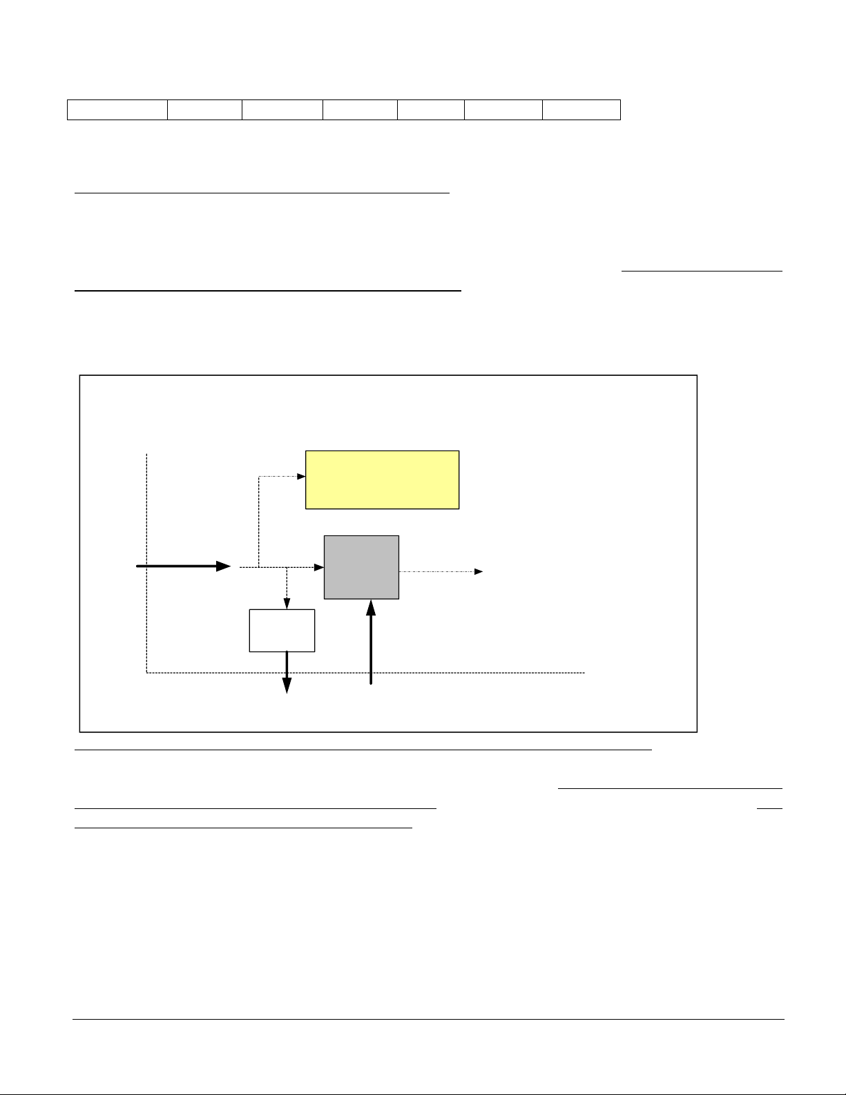
Figure 7: Simplified State Diagram: ADSP-2116x SBSRAM Controller
=
Core
Read
MSx
MMS
Core
IOP MMS
Host
DMA
Read
MSx
MMS
Wait
States
Wait
States
Idle
Wait
States
Wait
States
Core
Write
MSx
MMS
Power
up
DMA
Write
MSx
MMS
WS to MMS are f ixed to :
1 cycle write maximum
2 cycles read minimum
WS to SBSRAM are
configurable to :
1 cycle write minimum
2 cycles read minimum
DMA wr i te burst supported
for 2 cycles wr ites only
Burst counter =4
Burst counter =4
Note: The minimum spec must be guaranteed. Higher settings cause a degradation of performance only.
7 – Sync Burst Interface after Reset
When the ADSP-2116x ~Reset pin is deasserted, the external port interface is in following state:
• EBxAM=00 asynchronous access mode for external memories
• EBxWS=07 7 wait states, required to access EPROM/Flash asynchronously during boot mode
Note: The MMS is fixed to synchronous timing.
8 – Single Word Transfers
The host interface allows an external controller (figure 8) to get directly control (highest priority with
~HBR) to transfer data to the SHARC or its external memory. When the SHARC responds with ~HBG to
EE-165: The ADSP-2116x On-chip Sync Burst Controller Page 21 of 43
Page 22

=
a host request ~HBR, it will start working in slave mode after a bus- and host transition cycle (BTC,
HTC).
8.1 – Host to DSP
The synchronous mode (~HBR=low, ~CS=high) allows accessing the MMS
another SHARC. To get it working, the SHARC’s ID number must be set to one
. The host acts just like
. The host writes
synchronously to the offset of 0x100000. DSP internally, the MMS is copied to the internal memory.
ADSP-21160 Description
ID set to one
~CS deasserted
~HBR asserted from host
~HBG grant from DSP
~RDx read strobes pair
~WRx write strobes pair
BRST initiates burst transfers
ACK acknowledge slave control
A[22:0] MMS address lines
DQ[63:0] data
Note: The SHARC’s ID=1 causes the assertion of ~BR1 during external accesses.
Note: ~CS low during ~HBR initiates an asynchronous access.
8.2 – Host to SBSRAM
Synchronous host allows transferring data directly to the SBSRAM, here the DSP acts only as bus arbiter.
After ~HBG is returned, the host selects the SBSRAM memory, and drives the signals directly to the
device. These transfers occur using the protocol of the SBSRAM peripheral. This mode acts like external
handshake DMA, but for single word transfers only. The synchronous host access is only valid for the
ADSP-21160.
Note: Synchronous host mode is not supported by the ADSP-21161.
9 – DMA Transfers
This chapter describes the different ways of transferring blocks of data between SBSRAM, host and
SHARC.
9.1 – DSP to SBSRAM
Master Mode
EE-165: The ADSP-2116x On-chip Sync Burst Controller Page 22 of 43
Page 23

=
In this configuration, the DMA parameter registers can be configured by the DSP’s own core, by another
SHARC in a multiprocessing system or by a host. In this mode, the DMA controller drives the bus and
initiates the transfers.
Parameter IIx IMx ICx EIx EMx ECx
Master Mode yes yes yes yes yes yes
Paced Master Mode
In this mode, the DMA controller cannot initiate the transfer, even though it is the bus master. An external
device controls the data transfer by toggling ~DMARx. It interprets the falling edge to begin a DMA
transfer and the rising edge to complete the DMA transfer. So, the pulse period of ~DMAR defines the
speed of the DMA operation. The data is transferred between the on-chip memory and SBSRAM (figure
6). Each time ~DMARx toggles (once per word transfer), the ECx counter is decremented. Accesses can
be extended by the ACK input, by programmed wait states and by holding ~DMARx low.
Note: The core to CLKIN ratio settings (CLK_CFG[x]) influence the speed of this transfer mode.
Parameter IIx IMx ICx EIx EMx ECx
Paced Master Mode yes yes yes yes yes yes
Note: The paced master mode is externally controlled with ~DMARx.
9.2 – Host to DSP
Handshake Mode
The host requests the bus with ~DMARx and the SHARC grants the bus with ~DMAGx to transfer a
single word. Each time ~DMARx is toggled the ECx counter is decremented. Address- and chip select
pins are not required.
Note: This kind of transfer is very effective, because the bus mastership is transferred for 1 cycle in
comparison to the host access (~HBR, ~HBG), where the bus is retained for several cycles.
Parameter IIx IMx ICx EIx EMx ECx
Handshake yes yes yes no no yes
Note: ~HBR must be deasserted for handshake mode.
Slave Mode
This is the classical mode for booting a SHARC via a host. The host requests with ~HBR and the SHARC
grants with ~HBG. For read, it waits until data is available in the buffers. For writes, it fills up the FIFO
until it is emptied.
Parameter IIx IMx ICx EIx EMx ECx
Slave Mode yes yes yes no no no
Note: ~HBR (host) or ~BRx (MMS) must be asserted to bring the device in slave mode.
EE-165: The ADSP-2116x On-chip Sync Burst Controller Page 23 of 43
Page 24

=
9.3 – Host to SBSRAM
External Handshake Mode
Here, the DMA controller does not initiate the transfer. A host requests (~DMARx) the bus to the SHARC
to access the SBSRAM directly. The SHARC’s grant pin (~DMAGx) initiates the data transfer from the
host to the SBSRAM.
Parameter IIx IMx ICx EIx EMx ECx
External Handshake Mode no no no yes yes yes
Note: ~HBR must be deasserted for external handshake mode.
Note: For external handshake, the SHARC’s EPBx buffers are untouched.
10 –ADSP-2106x vs. ADSP-2116x MMS Timing
10.1 – Wait States
ADSP-2106x: Wait states can be changed by setting the MMSWS bit (WAIT). Setting MMSWS to 1 will
add 1 wait state for reads and writes.
ADSP-2116x: This option is no longer available. The wait states are fixed for reads and writes.
Note: For ADSP-2106x, this option should be used whenever the external bus is heavily loaded.
10.2 – Reads
ADSP-2106x: address pipelining is not supported. Every time it latches an address, it automatically
deasserts the slave control ACK pin during first access cycle to block the next data. In the second cycle, it
drives the data off-chip at the rising edge (edge triggered input) of read strobe and asserts ACK.
Note: The RD and ACK pins toggle for each ADSP-2106x access in the “quasi synchronous” timing.
ADSP-2116x: Distinguish between core and DMA. For both, address pipelining is not supported. The 2
cycles read latches the address in the first cycle and drives the data when strobe is low during the rising
edge (level triggered input) of CLKIN. For DMA, the on-chip controller simply assumes the next address
to be sequential.
10.3 – Writes
ADSP-2106x: The data is valid on the rising edge (edge triggered input) of the write strobe.
Note: The WR pin toggles for each ADSP-2106x access in the “quasi synchronous” timing.
ADSP-2116x: The data is sampled when the write strobe is low during the rising edge (level triggered
input) of CLKIN.
Note: For ADSP-2106x and ADSP-2116x, completion of reads and writes depends only on the ACK
signal.
EE-165: The ADSP-2116x On-chip Sync Burst Controller Page 24 of 43
Page 25

11 – ADSP-21160 Code Execution from SBSRAM
Figure 9: Signal flow for data and code execution from SBSRA M
=
Cache
32x 48
bit
ADSP -21160
PMA
Controller
~CIF
sequencer
needs A0
~RDL
~RDH
SBSRAM
2x32 bit
Sequencer
PMD 47:0
23:0
Core Clock
A18:0
A23:1
Latch
no
packing
code
MUX
data
A0
redundant
Figure 9 demonstrates the signal flow for code execution from SBSRAM. The Program sequencer of the
ADSP-21160 issues a maximum of 24-bit PM addresses to the controller’s input. The controller’s pair of
read strobes point to an aligned 64-bit location in the SBSRAM. The 48-bit code is latched by the DSP to
get registered by the instruction pipeline. The DSP only asserts ~CIF during instruction fetches from
external memory. Therefore, this pin is helpful to switch between data accesses and 48-bit opcode fetching
from external memory. A[0] becomes redundant for data accesses, but not for opcode fetching
sequencer asserts ~CIF, ~RDL and ~RDH low in order to fetch the 48-bit portion of the SBSRAM with
the full address bus A[x:0]. For data access, the A[x:1] lines access the SBSRAM instead.
4x16 bit
A18:0
A23:1
DQ63:16
CLKIN
. The
The linker’s memory command in the VisualDSP++ linker description file (.LDF) is used to activate the
mode for code execution when the SBSRAM’s section is declared with PM width of 48bit:
Memory
{
seg_rth { TYPE(PM RAM) START(0x00040000) END(0x000400FF) WIDTH(48) }
.
.
bk0_pmco { TYPE(PM RAM) START(0x00800000) END(0x008FFFFF) WIDTH(48) }
}
Note: The sequencer’s 24-bit address allows program execution to the low 12 Mwords of memory map.
EE-165: The ADSP-2116x On-chip Sync Burst Controller Page 25 of 43
Page 26

=
The controller fetches (figure 10) each location with a 2 cycles read. The minimum ratio between Coreand CLKIN is 2:1. Therefore the ratio between the core and code execution is 4:1. Adding pipeline effects,
it takes 6 CLKIN cycles to execute the first instruction.
Figure 10: Code Execution, CLKIN:Core Ratio 1:2
Core
CLKIN
~MS0
~RDL
~RDH
A(23:0)
D(31:16)
D(63:32)
A0 A1 A2 A3
Q0 Q2
Instr.
Fetch
Instruction Pipeline 6 cycles
Q1 Q3
Q1 Q3Q0 Q2
Instr.
Decode
Instr.
Execute
Note: The maximum performance is 25 % compared to executing the same code in internal memory.
12 – Memory Access Types
12.1 – Internal Memory of ADSP-2116x
On ADSP-21160 and ADSP-21161, various access modes for transfers between the on-chip memory and
core are available. The following cases demonstrate some different access modes.
Normal Word SIMD, explicit even address
bit set mode1 PEYEN; // SIMD mode
b0 = 0x50000; // 32-bit block 1 even address
l0 = 0;
m0 = 2;
dm(i0,m0) = r0 ;
// core executes: dm(0x50000) = r0 , dm(0x50001) = s0;
Normal Word SIMD, explicit odd address
bit set mode1 PEYEN; // SIMD mode
b0 = 0x50001; // 32-bit block 1 odd address
l0 = 0;
m0 = 2;
dm(i0,m0) = r0 ;
// core executes: dm(0x50001) = r0 , dm(0x50002) = s0;
Long Word, explicit even address
EE-165: The ADSP-2116x On-chip Sync Burst Controller Page 26 of 43
Page 27

=
bit set mode1 PEYEN; // SIMD mode
b0 = 0x28000; // 64-bit block 1 even address
l0 = 0;
m0 = 2;
dm(i0,m0) = r0 ; // SIMD overridden
// core executes: dm(0x28000) = r0 , dm(0x28000) = r1;
Long Word , explicit odd address
bit set mode1 PEYEN; // SIMD mode
b0 = 0x28001; // 64-bit block 1 odd address
l0 = 0;
m0 = 2;
dm(i0,m0) = r0 ; // SIMD overridden
// core executes: dm(0x28001) = r0 , dm(0x28001) = r1;
Note: For long word accesses, the explicit value moves to LSB and implicit value to MSB of long word
address.
Forced Long Word, explicit even address
bit set mode1 PEYEN; // SIMD mode
bit set mode2 U64MAE; // unaligned access detection
b0 = 0x50000; // 32-bit block 1 even address
l0 = 0;
m0 = 2;
dm(i0,m0)(lw) = r0 ; // SIMD overridden
// core executes: dm(0x50000) = r0 , dm(0x50001) = r1;
// IRPTL bit IICD cleared
Forced Long Word , explicit odd address
bit set mode1 PEYEN; // SIMD mode
bit set mode2 U64MAE; // unaligned access detection
b0 = 0x50001; // 32-bit block 1 odd address
l0 = 0;
m0 = 2;
dm(i0,m0)(lw) = r0 ; // SIMD overridden
// core executes: dm(0x50000) = r0 , dm(0x50001) = r1;
// IRPTL bit IICD set
Note: The register file source or destination of a forced long word access (LW) is a set of two neighboring
registers in a processing element.
12.2 – External Memory of ADSP-21160
Normal Word SIMD, explicit even address
bit set mode1 PEYEN; // SIMD mode
b0 = 0x800000; // 32-bit bank 0 even address
l0 = 0;
m0 = 2;
dm(i0,m0) = r0 ;
// core executes: dm(0x800000) = r0 , dm(0x800001) = s0;
Normal Word SIMD, explicit odd address
bit set mode1 PEYEN; // SIMD mode
b0 = 0x800001; // 32-bit bank 0 odd address
l0 = 0;
m0 = 2;
dm(i0,m0) = r0 ;
// core executes: dm(0x800000) = r0 , dm(0x800001) = s0;
EE-165: The ADSP-2116x On-chip Sync Burst Controller Page 27 of 43
Page 28

Note: The external memory supports aligned SIMD accesses only.
Forced Long Word, explicit even address
bit set mode1 PEYEN; // SIMD mode
bit set mode2 U64MAE; // unaligned access detection
b0 = 0x800000; // 32-bit bank 0 even address
l0 = 0;
m0 = 2;
dm(i0,m0)(lw) = r0 ; // SIMD overridden
// core executes: dm(0x800000) = r0 , dm(0x800001) = r1;
// IRPTL bit IICD cleared
Forced Long Word, explicit odd address
bit set mode1 PEYEN; // SIMD mode
bit set mode2 U64MAE; // unaligned access detection
b0 = 0x800001; // 32-bit bank 0 odd address
l0 = 0;
m0 = 2;
dm(i0,m0)(lw) = r0 ; // SIMD overridden
// core executes: dm(0x800000) = r0 , dm(0x800001) = r1;
// IRPTL bit IICD set
=
12.3 – External Memory of ADSP-21161
For the 32-bit external memory, the SIMD, long and forced long word accesses are not supported.
12.4 – Memory Access Types Summary
ADSP-21160/21161 internal memory:
• SIMD mode allows aligned and unaligned access.
• U64MAE bit (MODE2) helps to detect an unaligned long word access to generate an interrupt
(IICDI).
ADSP-21160 external memory:
• SIMD forces all access types to be aligned.
• U64MAE bit (MODE2) helps to detect an unaligned long word access to generate an interrupt
(IICDI).
• External memory can only be accessed in normal word.
ADSP-21161 external memory:
• External memory does not support SIMD and long word.
Note: If you do not use SIMD, turn the PEY processing unit off. This guarantees an optimized usage of
memory in SISD mode.
EE-165: The ADSP-2116x On-chip Sync Burst Controller Page 28 of 43
Page 29

=
13 – Optimizing the Performance
13.1 – Throughput for Reads
Next table will illustrate the different synchronous read throughputs in CLKIN cycles/word, caused by the
SHARC’s read buffer or external memories:
External memory Single read access DMA burst read access
Flow-through SBSRAM 2 2-1-1-1
Pipelined SBSRAM 3 3-1-1-1
Internal memory
IOP registers 3 --EPBx of IOP registers 3 3-2-2-2
Internal memory (ADSP-21160 only) 4 4-2-2-2
13.2 – Throughput for Writes
For synchronous writes, all access types occur with 1 CLKIN cycle/word.
13.3 – Rules for better performance
Some rules to optimize the performance are:
• Use flow-through SBSRAMs
• Use the optimized settings for the controller’s state machine (Wait register) depending on the
application and on the speed grade of the devices
• Use write instead of read operations if possible, it allows the maximum throughput
• If forced to read operation than use the burst capability for DMAs.
• Use delayed branch (db) for jump and call instructions instead of non delayed branches
• Insert dummy PM data access to utilize the cache performance of DM data access loops
• Use the SBSRAM as code memory only, do not use it as data memory at the same time
14 – Examples for Core/IOP Transfers to MMS/SBSRAM
In this mode, the SBSRAM is used as a source or destination for data transfers. The following settings are
used:
Silicon=ADSP-21160M Rev0.1
CLKIN=40 MHz, bank 0, CORE:CLKIN Ratio 2:1
EB0AM=01 (1 cycle write), EB0WS=01 (2 cycles read, flow through SBSRAM 2-1-1-1)
Size=256k x 64 bit, A[17:0]
EE-165: The ADSP-2116x On-chip Sync Burst Controller Page 29 of 43
Page 30

14.1 – SISD Core Reads without Interruption
Core reads from MMS/SBSRAM, no interruption caused.
bit clr mode1 PEYEN; // SISD mode
b0 = 0x800000; // bankx or MMS
l0 = 0;
m0 = 1; // modifier 1 for SISD
b8 = 0x50000; // blockx
l8 = 0;
m8 = 1;
r0 = dm(i0,m0);
lcntr = N-1, do (PC,1) until lce; // SISD loop counter
r0 = dm(i0,m0), pm(i8,m8)= r0 ;
pm(i8,m8)= r0 ;
Uninterrupted Reads
CLKIN
~MS0
(SBSRAM)
=
~RDL
~RDH
A(31:1)
D(31:0)
ACK
(MMS)
A0 A1 A2 A3
Q0 Q2
Q1 Q3D(63:32)
EE-165: The ADSP-2116x On-chip Sync Burst Controller Page 30 of 43
Page 31

14.2 – SISD IOP Reads without Interruption
IOP reads from MMS/SBSRAM, no interruption caused.
R0=0; dm(DMACx) = r0; // clear DMA channel
R0=0x800000; dm(EIx) = r0; // bankx or MMS
R0=2; dm(EMx) = r0; // modifier 2 for SISD
R0=N; dm(ECx) = r0; // number of 32bit words
R0=0x50000; dm(IIx) = r0; // blockx
R0=2; dm(IMx) = r0;
R0=N; dm(Cx) = r0;
R0=0x401; dm(DMACx) = r0; // no packing
Uninterrupted Reads (even address)
CLKIN
~MS0
(SBSRAM)
~RDL
~RDH
=
A(31:1)
D(31:0)
ACK
(MMS)
CLKIN
~MS0
(SBSRAM)
~RDL
~RDH
A(31:1)
D(63:32)
A0
Q0
A1
A2
Q2
A4
Q4
Uninterrupted Reads (odd address)
Q1
A3
Q3
A5
Q5
ACK
(MMS)
EE-165: The ADSP-2116x On-chip Sync Burst Controller Page 31 of 43
Page 32

14.3 – SIMD Core/IOP Reads without Interruption
a) Core reads from MMS/SBSRAM, no interruption caused.
bit set mode1 PEYEN; // SIMD mode
b0 = 0x800000; // bankx or MMS
l0 = 0;
m0 = 2; // modifier 2 for SIMD
b8 = 0x50000; // blockx
l8 = 0;
m8 = 2;
r0 = dm(i0,m0);
lcntr = N/2-1, do (PC,1) until lce; // SIMD loop counter
r0 = dm(i0,m0), pm(i8,m8)= r0;
pm(i8,m8)= r0;
b) IOP reads from MMS/SBSRAM, no interruption caused.
R0=0; dm(DMACx) = r0; // clear DMA channel
R0=0x800000; dm(EIx) = r0; // bankx or MMS
R0=1; dm(EMx) = r0; // modifier 0 or 1 for SIMD
R0=N; dm(ECx) = r0; // number of 32bit words
R0=0x50000; dm(IIx) = r0; // blockx
R0=1; dm(IMx) = r0;
R0=N; dm(Cx) = r0; // number of 32bit words
R0=0x401; dm(DMACx) = r0; // no packing
=
CLKIN
~MS0
(SBSRAM)
~RDL
~RDH
A(31:1)
D(31:0)
ACK
(MMS)
Uninterrupted Reads
A0/1 A2/3 A4/5 A6/7
Q2 Q6Q0 Q4
Q3 Q7Q1 Q5D(63:32)
EE-165: The ADSP-2116x On-chip Sync Burst Controller Page 32 of 43
Page 33

14.4 – SIMD IOP Burst Reads
IOP reads from MMS/SBSRAM, no interruption caused.
R0=0; dm(DMACx) = r0; // clear DMA channel
R0=0x800000; dm(EIx) = r0; // bankx or MMS
R0=1; dm(EMx) = r0; // modifier 0 or 1 for SIMD
R0=N; dm(ECx) = r0; // number of 32bit words
R0=0x50000; dm(IIx) = r0; // blockx
R0=1; dm(IMx) = r0;
R0=N; dm(Cx) = r0;
R0=0x80401; dm(DMACx) = r0; // enable burst, no packing
Uninterrupted Burst Reads
CLKIN
~MS0
(SBSRAM)
~RDL
=
~RDH
A(31:1)
D(31:0)
D(63:32)
BRST
ACK
(MMS)
A0/1
Q0
Q1
Q2 Q6
Q3
Q4
Q5
Q7
A8/9
Q8
Q10 Q14
Q11 Q15Q9 Q13
Q12
EE-165: The ADSP-2116x On-chip Sync Burst Controller Page 33 of 43
Page 34

14.5 – SIMD Core Reads with minimum Interruption
a) Core reads from SBSRAM, interruption caused by core access.
b) Core reads from SBSRAM, interruption caused by MSx/IDx transition
bit set mode1 PEYEN; // SIMD mode
r0 = 0x800000; // bankx or MMS
r1 = 0x800002;
r10 = r10 + 1; // core access
r3 = 0x800004;
r4 = 0x800006;
r5 = 0x800008;
Interrupted Reads
CLKIN
~MS0
(SBSRAM)
=
~RDL
~RDH
A(31:1)
D(31:0)
D(63:31)
ACK
(MMS)
A0/1 A2/3
Q0
Q1
A4/5
Q2
Q3
Hi-Z
Q4
Q5
A6/7
Q6
Q7
EE-165: The ADSP-2116x On-chip Sync Burst Controller Page 34 of 43
Page 35

14.6 – SISD Core Writes without Interruption
Core writes to MMS/SBSRAM, no interruption caused.
bit clr mode1 PEYEN; // SISD mode
b0 = 0x800000; // bankx or MMS
l0 = 0;
m0 = 1; // modifier 1 for SISD
b8 = 0x50000; // blockx
l8 = 0;
m8 = 1;
r0 = pm(i8,m8);
lcntr = N, do (PC,1) until lce; // SISD loop counter
dm(i0,m0) = r0 , r0 = pm(i8,m8);
dm(i0,m0) = r0;
Uninterrupted Writes
=
CLKIN
~MS0
(SBSRAM)
~WRL
~WRH
A(31:1)
D(31:0)
D(63:32)
ACK
(MMS)
A0
D0 D2 D4
A1 A2
D1 D3 D5
A3 A4 A5
EE-165: The ADSP-2116x On-chip Sync Burst Controller Page 35 of 43
Page 36

14.7 – SIMD Core/IOP Writes without Interruption
a) Core writes to MMS/SBSRAM, no interruption caused.
bit set mode1 PEYEN; // SIMD mode
b0 = 0x800000; // bank 0 even address
l0 = 0;
m0 = 2; // modifier 2 for SIMD
b8 = 0x50000; // blockx
l8 = 0;
m8 = 2;
r0 = pm(i8,m8);
lcntr = N/2-1, do (PC,1) until lce; // SIMD loop counter
dm(i0,m0) = r0 , r0 = pm(i8,m8);
dm(i0,m0) = r0;
b) IOP writes to MMS/SBSRAM, no interruption caused.
R0=0; dm(DMACx) = r0; // clear DMA channel
R0=0x800000; dm(EIx) = r0; // bankx or MMS
R0=1; dm(EMx) = r0; // modifier 0 or 1 for SIMD
R0=N; dm(ECx) = r0; // number of 32 bit words
R0=0x50000; dm(IIx) = r0; // blockx
R0=1; dm(IMx) = r0;
R0=N; dm(Cx) = r0;
R0=0x405; dm(DMACx) = r0; // no packing
=
CLKIN
~MS0
(SBSRAM)
~WRL
~WRH
A(31:1)
D(31:0)
D(63:32)
ACK
(MMS)
A0/1
A2/3 A4/5
D2 D6D0
D3 D7D1
D4
D5
Uninterrupted Writes
A6/7 A8/9
D8
D9
EE-165: The ADSP-2116x On-chip Sync Burst Controller Page 36 of 43
Page 37

14.8 – SIMD Core Writes with minimum Interruption
a) Core writes to SBSRAM, interruption caused by core access.
b) Core writes to SBSRAM, interruption caused by MSx/IDx transition
bit set mode1 PEYEN; // SIMD mode
0x800000 = r0; // bankx or MMS
0x800002 = r1;
0x800004 = r2;
r10 = r10 + 1; // core access
0x800006 = r3;
0x800008 = r4;
0x80000A = r5;
Interrupted Writes
CLKIN
~MS0
(SBSRAM)
~WRL
=
~WRH
A(31:1)
D(31:0)
ACK
(MMS)
A0/1
D0
D1
A2/3 A4/5
D2 D6
D3 D7
D4 D8
D5 D9D(63:32)
Hi-Z
A6/7 A8/9
EE-165: The ADSP-2116x On-chip Sync Burst Controller Page 37 of 43
Page 38

14.9 – SIMD Core Minimum Write to Read Interval
Core writes to SBSRAM, no interruption caused.
bit set mode1 PEYEN; // SIMD mode
0x800000 = r0; // bankx or MMS
0x800002 = r1;
0x800004 = r2;
0x800006 = r3;
r1 = 0x800002;
r3 = 0x800004;
r4 = 0x800006;
Write to Read
CLKIN
~MS0
(SBSRAM)
~WRL
=
~WRH
~RDL
~RDH
A(31:1)
D(31:0)
D(63:32)
A0/1
D0
A2/3 A4/5
D2 Q6
D3 Q7D1 D5
A6/7 A8/9 A10/11
D4
Q8
Q9
Q10
Q11
EE-165: The ADSP-2116x On-chip Sync Burst Controller Page 38 of 43
Page 39

14.10 – SIMD Core Minimum Read to Write Interval
Core writes to SBSRAM, no interruption caused.
bit set mode1 PEYEN; // SIMD mode
r1 = 0x800000; // bankx or MMS
r3 = 0x800002;
0x800000 = r0;
0x800002 = r1;
0x800004 = r2;
Read to Write
CLKIN
~MS
(SBSRAM)
~RDL
=
~RDH
~WRL
~WRH
A(31:1)
D(31:0)
D(63:32)
A0/1 A2/3
Q3
Idle cycle
A4/5
A6/7 A8/9
D6Q0 D4 D8Q2
D7Q1 D5
D9
EE-165: The ADSP-2116x On-chip Sync Burst Controller Page 39 of 43
Page 40

14.11 – 40 bit Transfers
a) Core writes to MMS/SBSRAM, no interruption caused.
bit clr mode1 PEYEN; // SISD mode
b0 = 0x800000; // bank 0 even address
l0 = 0;
m0 = 2; // modifier 2 for 40-bit
b8 = 0x50000; // blockx
l8 = 0;
m8 = 1;
lcntr = N, do (PC,2) until lce; // SISD loop counter
px = pm(i8,m8);
dm(i0,m0) = px;
b) IOP writes to MMS/SBSRAM, no interruption caused.
R0=0; dm(DMACx) = r0; // clear DMA channel
R0=0x800000; dm(EIx) = r0; // bankx or MMS
R0=2; dm(EMx) = r0; // modifier 2 for 40-bit
R0=N; dm(ECx) = r0; // number of 40-bit words
R0=0x50000; dm(IIx) = r0; // blockx
R0=1; dm(IMx) = r0;
R0=N; dm(Cx) = r0;
R0=0x425; dm(DMACx) = r0; // no packing, DTYPE set
=
CLKIN
~MS0
(SBSRAM)
~WRL
~WRH
A(31:1)
D(31:24)
D(63:32)
ACK
(MMS)
A0
A1 A2
D1 D3D0
D1 D3D0
D2
D2
Uninterrupted 40-bit Writes
A3 A4
D4
D4
EE-165: The ADSP-2116x On-chip Sync Burst Controller Page 40 of 43
Page 41

=
14.12 – DMA Chaining
Loading the transfer control block (TCB) chain in between successive Master Mode DMA sequences. IOP
reads/writes (EMx=1) from/to SBSRAM, no interruption caused by a higher priority request to IOP.
Read from SBSRAM: 7 CLKIN cycles
Write to SBSRAM: 8 CLKIN cycles
Chained DMA Burst Reads
CLKIN
~MS0
(SBSRAM)
~RDL
~RDH
A(31:1)
D(31:0)
D(63:32)
CLKIN
~MS0
(SBSRAM)
~WRL
~WRH
A(31:1)
D(31:0)
A0/1
Q6
Q7
loading next TCB takes
7 CLKIN cycles
Chained DMA Writes
loading next TCB takes
8 CLKIN cycles
A8/9
Q8
Q10 Q14
Q11 Q15Q9 Q13
A2/3 A4/5
D2 D6D0 D4 D8
A6/7 A8/9
Q12
D3 D7D1 D5 D9D(63:32)
EE-165: The ADSP-2116x On-chip Sync Burst Controller Page 41 of 43
Page 42

=
14.13 – Host access during Burst Reads
If a host access falls by chance in a current burst sequence, the grant is only returned when the burst
counter is elapsed. This is valid for asynchronous (~CS=low) and synchronous (~CS=high) host accesses.
If a host access falls before the repetitive burst starts, the grant is returned and the DMA will be stopped
until the host deasserts the request.
Host interrupted Burst Reads
CLKIN
~MS0
(SBSRAM)
~RDL
~RDH
A(31:1)
D(31:0)
D(63:32)
BRST
~HBR
~HBG
A0/1
Q0
Q1
Q2 Q6
Q3 Q7
Q4
Q5
A8/9
Links and References
• ADSP-21160 SHARC DSP Hardware Reference, Analog Devices Inc.
• ADSP-21161 SHARC DSP Hardware Reference, Analog Devices Inc.
• ADSP-21160 Data Sheet, Analog Devices Inc.
• ADSP-21161 Data Sheet, Analog Devices Inc.
• http://www.micron.com
• http://www.toshiba.com
• http://www.samsungusa.com
• http://www.idt.com
• http://www.gsitechnology.com
• http://mot-sps.com
• http://www.cypress.com
• http://www.nec.com
Q8
Q10 Q14
Q9 Q13
Q11 Q15
Q12
EE-165: The ADSP-2116x On-chip Sync Burst Controller Page 42 of 43
Page 43

Document History
Version Description
April 30, 2002 by R.Hoffmann. Initial Release
=
EE-165: The ADSP-2116x On-chip Sync Burst Controller Page 43 of 43
 Loading...