


Engineer To Engineer Note EE-163
a
Technical Notes on using Analog Devices' DSP components and development tools
Contact our technical support by phone: (800) ANALOG-D or e-mail: dsp.support@analog.com
Or vi sit ou r on-l ine re sourc es ht tp:// www.analog.com/dsp and http://www.analog.com/dsp/EZAnswers
The ADSP-21161 SHARC® On-chip SDRAM Controller
Contributed by R.Hoffmann September 25, 2003
Introduction
If you use a DSP to address SDRAM, you will need additional hardware or software to handle the
multiplexed row and column addressing and the refresh and pre-charge requirements. The ADSP-21161N
SHARC® DSP uses a hardware intensive solution, an on-chip SDRAM controller.
The application note introduces the On-chip SDRAM controller‘s characteristics. Basically, the internal
signal chain is shown with the necessary address-mapping scheme. The command truth table gives
detailed information about execution in the SDRAM. The important power up sequence summarizes deep
information to start successful designs. Code execution is described to get optimized performance. A
timing overview demonstrates the performance for different access modes. Refer also to “[4] ABC of
SDRAMs (EE-126)”
Content
Introduction ...............................................................................................................................................................................1
Content .......................................................................................................................................................................................1
1 – Signal Chain of SDRAM.....................................................................................................................................................4
2 – On-Chip Controller Architecture ......................................................................................................................................4
2.1 – Command Logic.................................................................................................................................................................4
2.2 – SHARC Address Buffer ..................................................................................................... ................................................5
2.3 – Address Multiplexer ...........................................................................................................................................................5
2.4 – Data Buffer.........................................................................................................................................................................5
2.5 – Clock Divider .....................................................................................................................................................................5
2.6 – I/O Capability.....................................................................................................................................................................5
2.7 – SDRAM Types...................................................................................................................................................................5
2.8 – Control Registers................................................................................................................................................................6
3 – Command Coding................................................................................................................................................................6
3.1 - Pin Description of Controller..............................................................................................................................................6
3.2 - Controller Command Truth Table.......................................................................................................................................6
3.3 – Relevant Specs....................................................................................................................................................................7
3.4 - Simplified State Diagram....................................................................................................................................................7
3.5 – Setup and Hold Times ........................................................................................................................................................7
4 – Hardware Properties...........................................................................................................................................................9
Copyright 2003, Analog Devices, Inc. All rights reserved. Analog Devices assumes no responsibility for customer product design or the use or application of
customers’ products or for any infringements of patents or rights of others which may result from Analog Devices assistance. All trademarks and logos are property
of their respective holders. Information furnished by Analog Devices Applications and Development Tools Engineers is believed to be accurate and reliable, however
no responsibility is assumed by Analog Devices regarding technical accuracy and topicality of the content provided in Analog Devices’ Engineer-to-Engineer Notes.

a
4.1 – SDRAM Interface Speed Control.......................................................................................................................................9
4.2 – SDRAM Clock Control ......................................................................................................................................................9
4.3 – SDRAM Address Space ...................................................................................................................................................10
4.4 – Address Mapping Scheme................................................................................................................................................10
4.5 – SDRAM Transfer Interruption .........................................................................................................................................11
4.6 – Interface during Reset.......................................................................................................................................................11
4.7 – Extended Precision...........................................................................................................................................................11
4.8 – Circular Access.................................................................................................................................................................12
5 – Command Properties ........................................................................................................................................................12
5.1 – Mode Register Set (MRS) ................................................................................................................................................12
5.2 – Deselect (DESL)...............................................................................................................................................................12
5.3 – I/O Mask Function (DQM)...............................................................................................................................................12
5.4 – SDRAM Bank Select........................................................................................................................................................13
5.5 – SDRAM Address 10 (SDA 10)........................................................................................................................................13
5.6 – Write (WR).......................................................................................................................................................................13
5.7 – Read (RD).........................................................................................................................................................................14
5.8 – Precharge All (PREA) ......................................................................................................................................................14
5.9 – Auto Refresh (REF) ..........................................................................................................................................................14
5.10 – Self Refresh (SREF).......................................................................................................................................................14
6 – Shared Memory .................................................................................................................................................................14
6.1 – MRS..................................................................................................................................................................................14
6.2 – REF...................................................................................................................................................................................15
6.3 – SREF.................................................................................................................................................................................15
6.4 – PREA................................................................................................................................................................................15
7 – Programming the SDRAM Interface...............................................................................................................................15
7.1 – Guideline ..........................................................................................................................................................................15
7.2 – Wait Register (Wait States) ..............................................................................................................................................15
7.3 – Refresh Counter (SDRDIV) .............................................................................................................................................15
7.4 – SDRAM Controller (SDCTL) ..........................................................................................................................................16
7.5 – SDRAM (SDCTL)............................................................................................................................................................17
7.6 – Reprogramming................................................................................................................................................................17
8– Timing Power up Sequence................................................................................................................................................18
8.1– Hardware ...........................................................................................................................................................................18
8.2 – Controller..........................................................................................................................................................................18
8.3 – SDRAM............................................................................................................................................................................19
8.4 – External Buffering Access................................................................................................................................................19
8.5 – Host Access ......................................................................................................................................................................19
9 – DMA Transfers..................................................................................................................................................................20
9.1 – Internal Memory and SDRAM.........................................................................................................................................20
9.2 – Host and SDRAM.............................................................................................................................................................21
10 – Examples ADSP-21161N EZ-KIT Lite..........................................................................................................................21
10.1 – Jumper Settings...............................................................................................................................................................21
10.2 – Configuration 1...............................................................................................................................................................21
10.3 – Configuration 2...............................................................................................................................................................22
11 – Code Execution from SDRAM.......................................................................................................................................23
11.1 – Hardware ........................................................................................................................................................................23
11.2 – Simulator/Loader............................................................................................................................................................24
11.3 – Emulator .........................................................................................................................................................................24
The ADSP-21161 SHARC® On-chip SDRAM Controller (EE-163) Page 2 of 50

a
11.4 – Packing Effects...............................................................................................................................................................25
11.5 – Instruction Pipeline.........................................................................................................................................................27
11.6 – Sequential Code crossing Page/Bank .............................................................................................................................29
11.7 – Non Sequential Code same Page/Bank...........................................................................................................................29
11.8 – Non Sequential Code different Page/Bank.....................................................................................................................29
12 – Loop Execution from SDRAM.......................................................................................................................................29
12.1 – Single Loop with DM Data Access ................................................................................................................................29
12.2 – Single Loop with PM Data Access, Cache enabled........................................................................................................29
12.3 – Single Loop with PM Data Access, Cache disabled.......................................................................................................30
12.4 – Code Execution Performance Overview.........................................................................................................................31
13 – Optimizing the Performance ..........................................................................................................................................32
13.1 – SDRAMs for Data Storage.............................................................................................................................................32
13.2 – SDRAMs for Code Storage............................................................................................................................................33
13.3 – External Buffering..........................................................................................................................................................33
13.4 – SDRAM PC Modules.....................................................................................................................................................34
13.5 – Rules for Optimized Performance..................................................................................................................................34
14 – SDRAM and Booting.......................................................................................................................................................35
14.1 – Loader Kernel.................................................................................................................................................................35
14.2 – Booting Modes ...............................................................................................................................................................35
14.3 – In Circuit Emulation (ICE).............................................................................................................................................36
15 – Core and DMA Transfers to SDRAM...........................................................................................................................36
15.1 – Sequential Reads without Interruption ...........................................................................................................................37
15.2 – Sequential Reads with minimum Interruption................................................................................................................38
15.3 – Non Sequential Reads without Interruption ...................................................................................................................39
15.4 – Sequential Writes without Interruption ..........................................................................................................................40
15.5 – Sequential Writes with minimum Interruption...............................................................................................................41
15.6 – Non Sequential Writes without Interruption...................................................................................................................42
15.7 – Minimum Write to Read Interval....................................................................................................................................43
15.8 – Minimum Read to Write Interval....................................................................................................................................44
15.9 – Reads between Page/Bank..............................................................................................................................................45
15.10 – Writes between Page/Bank...........................................................................................................................................46
15.11 – Refresh Sequence .........................................................................................................................................................47
15.12 – Self Refresh ..................................................................................................................................................................48
15.13 – Chained DMA Transfers ..............................................................................................................................................49
15.14 – Host access during Reads .............................................................................................................................................50
References.................................................................................................................................................................................50
Document History ............................................................................................................... .....................................................50
The ADSP-21161 SHARC® On-chip SDRAM Controller (EE-163) Page 3 of 50
a
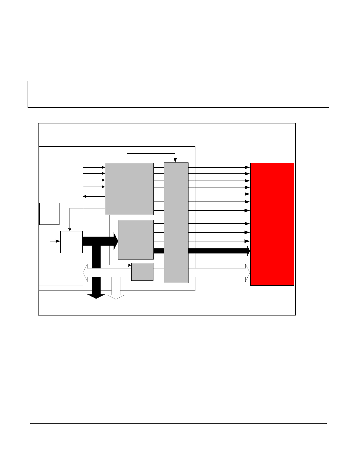
1 – Signal Chain of SDRAM
Figure 1 illustrates the signal chain between the ADSP-21161N, the controller and the SDRAM itself. The
3 parts for the signal flow to be considered:
• ADSP-21161N (core, DMA, address buffer)
• SDRAM Controller (command logic, address multiplexer, data buffer and clock divider)
• SDRAMemory
Figure 1: Signal chain: A DSP- 21 161 N t o S DRAM
ADSP-21161N
Core
DMA
CCLK
int. RD
int. WR
int. Reset
int. ACK
Address
buffer
busy
SDEMx
A27:0
A23:0
(non SDRAM)
m
o
C
A
SDBUF
D47:16
m
a
o
L
d
d
M
d
n
c
i
g
s
s
e
r
p
i
t
l
u
SDCKR
CCLK
SDCKE
~RAS
~CAS
~SDWE
DQM
SDA10
~MSx
A14
r
e
x
A13
e
l
A9:0,
A12:11
Data
buffer
Divider
Unit
CCLk
or
CCLK/2
max. 100 MHz
CLK
CKE
~RAS
~CAS
~WE
DQM
A10
SDRAM
~CS
BA0
BA1
A9:0,
A12:11
DQ31:0
2 – On-Chip Controller Architecture
The synchronous interface between the ADSP-21161N and the on-chip controller can be described in 3
basic parts:
2.1 – Command Logic
Because of the 2 different timing protocols, the internal SHARC commands are converted to comply with
the JEDEC standard for SDRAMs. The SDCLK clock, maximum 100 MHz, is used for synchronous
operation. The SHARC’s internal request lines or strobes are used to access the SDRAM with pulsed
The ADSP-21161 SHARC® On-chip SDRAM Controller (EE-163) Page 4 of 50
a
commands. The controller’s internal acknowledge signal inserts variable wait states to the DSP during
overhead cycles, caused by DRAM technology.
2.2 – SHARC Address Buffer
The SHARC’s address buffer enables the controller activation depending on bank assignment and external
address. The SHARC’s address pipeline depth is 1; therefore address pipelining is not supported.
2.3 – Address Multiplexer
Every first read or write action is issued in multiplexed mode. A maximum of 8192 Rows (13 addresses)
within 2048 columns (11 addresses) can be addressed. Furthermore, A[14:13] lines are used to select the
current SDRAM bank.
2.4 – Data Buffer
If systems incorporate a heavy busload, additional data buffers are used to decouple the input from the
capacitive load. The internal data buffer in conjunction with an external buffer reduce additional logic to a
minimum.
2.5 – Clock Divider
The clock divider unit controls the SDRAM with core or core half speed.
2.6 – I/O Capability
The system is designed to support up to 32-bit I/O over the external port. For code execution, the shared
linkports (I/O 16-bits) can be used to get a maximum I/O of 48-bit. The controller doesn’t know about the
connected I/O size.
2.7 – SDRAM Types
The interface supports various LVTTL SDRAMs depending on size and organization (I/O capability and
pages size).
Size I/O capability Page size
1M x 16 256
16-Mbits
2M x 8 512
4M x 4 1024
2M x 32 256
64-Mbits
4M x 16 256
8M x 8 512
16M x 4 1024
4M x 32 256
128-Mbits
8M x 16 512
16M x 8 1024
32M x 4 2048
256-Mbits 8M x 32 256
The ADSP-21161 SHARC® On-chip SDRAM Controller (EE-163) Page 5 of 50
a
d
d
d
d
d
d
16M x 16 512
32M x 8 1024
64M x 4 2048
2.8 – Control Registers
3 memory mapped register control the whole interface:
• Wait Register (access mode)
• SDRDIV Register (refresh counter)
• SDCTL Register (control of SDRAM controller and SDRAM)
3 – Command Coding
This chapter covers all kind of information related to control the SDRAM.
Note: All SDRAM commands are fully transparent to the user.
3.1 - Pin Description of Controller
For pin description of the interface ([1], pg.8-7)
3.2 - Controller Command Truth Table
This section provides a table to get an overview of all commands provided by the SDRAM controller.
Commands SDCKE sampled high
SDCKE(n-1) SDCKE(n) A[0-9,11-14] SDA10 ~MS[0-3] ~RAS ~CAS ~SDWE
MRS 1 1 Vali
ACT 1 1 Vali
RD 1 1 Vali
WR 1 1 Vali
Vali
Vali
0 0 0 0
0 0 1 1
0 0 1 0 1
0 0 1 0 0
DESL 1 1 X X 1 X X X
PREA 1 1 X 1 0 0 1 0
REF 1 1 X X 0 0 0 1
X=don’t care, 0=logic 0, 1=logic 1
These commands are handled automatically by the interface.
While the SDCKE line toggles in asynchronous manner, the commands are sampled synchronous to the
CLK signal.
Commands with Transition of SDCKE
SDCKE(n-1) SDCKE(n) A[0-9,11-14] SDA10 ~MS[0-3] ~RAS ~CAS ~SDWE
SREF En 1 0 X X 0 0 0 1
SREF Ma 0 0 X X X X X X
SREF Ex 0 1 X X 1 X X X
The ADSP-21161 SHARC® On-chip SDRAM Controller (EE-163) Page 6 of 50
a
r
d
X=don’t care, 0=logic 0, 1=logic 1, En=entry, Ma=maintain, Ex=exit
Note: Power-down, Suspend mode and auto precharge are not supported.
3.3 – Relevant Specs
Timing Spec Description Configuration Register
CCLK core clock 20-100 MHz peripheral
TREF row
TRAS active to precharge 1-15 cycles SDCTL
TRCD RAS to CAS delay 1-7 cycles SDCTL
TRP precharge to active 1-7 cycles SDCTL
TDRD dummy reads 2 + CL cycles Fixed
TRC(TRFC) row refresh cycle TRC=TRAS+TRP SDCTL
TMRD(TRSC) MRS to active 2 cycles Fixed
TXSR self- to auto refresh 2 + TRC cycles Fixed
CL read (CAS) latency 1-3 cycles SDCTL
3.4 - Simplified State Diagram
The state diagram is useful to analyze all deterministic sequences. Figure 4 shows all possible states:
efresh perio
0-0xFFFF SDRDIV
3.5 – Setup and Hold Times
The synchronous operation uses the SDCLK as reference. Commands, addresses and data are latched at
the rising edge of SDCLK. The valid time margin around the rising edge is defined as setup time (time
before rising edge) and hold time (time after rising edge) to guarantee that both the controller and the
SDRAM are working reliably together. Signal’s- slew rates, propagation delays (PCB) and capacitive
loads (devices) influence these parameters and should be taken into consideration [2].
The ADSP-21161 SHARC® On-chip SDRAM Controller (EE-163) Page 7 of 50
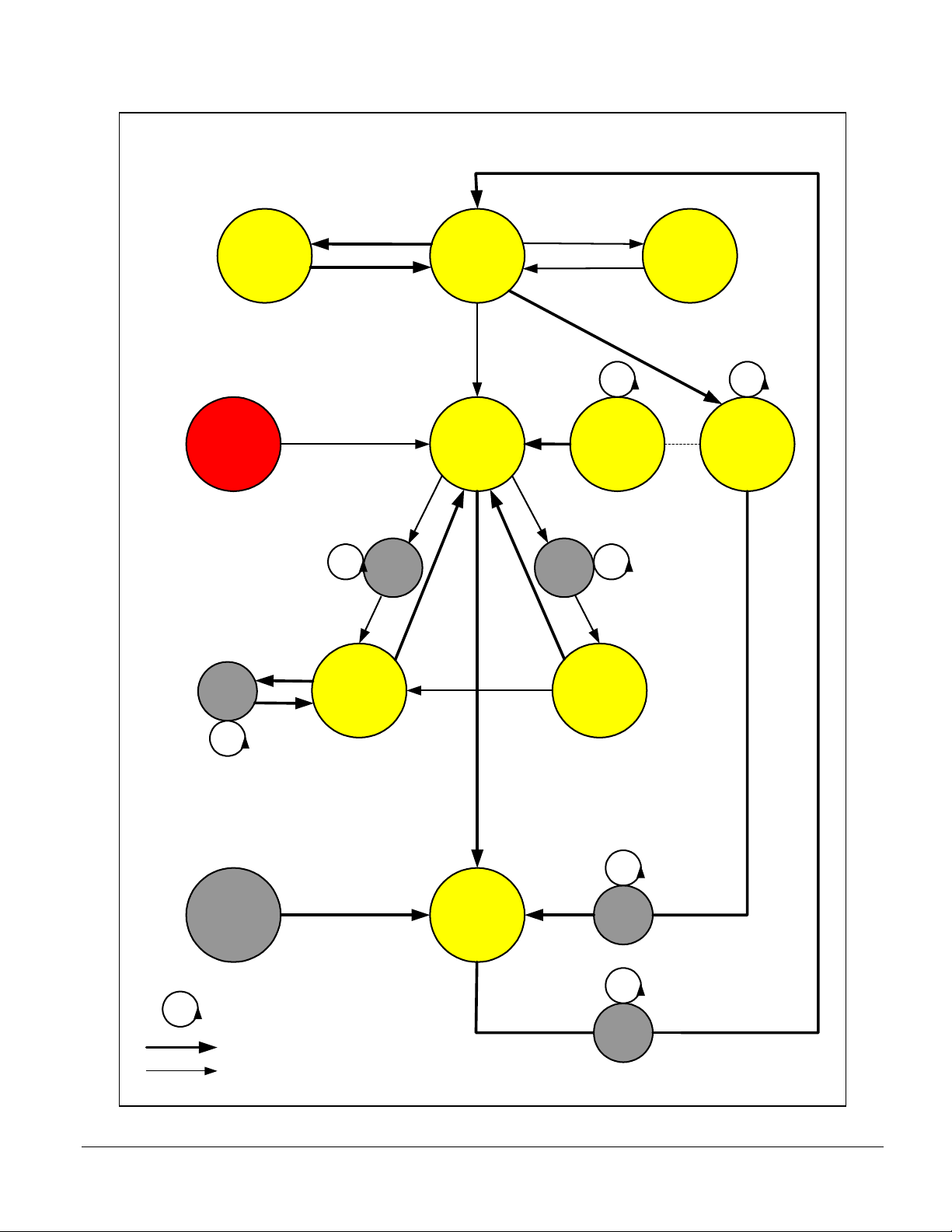
Figure 4: Simplified State Diagram: ADSP-21161N SDRAM Controller
a
Mode
Register
Core
IOP
MMS
Host
CL
1-3
MRS SREF
tMRD=2 tXSR=2+tRC
DESL
RD
tRCD
1-7
Single
Read
L
S
E
D
Idle
State
ACT
Row
activate
RD
DESL
WR
D
E
S
L
Exit
tRCD
1-7
Single
Write
REF
SDRDIV
Counter
expired
Self
Refresh
Auto
Refresh
PREA
Controller works in burst length 1
only one bank at the time
can be active
set bit
SDPSS in
IOCTL
Core Cycles, CL in SDCLK
Automatic sequence
User sequence
PREA
Pre-
charge
all
tRAS
1-15
tRP
1-7
The ADSP-21161 SHARC® On-chip SDRAM Controller (EE-163) Page 8 of 50
a
4 – Hardware Properties
The next properties apply for the ADSP-21161N:
4.1 – SDRAM Interface Speed Control
The pins CLKIN/XTAL, CLK_CFG[1:0] and ~CLKDBL affect the speed of SDRAM interface.
Additional, the SDCKR-bit influences the speed as well. The ID number must be 0 or 1 for an uniprocessor system, otherwise the SDCLK[0:1] are not driven (BSYN-bit / SYSTAT must be set). Next
table shows 12 different possibilities for speed configuration:
CLK_CFG1 CLK_CFG0 ~CLKDBL CLKIN:CCLK SDCKR-bit CLKIN:SDCLK
0 0 1 1:2
0 1 1 1:3
1 0 1 1:4
0 0 1 1:2
0 1 1 1:3
1 0 1 1:4
0 0 0 1:4
0 1 0 1:6
1 0 0 1:8
0 0 0 1:4
0 1 0 1:6
1 0 0 1:8
1 1:2
1 1:3
1 1:4
0 1:1
0 1:3/2
0 1:2
1 1:4
1 1:6
1 1:8
0 1:2
0 1:3
0 1:4
Different settings can result in the same speed for the SDRAM interface. Which settings are useful
depends on the used peripherals. The CLKOUT clock samples internal the SRAM, host, IRQs and IOFlags interfaces and are affected by the CLKIN input and ~CLKDBL pin, not the CLK_CFGx pins. ([2],
pg.20). This will help to balance the system and to find the best ratio between CLKOUT, Core clock and
SDRAM clock.
Note: The SDRAM interface is internally sampled with core cycles.
4.2 – SDRAM Clock Control
The SDRAM clock is provided by the DSP, not by an external clock oscillator. Even if the SDRAM
interface is disabled, the SDCLK0 and SDCLK1 are driven out of reset. You can vary the clock between
CCLK/2 or CCLK (SDCKR bit in SDCTL). The DSDCTL and DSDCK1 SDCTL control the SDRAM
clock pins.
DSDCK1 DSDCTL SDCLK0 SDCLK1 Comment
0 0 CCLK/2 CCLK/2 Both clocks active (reset value)
0 1 Hi-Z CCLK/2 SDCLK0 and control disabled, SDCLK1 enabled
1 0 CCLK/2 Hi-Z SDCLK0 and control enabled, SDCLK1 disabled
1 1 Hi-Z Hi-Z SDRAM Interface disabled
If SDRAM interface is not used, set both bits DSDCTL and DSDCK1 to 1, the bits SDEMx=000. This
allows the ~MSx banks to be used for other memory types.
The ADSP-21161 SHARC® On-chip SDRAM Controller (EE-163) Page 9 of 50
a
4.3 – SDRAM Address Space
All 4 ~MS[3-0] banks support SDRAM. As the external port supports 24 address bits, some restrictions
apply.
Bank V-Field A[26-27] E-Field A[21-23] Size Comment
0 00 111 62.68 Mwords Part of internal memory
1 10 000 64 Mwords
2 01 000 64 Mwords
3 11 000 64 Mwords
For bank 0, the controller issues external address starting at 0x200000, A[21]=1 to the SDRAM, but the
virtual addresses A[26:27] are still zeros. Addresses smaller 0x200000 are not accessible in bank 0 and
represent MMS and internal memory.
4.4 – Address Mapping Scheme
Basically, there are various possibilities accessing the SDRAM, for instance you access all rows in a bank
sequentially or you access all banks in a row sequentially. PC DIMM modules are accessed different by
its controller compared to a typical DSP application. The ADSP-21161 controller uses a hardware map
scheme optimized for digital signal processing ([1], pg.8-26).
Note: The address map scheme allows you to understand the system’s performance.
Two control bits (SDBN- and SDPGS-bits / SDCTL) are used to program the address map scheme for
different memory organizations. Figure 2 reproduces an example of the controller’s address mapping. In
page 0, the SDRAM’s banks A to D are sequentially selected. As bank interleaving is not supported, every
bank access in the same page has the overhead as an access between 2 pages. The address region of a full
page for instance 0x200000 to 0x2003FF (1024 words) can be accessed with 1 cycle/word.
The ADSP-21161 SHARC® On-chip SDRAM Controller (EE-163) Page 10 of 50
a
Figure 2: Controller Address Mapping to bank 0 of ADSP-21161N
4M x 4bit x 4, Page size 1024 words
Bank_A Bank_B Bank_C Bank_D
On Page
Access
g
a
P
e
g
a
P
0x200000
0x2003FF
0x200400
0
e
0x2FFF000
0x2FFF3FF
5
9
0
4
0x2007FF
Off Bank
Access
0x2FFF400
0x2FFF7FF
0x200800
0x200BFF
0x200C00
0x200FFF
Off Page
Access
0x2FFF800
0x2FFFBFF
0x2FFFC00
0x2FFFFFF
Note: Only one bank at a time can be active. Off-bank and off-page access have the same overhead.
4.5 – SDRAM Transfer Interruption
The pins CLK_CFG[1:0], ~CLKDBL and SDCKR-bit influence the SDRAM transfer interruptions. If
SDRAM accesses (reads or writes) are interrupted, the controller inserts stall cycles (DESL) to match with
the internal timing boundary based on CLKIN cycles ([1], pg.8-25).
4.6 – Interface during Reset
SDRAM interface status ([1], pg.13-20).
4.7 – Extended Precision
The PX-register allows core transfers of 40/48-bit to internal and external memory. This requires the
setting of IPACK-bit zero in SYSCON to enable 3 column accesses to SDRAM/SBSRAM or SRAM ([1],
pg.5-13).
The ADSP-21161 SHARC® On-chip SDRAM Controller (EE-163) Page 11 of 50

a
4.8 – Circular Access
The controller supports the circular buffer during core access for sequential read or writes in the whole
page, performing a throughput of 1 cycle/word in the boundary.
Note: This functionality is similar to the DAG’s circular buffering mode.
5 – Command Properties
5.1 – Mode Register Set (MRS)
The controller fixes following spec of SDRAM:
Burst length: one
Burst type: sequential
The controller uses no burst mode (burst length one) only. Every read or write command is accompanied
with an external address by the controller.
Note: every SDRAM vendor supports Burst length 1.
5.2 – Deselect (DESL)
Each SHARC bank ~MS[0-3] can be mapped in the memory region of the SDRAM. All 4 SHARC banks
can be connected (bit SDEMx / SDCTL) to the interface. The DESL command has the same functionality
as the NOPs; furthermore, next table lists the different situations in which the DESL occurs:
DESL truth table
• Non-external SDRAM access (access to another SHARC bank)
• Core access (e.g. computation unit, interrupt, cache, DAG)
• DMA operation (higher priority request of IOP)
• SDRDIV counter expired (refresh period counter)
• SDRAM read to write transition
• SDRAM off page and off bank access
• ~HBR asserted (host interface)
• ~BRx asserted (multiprocessing)
5.3 – I/O Mask Function (DQM)
It’s used to disconnect the SDRAM’s I/0 buffer to avoid data contention. The affect latency is zero cycles.
The truth table for DQM:
The ADSP-21161 SHARC® On-chip SDRAM Controller (EE-163) Page 12 of 50
a
SDCKE(n) DQM
MRS 1 1
ACT 1 0
RD 1 0
WR 1 0
DESL 1 0
PREA 1 1
REF 1 0
The controller simply disables the I/O buffer during MRS and PREA command.
Note: The controller does not support partial writes. Therefore, all DQM lines (e.g. DQMH and DQML)
should simply be tied together.
5.4 – SDRAM Bank Select
The controller uses the addresses 13 and 14 for the SDRAM bank selection. The next tables show the truth
table with SDA10, A14 and A13:
Banks A[13] A[14] SDA10
SDRAM with 2 banks
Bank_A - 0 0
Bank_B - 1 0
Both Banks - x 1
SDRAM with 4 banks
Bank_A 0 0 0
Bank_B 0 1 0
Bank_C 1 0 0
Bank_D 1 1 0
All Banks x x 1
x=don’t care, 0=logic 0, 1=logic 1
Note: A14 must be used for 2-banked memories.
Note: It doesn’t matter if you connect A[14:13] to BA[1:0] or A[14:13] to BA[0:1].
5.5 – SDRAM Address 10 (SDA 10)
It provides a special solution to gain refresh control about the SDRAM (without control of address bus) in
host mode. It must be connected with the SDRAM’s A10 pin. This pin has multifunctional character:
depending on the command, it acts as an address (MRS and ACT) or as a command (RD, WR and PREA).
Note: This pin replaces the DSP’s A10 pin during SDRAM accesses only.
5.6 – Write (WR)
Write operations do not use address pipelining. No stall cycles will be inserted.
The ADSP-21161 SHARC® On-chip SDRAM Controller (EE-163) Page 13 of 50

a
5.7 – Read (RD)
The SHARC architecture doesn’t support address pipelining. The next address will only be latched when
the previous data are driven off-chip. For sequential reads, the controller simply applies the command and
address assuming that it will be sequential. For non-sequential reads, it inserts additional dummy reads in
order to reject the data given out by SDRAM, if the next address from the core is non-sequential. It
applies to:
• Non sequential reads
• Sequential reads interruption
• Read to write transition
5.8 – Precharge All (PREA)
This command precharges all banks of the SDRAM simultaneously (SDA 10 high to select all banks),
which returns the banks in idle state.
Note: The controller doesn’t support precharge of single bank while only one bank at the time is active.
5.9 – Auto Refresh (REF)
The auto- or CAS before RAS- refresh requires only a command, no addresses. After the SDRAM
registers the command, it asserts internally CAS and delays RAS to execute a single row refresh. Up to 4
SHARC banks are simultaneously refreshed with ~MS[3:0].
Note: The controller doesn’t support burst refresh.
5.10 – Self Refresh (SREF)
The self-refresh is a very effective way to reduce the application’s power consumption to a minimum. The
device can run in this mode during long non-SDRAM operations. This mode is used to set the SDRAM
and SDRAM-controller in “stand-by”. The device starts refreshing itself triggered by an internal timer.
Additional, only this command allows the transition to another SDRAM controller during run-time.
6 – Shared Memory
This section covers the arbitration logic used to guarantee multiprocessing systems including SDRAM as
shared memory. The ADSP-21161N can be connected to a multi-processor cluster of six. Only one
SHARC can drive the bus at the time to the SDRAM. The interface works bi-directional (BSYN-bit /
SYSTAT set for ID=1-6) in order to detect commands MRS, REF and SREF and PREA. For systems with
heavy busload, you can use both clock outputs (e.g. SDCLK0 for LSB data and SDCLK1 for MSB data).
It is not allowed to use only SDCLK1 in a cluster system, because SDCLK1 is limited to an output
(unidirectional).
6.1 – MRS
Power up sequence can be done by any of six DSPs. Since broadcast write is not supported on ADSP21161N, all six DSPs must set the bit SDPSS/ SDCTL, the one which has the bus mastership, will do
power-up. The slaves recognize power-up with the MRS and clear its read-only SDPSS bit.
Note: For multiprocessing, the MRS is issued once.
The ADSP-21161 SHARC® On-chip SDRAM Controller (EE-163) Page 14 of 50

a
6.2 – REF
This detection helps to synchronize all six refresh counters. The slave’s SDRDIV counter will be
decremented each time the interface detects a refresh. This feature guarantees a periodic refresh and
requires the exact same settings of SDRDIV and SDCTL registers.
Note: For multiprocessing, the control settings must be identical for each DSP.
6.3 – SREF
This detection helps to synchronize the self-refresh base. The master’s bit SDSRF brings the whole
system in self-refresh mode. The slave recognizes the SREF and set therefore its bit SDSRF. The current
SDRDIV counters will be frozen until the self-refresh is exited.
6.4 – PREA
The BTC is used to arbitrate between the maximum of six controllers. Because the new SDRAM
controller doesn’t know which row in the SDRAM was accessed before busmastership, it only executes a
PREA if the previous had accessed SDRAM.
7 – Programming the SDRAM Interface
7.1 – Guideline
When programming the interface depends on the application: If you need it for storage of boot memory,
the initialization must be placed in the dedicated loader files to ensure proper booting. If you use memory
dynamically in your system for data storage, the init sequence can be placed in the user code.
The Interface is programmed in following order:
1. WAIT Register (wait states count)
2. SDRDIV Register (setting the row refresh period value)
3. SDCTL Register (contains programmable SDRAM control bits)
7.2 – Wait Register (Wait States)
For proper internal handshake between core/DMA and controller, make sure that the wait state count
EBxWS (WAIT register) is set to zero ([1], pg.A-77).
The memory access mode EBxAM (WAIT register) becomes regardless for SDRAM as it is defined with
the SDEMx-bit / SDCTL. The ACK signal should not be de-asserted during SDRAM and SBSRAM
accesses. ACK should only be de-asserted during SRAM accesses ([1], pg.7-41).
7.3 – Refresh Counter (SDRDIV)
This counter enables applications to coordinate the clock rate with the SDRAM’s required refresh rate.
The SDRDIV register is used to enter the row refresh period in number of core cycles calculated in the
equation.
Following specs are related to the vendor’s datasheet:
The ADSP-21161 SHARC® On-chip SDRAM Controller (EE-163) Page 15 of 50

a
TREF defines the maximum time for the row refresh period (time until the same row is refreshed again).
Typical values are 32 or 64 ms.
Refreshrate is the quotient from row refresh period/number of rows. The interval between two
subsequent rows is historically fixed to 15.625 or 7.8125 µs. it’s a good compromise between data access
time and the refresh reliability.
⎛
CCLKSDRDIV −−−⋅=−−−⋅=
⎜
⎝
tREF
∑
Rows
⎞
⎟
()
5CLtRPeRefreshrat CCLK5CLtRP
⎠
Note: Don’t mix up the specs TREF and TRC(TRFC). TRC describes the single row refresh cycle. TREF
describes the row refresh period.
The controller sets SDRDIV=0 during power-up. Hereby, the controller issues permanent refresh
commands within the tRFC period.
Note: If you configure SDRDIV to 0, the controller issues permanent REF with tRFC cycles.
7.4 – SDRAM Controller (SDCTL)
Figure 5: SDRAM's relevant s pecs
CLK
Col
NOP
PRE
NOP
ACT RDNOP
Row
Col
NOP
NOP
NOP
CMD
ADDR
ACT WRNOP
Row
Data
tRCD
D
tRAS
tRC
tRP
CL
Q
In order to support timing requirements and power up modes for different SDRAM vendors, the ADSP21161N provides explicitly programmability of tRAS, tRP, tRCD and CL in the SDCTL register.
Following specs are related to the vendor’s datasheet:
The SDTRP bit defines the minimum precharge time TRP. It is executed every time a row will be closed.
The SDTRAS bit is used to define the minimum row active time TRAS. It is used during REF to drive the
single row refresh cycle by using the equation TRC=TRAS+TRP.
The SDTRCD bit is used to define the minimum RAS to CAS delay time TRCD. Every first access in a
new row will decrement the TRCD counter before the read or write occurs.
The ADSP-21161 SHARC® On-chip SDRAM Controller (EE-163) Page 16 of 50

a
The SDCL bit is used to define the minimum Read (CAS) latency. Read Latency depends on the
application’s speed and different speed grades of devices. CL is the most critical parameter to be set.
Nowadays, some manufacturers don’t support a CL=1. The threshold for CL=1 is typically < 33 MHz. If
CL=1 is not specified in the datasheet, use CL=2, as CL=1 is not tested for the device (or contact
manufacturer). CL=2 is mostly used for speed < 100MHz as CL=3 valid for speed > 100 MHz.
Note: Higher settings cause a degradation of performance only.
The SDCKR bit allows applications to run the SDRAM with core or half core speed.
Depending on this, the specs SDTRP, SDTRAS, SDTRCD and SDRDIV must be doubled in count as they
are always sampled in core cycles. This does not apply to SDCL, as always sampled in SDCLK cycles.
Spec in cycles SDTRAS SDTRP SDTRCD SDRDIV SDCL
Sampling clock Core Core Core Core SDCLK
SDCKR=1 x1 x1 x1 x1 x1
SDCKR=0
The SDPM bit controls 2 different power-up options:
SDPM=0 SDPM=0 Description for SDPM=0
PREA PREA brings the SDRAM in the defined idle state
8 REF MRS charges SDRAM’s internal nodes
MRS 8 REF initializes the SDRAM’s working mode
Note: Some vendors don’t stick to the power up sequence.
x2 x2 x2 x2
x1
7.5 – SDRAM (SDCTL)
Setting the SDPSS bit implicitly programs the SDRAM. During this scenario (MRS), the burst-length, type and Read latency are transferred. The execution of MRS requires a hardware reset.
Addresses Spec
A[6:4] Read Latency: 1-3 SDCLK cycles
Note: The SDRAM is implicit programmed during the MRS over the address bus.
Note: Up to 4 SDRAMs can be powered up simultaneously (~MS3-0).
7.6 – Reprogramming
The SDCTL register can be directly modified during run time but under following conditions: All settings
of SDCTL can be changed and influence the controller’s state machine directly. The only exception is the
power-up sequence (MRS). In other words, if you want to change the read latency, a hardware reset is
required. So, it is general possible to change the specs TRAS, TRP, TRCD or the dynamic memory bank
selection SDEMx during run time, but care will be taken in order to violate specs.
The ADSP-21161 SHARC® On-chip SDRAM Controller (EE-163) Page 17 of 50

161N
HW-
Reset
a
Figure 5: The Initialization and power up mode (PREA-REF-MRS)
required to start
power up mode
SDCKE
SDCLK0
~MSx
DQM
SDA10
ADDR
CMD
Controller
Initialization
start of power
VDD, VDDQ and
clock stable
Command decoder
disabled
1. Hardware
up sequence
2. Controller
Self refresh enabled
SDRAM's command
decoder enabled
DQ Buffer enabled
A0-11
8 x REF
REF
tRP tMRD
8 x tRCmin
3. SDRAM
REFPREA NOP MRS NOP ACT
SDRAM
Initialization
start normal
operation
Note: Only Zero Wait states will guarantee the correct internal acknowledge of the SDRAM controller to
the SHARC.
8– Timing Power up Sequence
The whole procedure (figure 5) is executed in 3 steps:
8.1– Hardware
After hardware reset of the ADSP-21161N, the SDCLK clock and the SDRAM’s power supply pins VDD
(core) and VDDQ (I/O) must provide a stable signal for a typical minimum time of 200µs. After this time
is elapsed, the SDCTL register can be accessed.
Note: If you don’t meet this requirement, the SDRAM will not work properly.
8.2 – Controller
The ADSP-21161N reads SDCTL settings and stores them for its state machine. Thus it enables first the
command decoder as soon as the dedicated ~MSx lines are asserted.
The ADSP-21161 SHARC® On-chip SDRAM Controller (EE-163) Page 18 of 50

a
8.3 – SDRAM
The bit SDPSS in SDCTL starts the power up sequence. Depending on the settings, the power up
sequence starts with its first command PREA. According to this, the DQM line keeps asserted while still
disabling the SDRAM’s I/O buffer. Finally after the MRS, the devices are ready for normal operation.
Moreover, the controller de-asserts the DQM line to enable the SDRAM’s I/O buffer. Now, the user can
access the device properly.
8.4 – External Buffering Access
Do not write to non-external SDRAM bank directly after starting the power-up sequence with SBUF bit
set. Normally, the controller interrupts the on going access for the MRS. But in this case, pipelining for
control and data are enabled and the controller cannot control the external address bus. Polling the DQM
pin will help to recognize the power-up end.
The first SDRAM data access occurs after:
Taccess = TRP + (8 x (TRAS+TRP)) + TMRD (SDCLK cycles)
Example:
CCLK=100MHz
TRAS=5
TRP=2
TMRD=2
Taccess = 2 + (8 x 8) + 2 = 68 SDCLK cycles or 680 ns
Note: In order to initialize properly the SDRAM, the first access to itself is delayed with the int. ACK until
the power up sequence has finished.
8.5 – Host Access
If the SHARC has answered with ~HBG to a host request ~HBR, it will start working in host mode
(HSTM-bit / SYSTAT). In host mode, only IOP registers of the SHARC (figure 6) can be accessed. The
direct SDRAM access via DMA is not possible, while the SDRAM’s addresses are not accessible. But to
keep the SDRAM’s information during host access, the controller issues REF with the help of SDA10.
The ADSP-21161 SHARC® On-chip SDRAM Controller (EE-163) Page 19 of 50

Figure 6: Host to ADSP-21161N
a
ADSP-21161N
CCLK
int. RD
int. WR
int. Reset
int. ACK
Core
DMA
Address
buffer
busy
SDEMx
A8:0
o
C
SDBUF
D47:16
m
m
L
d
A
M
d
n
a
g
o
e
r
d
l
u
SDCLK
SDCKE
c
i
~SDWE
s
s
x
e
l
p
i
t
A12:11
buffer
SDCKR
~RAS
~CAS
DQM
SDA10
~MSx
A14
r
e
A13
A9:0,
Data
Divider
Unit
CCLk
or
CCLK/2
max. 50/100 MHz
CLK
CKE
~RAS
~CAS
~WE
DQM
A10
~CS
SDRAM
If a host request (~HBR=0) occurs during power-up sequence, it will be interrupted. A useful workaround
by setting the bus-lock feature (BUSLK bit / MODE2) makes power-up indivisible.
Note: In host mode, the interface continues to drive the lines. In multiprocessing, the slaves are sampling
the lines.
9 – DMA Transfers
9.1 – Internal Memory and SDRAM
Since the SDRAM is mapped to any of the SHARC memory banks, it can be externally accessed as source
or destination for a DMA transfer. Only the master mode DMA can transfer data between SDRAM and
internal memory.
In this mode, the I/O Processor initiates transfers up to 400 Mbyte/s for 32-bit.
DMA Mode SDRAM Support
Master Yes
Paced Master No
Slave No
Handshake No
External Handshake No
The ADSP-21161 SHARC® On-chip SDRAM Controller (EE-163) Page 20 of 50

a
9.2 – Host and SDRAM
There is no glueless solution to transfer data directly between a host and the SDRAM using the autorefresh time base. The SDRAM will be continuously controlled by the DSP. The user should start 2 DMA
transfers via the SHARC’s internal memory:
1. Slave DMA, Host to internal memory
2. Master DMA, Internal memory to SDRAM
10 – Examples ADSP-21161N EZ-KIT Lite™
10.1 – Jumper Settings
The DSP is configured with the default ID=0.
With the 25 MHz oscillator on CLKIN, 100 MHz core speed is configured with JP21:
JP21 Setting value
1-2 ~CKKDBL Open
3-4 CLK_CFG0 Open
5-6 CLK_CFG1 Closed
The JP1 has an affect on the I/O capability of the SDRAM interface.
JP1 Setting Value
x32 Open
x48 Closed
It is important to remove JP22 (~BMS enable). It will disconnect the FLASH, which is programmed by
factory. Otherwise, the SDRAM interface is powered up by factory settings.
10.2 – Configuration 1
System Requirements:
Type: 1Mx16bit
Size: 2x (1Mx16bit) = 1Mx32bit
Core clock: 100 MHz
Use SDCLK0 only
No buffering mode
Connected to ~MS0
SDRAM Requirements:
Speed grade: 7, 2-banks, 256 words page, refreshrate = 64ms/4096
SDRAM clock: 100 MHz
SDCKR-bit = 1
Power up mode: PRE-8xREF-MRS, No self-refresh mode
SDTRAS = 44/10ns = 5
The ADSP-21161 SHARC® On-chip SDRAM Controller (EE-163) Page 21 of 50

a
SDTRP = 20/10ns = 2
SDTRCD = 20/10ns = 2
SDCL = 2 cycles @100MHz
SDRDIV = (100MHz*64ms/4096) – 9 = 1554d = 0x612
// asm module
#include “def21161.h”
init_SDRAM:
ustat1=dm(WAIT);
bit clr ustat1 EB0WS;
dm(WAIT)=ustat1; // 0 Wait states for bank 0
ustat1=0x612;
dm(SDRDIV)=ustat1; // Refresh Counter
ustat1=0x0221425A;
dm(SDCTL)=ustat1; // SDRAM Control
rts;
10.3 – Configuration 2
System Requirements:
Type: 1Mx16bit
Size: 2x (1Mx16bit) = 1Mx32bit
Core clock: 100 MHz
Use SDCLK0 only
No buffering mode
Connected to ~MS0
SDRAM Requirements:
Speed grade: 7, 2-banks, 256 words page, refreshrate = 64ms/4096
SDRAM clock: 50 MHz
SDCKR-bit = 0
Power up mode: PRE-8xREF-MRS, No self-refresh mode
SDTRAS = 44/10ns = 5*2 = 10
SDTRP = 20/10ns = 2*2 = 4
SDTRCD = 20/10ns = 2*2 = 4
SDCL = 2*1 = 2 cycles @100MHz
SDRDIV = (100MHz*64ms/4096) – 11 = 1552d = 0x610
// asm module
#include “def21161.h”
init_SDRAM:
ustat1=dm(WAIT);
bit clr ustat1 EB0WS;
dm(WAIT)=ustat1; // 0 Wait states for bank 0
ustat1=0x610;
dm(SDRDIV)=ustat1; // Refresh Counter
ustat1=0x040144AA;
The ADSP-21161 SHARC® On-chip SDRAM Controller (EE-163) Page 22 of 50
dm(SDCTL)=ustat1; // SDRAM Control
rts;
11 – Code Execution from SDRAM
Figure 7: Signal flow for code execution from SDRAM
a
PMD 47:0
Cache
32x 48 bit
Program
Sequencer
Instruction Clock
PMA
23:0
log ical
address
External Port
Address-
Translation
Mux
Packing
1:1, 1:2, 1:3, 1:6
Data
Packing
A14:0
physical
address
RD
SDRAM
48/32/16/8 bit
max.
DQ47:0
SDCLK
The figure 7 demonstrates the signal flow for code execution from SDRAM. The Program sequencer
issues a 24-bit address to the packing address translator followed by the controller’s input. The
controller’s multiplexed addressing operation reads a dedicated location in the SDRAM. Various packing
modes for code execution can be configured. Since data packing and latency cycles slow down the
dataflow, the sequencer receives the 48-bit opcode of the issued address some cycles delayed.
Note: The sequencer’s 24-bit address allows program execution in external bank 0 only.
11.1 – Hardware
As the external port of the ADSP-21161N is 32 bits, every instruction execution from SDRAM requires at
least 2 fetches from the sequencer. Unpacking allows transferring physical addresses (SDRAM) to logical
addresses (program sequencer) to generate a 48-bit large instruction word. If your application doesn’t use
the two link ports, the sequencer can directly fetch instructions from a 48 bit wide memory with packing
disabled. The IPACK bits in SYSCON select 48:48, 32:48, 16:48 and 8:48 ([1], pg.5-97). The data are
unpacked that they can properly fetched by the sequencer ([1], pg.5-100).
The ADSP-21161 SHARC® On-chip SDRAM Controller (EE-163) Page 23 of 50

a
Note: Don’t mix up external code execution packing (IPACK, SYSCON) with DMA packing for SWOverlays (HBW, SYSCON) and (PMODE, DMACx).
11.2 – Simulator/Loader
The tool’s linker description file (.LDF) is used to pack the individual instructions correctly during the
compilation into the physical memory segments. The memory segment’s logical address room must be
declared to the physical width. Doing this, the linker uses implicit byte order packing for the dedicated
section. Before the external instructions are fetched, the appropriate IPACK bit must be set ensure correct
simulation.
The program must place a jump to the first address of the dedicated segment for code execution. This does
not apply for “no boot mode”. After booting the DSP, the sequencer starts fetching the first portions of the
instruction.
// LDF-file for simulator and loader
Memory
{
bk0_pmco { TYPE(PM RAM) START(0x00200000) END(0x0020FFFF) WIDTH(32) }
}
SECTIONS
{
bk0_pmco
{
INPUT_SECTIONS($OBJECTS(bk0_pmco))
} > bk0_pmco
}
11.3 – Emulator
The emulator session handling is different. Doing this, the emulator uses an explicit PACKING command
for the correct byte order depending on the IPACK bit setting. Before downloading code to the target with
the emulator, the target options must be selected to “do not reset before downloading code”. The packing
command allows various packing modes [3]. The header file “packing.h” is provided by the tools. Before
the external instructions are fetched, the appropriate IPACK bit is set to ensure correct fetching. If using
no packing mode, the data bits 15-0 must be enabled (IPACK) before the downloading stream.
The program must place a jump to the first address of the dedicated segment for code execution. This does
not apply for “no boot mode”. After booting the DSP, the sequencer starts fetching the first portions of the
instruction.
// LDF-file for emulator
Memory
{
bk0_pmco { TYPE(PM RAM) START(0x00200000) END(0x0020FFFF) WIDTH(32) }
}
SECTIONS
The ADSP-21161 SHARC® On-chip SDRAM Controller (EE-163) Page 24 of 50

a
{
bk0_pmco
{
INPUT_SECTIONS($OBJECTS(bk0_pmco))
PACKING(6 B1 B2 B3 B4 B0 B0 B0 B0 B5 B6 B0 B0)
} > bk0_pmco
}
Note: For default 32:48 packing debug, the “tree column memory” of tools displays the logical address of
the sequencer; the “two column memory” displays the physical address.
11.4 – Packing Effects
It is important to distinguish now between logical and physical addresses: the logical address is executed
by the program sequencer, the physical addresses is the external memory location of code. Based on
various packing modes, the logical and physical address will differ (except no packing mode.)
Next table demonstrates the influence of instruction packing:
Due to the packing modes, the scheme limits the size of the internal contiguous program segments ([1],
pg.5-105). Using multiple segments, the program can incorporate jump instructions towards the end of
individual segments.
Contiguous program segments depending on packing:
Packing Mode Segment
No packing 62.68 Mwords
1:2 1 Mwords
1:3 0.5 Mwords
1:6 0.25 Mwords
Next table illustrates the influence of logical page size (program sequencer) and physical page size
SDRAM:
The ADSP-21161 SHARC® On-chip SDRAM Controller (EE-163) Page 25 of 50

Logical vs. physical addresses, default packing (32:48)
(bank 0,1M x 32bit, Page size 256 words)
a
Page
Access
logical address
Bank_A Bank_B
0x200000
0x20007F
Off Bank
Access
0x200100
0x20017F
0x200080
0x2000FF
Off Page
Access
0x200180
0x2002FF
0
ge
a
P
1
ge
a
P
physical address
Bank_A Bank_B
0x200000
0x2000FF
Off Bank
Access
0x200200
0x2002FF
0x200100
0x2001FF
Off Page
Access
0x200300
0x2003FF
Mode Logical addresses for same physical page size
No packing Page size
Packing 1:2 Page size / 2
Packing 1:3 Page size / 4
Packing 1:6 Page size / 8
In other words, the sequencer reads only 32 addresses (packing 1:6) to execute the first page miss for a
256 words SDRAM.
Next formula illustrates the relation between physical and logical addresses:
Logical vs. physical addresses, default packing (32:48)
(bank 0,1M x 32bit, Page size 256 words)
Page
Access
logical address
Bank_A Bank_B
0x200000
0x20007F
Off Bank
Access
0x200100
0x20017F
0x200080
0x2000FF
Off Page
Access
0x200180
0x2002FF
0
ge
a
P
1
ge
a
P
physical address
Bank_A Bank_B
0x200000
0x2000FF
Off Bank
Access
0x200200
0x2002FF
0x200100
0x2001FF
Off Page
Access
0x200300
0x2003FF
The ADSP-21161 SHARC® On-chip SDRAM Controller (EE-163) Page 26 of 50

a
No packing physical addresses = logical address
Packing 1:2 2 physical addresses = (logical address x 2) – (Start logical address)
Packing 1:3 4 physical addresses = (logical address x 4) – (3x Start logical address)
Packing 1:6 8 physical addresses = (logical address x 8) – (7x Start logical address)
e.g: 4 physical addresses = 0x2000FF * 4 – 3* 0x200000 = 0x2003FC, 0x2003FD, 0x2003E and
0x216203 (zero)
If packing enabled, the external memory’s physical address space requires 2-8 times as much space as the
program sequencer’s logical space.
11.5 – Instruction Pipeline
The next code extract will be analyzed (default packing 32:48):
logical physical Instruction
200000: 200000 bit set FLAGS FLG0; */ instr. 1 */
200001
200001: 200002 bit clr FLAGS FLG0; */ instr. 2 */
200003
200002: 200004 next instr; */ instr. 3 */
200005
Figure 8: the instruction pipeline for sequential code, Packing 32:48 (default)
Instruction
cycles
SDCLK
CMD
ADDR
OPCODE
FLAG0
ACT
Row
instr. 1 instr. 2 instr. 3 instr. 4
fetch
RD
47:16 15:0 47:16 15:0
decode execute
Pipeline
6 cycles
RD RD
Col
tRCD
1cycle
RD RD RD RD
Col Col Col Col Col Col Col
47:16 15:0
CL
2 cycles
instr. 1
RD
instr. 2
47:16 15:0
execute
The first instruction (figure 8) gets executed after roughly 10 cycles. To understand this number, the
following sequence has to be considered:
The ADSP-21161 SHARC® On-chip SDRAM Controller (EE-163) Page 27 of 50

a
1st step: the program sequencer sends a row activation command to the SDRAM.
nd
2
step: the column is opened with the period of time tRCD, e.g. 1 cycle.
rd
3
step: the data are valid within the CAS latency, e.g. 2 cycles.
th
4
step: in order to execute an instruction, the 3 level pipeline has to be filled. The 1st instruction gets
fetched, decoded (meanwhile the 2
instruction gets decoded), within 2 cycles each.
This adds up to the complete delay of the first instruction: tRCD+CL+6 cycles. From here on every
instruction of straight line code (SDRAM in sequential address order) gets executed every 2 cycles, since
the pipeline is filled.
The best case is shown in figure 9: no packing is required and the instruction can be executed in the 6
cycle. The next table gives an overview of the pipline delay depending from the packing mode:
Figure 9: the instruction pipeline for sequential code, no Packing 48:48
Instruction
cycles
nd
Instruction gets fetched) and then executed (same time the 2
th
SDCLK
CMD
ADDR
OPCODE
FLAG0
instr. 1 instr. 2 instr. 3 instr. 4
ACT
Row
RD
Col
tRCD
1cycle
RD RD
Col Col Col
CL
2cycles
RD
47:0 47:0
fetch
decode execute
Pipeline
3 cycles
47:0 47:0
Packing Timing spec Pipeline delay cycles
48:48 tRCD + CL + 3 6
32:48 tRCD + CL + 3x2 9
16:48 tRCD + CL + 3x3 12
8:48 tRCD + CL + 3x6 21
Note: tRCD= 1, CL=2, SDCLK cycles
The ADSP-21161 SHARC® On-chip SDRAM Controller (EE-163) Page 28 of 50

a
11.6 – Sequential Code crossing Page/Bank
This mode describes a sequential code, which exceeds the page or the bank. As the code is sequential, the
pipeline is not flushed in order to lose performance. Stall cycles are inserted for the following:
• Precharging the current page or bank
• Activation of the new page or bank
Note: Take the overhead into consideration while crossing between pages or banks of SDRAM.
11.7 – Non Sequential Code same Page/Bank
Interrupt service routines or subroutines require non-sequential addressing. With the help of delayed
branch instruction (db), there is a possibility to reduce the bottleneck as much as possible using the
jump(db) or call(db) instructions. The pipeline doesn’t have to be flushed; because the two
delayed instructions are executed in 4 SDCLK cycles before the jump or call. This fact improves the
performance by 4 SDCLK cycles compared to non-delayed branches. For non delayed branches:
• Flush the pipeline
• Fill the pipeline
11.8 – Non Sequential Code different Page/Bank
When the code jumps between different pages or banks, additional terms should be taken into
consideration: the pipeline must be flushed which adds extra cycles to the procedure:
• Flush the pipeline
• Precharge the current page or bank
• Activate the new page or bank
• Fill the pipeline
Note: This sequence builds the worst case for stall cycles.
12 – Loop Execution from SDRAM
Basically, single instruction loops are analyzed to figure out the controller’s loop handling
12.1 – Single Loop with DM Data Access
In this mode, the sequence must be interrupted, since the addressing mode is not sequentially built. For
each loop iteration, the controller performs the sequence listed in figure 10: The first two accesses fetch
the instruction in the first iteration, 4 dummy reads are inserted to interrupt the burst. The next iteration
fetches the instruction again. Thus, every iteration requires 6 SDCLK cycles per loop.
12.2 – Single Loop with PM Data Access, Cache enabled
Just like DM data access, (figure 10): but since the sequencer checks for the fetched instruction in the
cache (core access), every iteration requires 8 SDCLK cycles per loop iteration. In case of cache hits, the
instructions are executed with 1 cycle/word in the core.
The ADSP-21161 SHARC® On-chip SDRAM Controller (EE-163) Page 29 of 50

a
12.3 – Single Loop with PM Data Access, Cache disabled
This mode is basically same to the PM data access with one difference that every instruction is executed
from SDRAM and takes 8 SDCLK cycles per iteration.
Figure 10: Loop Iteration Handling: pm-access vs. dm-access
Packing 32:48, CL=2 cycles
Instruction
cycles
SDCLK
CMD
SDRAM
ADDR
Instr
CMD
Iteration N
RD RD
Col
Col Col Col
Q Q+1
Iteration N Iteration N-1
tDRD
RD RDRD
DESLRD DESL
loop iteration with
pm data access
tDRD
RD RDRD RD RD RD
RD
RD
Iteration N-1
RD
RD
change between
SDRAM and core
Q Q+1
DESL used to
accesses (cache)
SDRAM
ADDR
Instr
Col Col Col Col
loop iteration with
dm data access
Q Q+1 Q Q+1
Example: single pm data loop
logical physical Instruction
200000: 200000 bit clr FLAGS FLG0;
200001
200001: 200002 lcntr=4, do (pc,1) until lce;
200003
200002: 200004 f12=f12+f8,pm(i8,m8)=f12; /* cached */
200005
200003: 200006 bit clr FLAGS FLG0; /* cached */
200007
200004: 200008 f10=f4*f6; /* cached */
200009
200005: 20000A next instr;
20000B
In the code example, the controller fetches the instructions at PM address 0x200000 and 0x200001
(SDRAM addresses 0x200000-0x200003). Address 0x200002 (SDRAM addresses 0x200004, 0x200005)
The ADSP-21161 SHARC® On-chip SDRAM Controller (EE-163) Page 30 of 50

a
k
k
d
with pm access is loaded into the cache. The sequencer restarts with another read at the same address and
detects a cache hit. Each instruction is executed at a rate 1 cycle/word. The next-to-last iteration caches
0x200003 (SDRAM addresses 0x200006, 0x200007) again. The last iteration fetches 0x200004 (SDRAM
addresses 0x200008, 0x200009) and the loop execution has finished. This explains, why a single pm data
access loop with 3 iterations gives no advantage since the instructions are only cached and not executed.
From four iterations on, all additional iterations are executed from the cache, thus increasing performance.
12.4 – Code Execution Performance Overview
Following settings are used:
Silicon=ADSP-21161N Rev0.3
CLKIN=12 MHz
~CLKDBL=0, CLK_CFG[1:0]=00, SDCKR=1
Core/SDCLK=48 MHz
~MS0=zero wait states
Size=1Mx48-bit
SDRDIV=742 cycles
tRAS=2cycles
tRP=1cycle
tRCD=1cycle
CL=2 cycles
No buffering mode
Sequential Code
On page Off page/ban
Fill pipeline X TRCD+CL+6 10
Sequential crossing X TDRD+TRP+TRCD+2 8
Non-sequential Code
On page Off page/ban
Branch X TDRD+6 10
Branch(db) X TDRD+2 6
Branch X TDRD+TRP+TRCD+1+6 14
Branch(db) X TDRD+TRP+TRCD+1+2 10
Single instruction loop
Cache Cache disable
PM data X 1 upon 4
PM data X 8
DM data - - 6
Stall cycles Testcase
Stall cycles Testcase
Cycles/iteration
th
The ADSP-21161 SHARC® On-chip SDRAM Controller (EE-163) Page 31 of 50

a
4
10
3
10
SDCL K cycl es
2
10
1
10
0
10
Figure11: S i ngl e Instr. Loop i terat i ons vs. c ycles
10
1
loop iterat i ons
10
2
10
3
Figure 11 illustrates the following:
For high loop iterations, for instance 1000, the dashed line (pm, no cache) takes about 6000 cycles to
execute. The dash dot line (dm) takes about 5000 cycles. The best case gives of course the use of cache.
This results to 1000 cycles.
13 – Optimizing the Performance
13.1 – SDRAMs for Data Storage
The market doesn’t offer the combination of big page size (e.g. 1024 words) and a wide interface (32 bit),
which would be desirable for DSP applications. Parallel connection does the trick: the advantage of good
SDRAM performance for the price higher hardware requirements.
Note: All four SHARC banks support maximum 256M x 32bit.
The table below lists the possible configuration of different pages sizes creating a 32-bit I/O capability:
Note: In cases of high capacity load, you should use the buffering feature.
Size I/O capability Parallel Total Capacitance / pin SDBUF bit
1Mx16 2 (2 x pin SDRAM + PCB) No
16 Mbits
2Mx8 4 (4 X PIN SDRAM + PCB) Yes
4Mx4
8
(8 X PIN SDRAM + PCB) Yes
The ADSP-21161 SHARC® On-chip SDRAM Controller (EE-163) Page 32 of 50

a
64 Mbits
128 Mbits
256 Mbits
13.2 – SDRAMs for Code Storage
Execution of instructions directly from the SDRAM sharing the two link ports is possible. This no packing
mode allows best performance.
The table below lists the possible configuration of different pages sizes creating a 48-bit I/O structure:
Size I/O capability Parallel Total Capacitance / pin SDBUF bit
16 Mbits
64 Mbits
128 Mbits
256 Mbits
4Mx16 2 (2 x pin SDRAM + PCB) No
8Mx8 4 (4 X PIN SDRAM + PCB) Yes
16Mx4 8 (8
X PIN SDRAM + PCB) Yes
8Mx16 2 (2 x pin SDRAM + PCB) No
16Mx8 4 (4 x pin SDRAM + PCB) Yes
32Mx4 8 (8 X PIN SDRAM + PCB) Yes
16Mx16 2 (2 x pin SDRAM + PCB) No
32Mx8 4 (4 X PIN SDRAM + PCB) Yes
64Mx4 8 (8
X PIN SDRAM + PCB) Yes
1Mx16 3 (3 x pin SDRAM + PCB) No
2Mx8 8 (8 X PIN SDRAM + PCB) Yes
4Mx4
12
(12 X PIN SDRAM + PCB) Yes
4Mx16 3 (3 x pin SDRAM + PCB) No
8Mx8 8 (8 X PIN SDRAM + PCB) Yes
16Mx4 12 (12
X PIN SDRAM + PCB) Yes
8Mx16 3 (3 x pin SDRAM + PCB) No
16Mx8 8 (8 X PIN SDRAM + PCB) Yes
32Mx4 12 (12
X PIN SDRAM + PCB) Yes
16Mx16 3 (3 x pin SDRAM + PCB) No
32Mx8 8 (8 X PIN SDRAM + PCB) Yes
64Mx4 12 (12
X PIN SDRAM + PCB) Yes
13.3 – External Buffering
In parallel connection one address and control bus feeds all devices. In order to meet the timing
requirements, help against the capacitive load would be desirable. It is recommended to use this feature if
the capacitive load exceeds the nominal 30 pF/pin. Also, the controller provides 2 features to cope
with this situation:
• 2 clock out lines (SDCLK0/SDCLK1) sharing the clock load
• Set SDBUF bit to 1(SDCTL) inserts a delay buffer to allow address- and command pipelining
Note: The external buffer reduces the power dissipation but increases the pipeline effects.
The ADSP-21161 SHARC® On-chip SDRAM Controller (EE-163) Page 33 of 50

Figure x: Signal chain: External Buffering
a
ADSP-21161N
CCLK
int. RD
int. WR
int. Reset
int. ACK
Core
DMA
Address
buffer
busy
SDEMx
A23:0
o
C
SDBUF
D47:16
m
m
L
d
A
M
d
n
a
g
o
e
r
d
l
u
SDCLK
SDCKE
c
i
~SDWE
s
s
x
e
l
p
i
t
A12:11
buffer
SDCKR
~RAS
~CAS
DQM
SDA10
~MSx
A14
r
e
A13
A9:0,
Data
Divider
Unit
CCLK
or
CCLK/2
SDRAM
Register
DQ31:0
13.4 – SDRAM PC Modules
The maximum addressable size is 64Mx32-bit for each SHARC bank. The use of unbuffered (low load) or
registered (heavy load) DIMM modules is required but not so efficient (typical I/O sizes x32, x64 or x72bits), as the most vendors offer a size of x64-bits, which is commonly used for PCs. The SDRAM
controller can only handle a maximum of x32-bits.
Note: The ADSP-21161 supports 4 x (64M x 32bit) or 4 x 256Mbyte modules.
13.5 – Rules for Optimized Performance
Some rules to optimize the performance for external code execution:
• Try to find the best clock settings depending on CLK_CFG[1:0], ~CLKDBL and SDCKR-bit.
• If your application doesn’t need the link ports, you can execute 48-bit directly from SDRAM, which
gives the best performance
• Use straight line code for sequential SDRAM addressing if possible
• Use delayed branches instructions jump (db) and call (db) in a page instead of non delayed branches
• Remember the controller’s address mapping scheme, don’t mix up the logical- with physical
addresses.
The ADSP-21161 SHARC® On-chip SDRAM Controller (EE-163) Page 34 of 50

a
• Depending on the SDRAM’s pages size and number of banks, place your code segments to minimize
off page- and off bank accesses
• Use parallel connection for SDRAMs with big page size in order to obtain 48-32-16-8 bit (SDRAM:
the bigger the page size, the smaller the I/O structure)
• Use DM data access loops for loops with less than 6 iterations
• Insert dummy PM data access to utilize the cache performance of DM data access loops with more
than 6 iterations
• Use the SDRAM as code memory only, do not use it as data memory at the same time
• Use the optimized settings for the controller’s state machine (tRAS, tRP, tRCD, CL) depending on the
speed grade and on the application’s speed
14 – SDRAM and Booting
14.1 – Loader Kernel
When executing code or data storage from/to SDRAM, the code or data must be loaded in the device
before runtime. This requires an initialized SDRAM before downloading the code during the boot
scenario. The Tool’s loader provides this capability.
Boot loader sources and executables are available to boot from PROM, Host, SPI or Linkports.
Note: Independent from boot mode, the SDRAM must be initialized before the user’s application starts
writing data or code to it. This is possible during the 256-loader kernel words, otherwise the data will get
corrupted.
Next table summarizes the steps:
• 1. After ~RSTOUT de-asserted, the pins EBOOT, LBOOT, and ~BMS are sampled
• 2. Kernel (256 x 48 bit) is drawn down during hardwired DMA into the DSP (0x40000-0x400FF)
(~BMS or ~HBG continuously asserted)
• 3. Interrupt generation starts kernel execution, SDRAM and controller are initialized
(~MSx asserted for SDRAM setup)
• 4. User’s code and data are loaded into the DSP (0x40200-) or SDRAM with the help of TAGs
(~BMS, ~HBR, ~HBG and ~MSx are toggling requesting the bus)
• 5. Kernel is now overridden with user’s interrupt vector table
(~BMS or ~HBG continuously asserted)
• 6. DSP starts code execution at address 0x40005 or (0x200000, SDRAM)
Note: Do not violate the Initialization time, VDD, VDDQ and CLKIN and clock must be stable for typical
200 µs before SDRAM power up mode.
Note: The Tools allow the simulation of the boot process.
14.2 – Booting Modes
The boot mode is selected by hardware after reset. ([1], pg.13-70).
The ADSP-21161 SHARC® On-chip SDRAM Controller (EE-163) Page 35 of 50

a
14.3 – In Circuit Emulation (ICE)
During hardware debug sessions, you can quickly start the SDRAM controller with the emulator’s
software.
• First, push the hardware reset button
• Second, load an SDRAM_INIT.DXE file to start the SDRAM controller.
• Third, load the USERCODE.DXE file to start the SDRAM specific application.
Note: Only a hardware reset of ADSP-21161N can reinitiate the power up sequence for new settings.
Note: The Read Latency is fully transparent during single step debug sessions.
15 – Core and DMA Transfers to SDRAM
In this mode, the SDRAM is used as a source or destination for data transfers. To demonstrate the
performance, following settings are used:
Silicon=ADSP-21161N Rev0.3
CLKIN=12 MHz
~CLKDBL=0, CLK_CFG[1:0]=00, SDCKR=1
Core/SDCLK=48 MHz
~MS0=zero wait states
Size=1Mx48-bit
SDRDIV=742 cycles
tRAS=2cycles
tRP=1cycle
tRCD=1cycle
CL=2 cycles
No buffering mode
The ADSP-21161 SHARC® On-chip SDRAM Controller (EE-163) Page 36 of 50

15.1 – Sequential Reads without Interruption
a) Core reads from SDRAM, no interruption caused.
b) IOP reads (EMx=1) from SDRAM, no interruption caused.
Sequential uninterrupted Reads on Page
SDCLK
a
CMD
ADDR
DATA
~MS0
ACT
Row
tRCD
RD RD RD
Col
CL
RD
Col Col Col
QQ+1Q+2
Q+3
Nr. Cycles Core Controller Data
1 r1=dm(dest_Q); ACT
2 int. ACK RD
3 r2=dm(dest_Q+1); RD
4 r3=dm(dest_Q+2); RD Q
5 r4=dm(dest_Q+3); RD Q+1
6 RD Q+2
7 Q+3
The ADSP-21161 SHARC® On-chip SDRAM Controller (EE-163) Page 37 of 50

a
15.2 – Sequential Reads with minimum Interruption
a) Core reads from SDRAM, interruption caused by a core access.
b) IOP reads (EMx=1) from SDRAM, interruption caused by a higher priority request to IOP.
Sequential interrupted Reads
SDCLK
CMD
ADDR
DATA
~MS0
tRCD
ACTRDRDRD
Row
Col
CL
RD RD RD
Col Col Col Col Col
QQ+1Q+2 Q+3Q+4
tDRD
RD DESL DESL
Nr. Cycles Core Controller Data
1 r1=dm(dest_Q); ACT
2 int. ACK RD
3 r2=dm(dest_Q+1); RD
4 r3=dm(dest_Q+2); RD Q
5 int. ACK RD Q+1
6 int. ACK RD Q+2
7 int. ACK RD
8 int. ACK RD
9 int. ACK DESL
10 r5=r6*r7; DESL
11 r4=dm(dest_Q+3); RD
12 r5=dm(dest_Q+4); RD
13 r6=dm(dest_Q+5); RD Q+3
14 RD Q+4
15 Q+5
RD RD
The ADSP-21161 SHARC® On-chip SDRAM Controller (EE-163) Page 38 of 50

15.3 – Non Sequential Reads without Interruption
a) Core reads from SDRAM, no interruption caused.
b) IOP reads (EMx>1) from SDRAM, no interruption caused.
Nonsequential uninterrupted Reads on page
SDCLK
CL tDRDtRCD
a
CMD
ADDR
DATA
~MS0
ACT RDRD RD RD RD RD
Row Col Col
Q+3 Q Q+2
RD RD
RD RD
Nr. Cycles Core Controller Data
1 r1=dm(dest_Q+3); ACT
2 int. ACK RD
3 int. ACK RD
4 int. ACK RD Q+3
5 int. ACK RD
6 int. ACK RD
7 r2=dm(dest_Q); RD
8 int. ACK RD
9 int. ACK RD Q
10 int. ACK RD
11 int. ACK RD
12 r3=dm(dest_Q+2); RD
13 int. ACK RD
14 int. ACK RD Q+2
15 int. ACK RD
16 int. ACK RD
RD
Col
The ADSP-21161 SHARC® On-chip SDRAM Controller (EE-163) Page 39 of 50

15.4 – Sequential Writes without Interruption
a) Core writes to SDRAM, no interruption caused.
b) IOP writes (EMx=1) to SDRAM, no interruption caused.
Sequential uninterrupted Writes on Page
SDCLK
tRCD
a
CMD
ADDR
DATA
~MS0
ACT
Row
WR
Col
WR
Col Col Col
DD+1D+2
WR
WR
D+3
Nr. Cycles Core Controller Data
1 dm(dest_D)=r1; ACT
3 int. ACK WR D
4 dm(dest_D+1)=r2; WR D+1
5 dm(dest_D+2)=r3; WR D+2
6 dm(dest_D+3)=r3; WR D+3
The ADSP-21161 SHARC® On-chip SDRAM Controller (EE-163) Page 40 of 50
15.5 – Sequential Writes with minimum Interruption
a) Core writes to SDRAM, interruption caused by core access.
b) IOP writes (EMx=1) to SDRAM, interruption caused by a higher priority request to IOP.
Sequential interrupted Writes on Page
SDCLK
tRCD
a
CMD
ADDR
DATA
~MS0
ACT WR DESLWR WR
Row Col
Col Col Col Col
DD+1D+2
DESL
WR WR WR
Col
D+3 D+4 D+5
Nr. Cycles Core Controller Data
1 dm(dest_D)=r1; ACT
2 int. ACK WR D
3 dm(dest_D+1)=r4; WR D+1
4 dm(dest_D+2)=r5; WR D+2
5 r0=r0+1; DESL
6 int. ACK DESL
7 dm(dest_D+3)=r6; WR D+3
8 dm(dest_D+4)=r7; WR D+4
9 dm(dest_D+5)=r8; WR D+5
The ADSP-21161 SHARC® On-chip SDRAM Controller (EE-163) Page 41 of 50

15.6 – Non Sequential Writes without Interruption
a) Core writes to SDRAM, no interruption caused.
b) IOP writes (EMx>1) to SDRAM, no interruption caused.
Non sequential Writes on Page
SDCLK
tRCD
a
CMD
ADDR
DATA
~MS0
ACT WR WR WR
Row Col
D+1 D+3 D+5
Col Col ColCol
WR WR WR
Col
D+7 D+9
D+2
Nr. Cycles Core Controller Data
1 dm(dest_D+1)=r1; ACT
2 int. ACK WR D+1
3 dm(dest_D+3)=r4; WR D+3
4 dm(dest_D+5)=r5; WR D+5
5 dm(dest_D+7)=r6; WR D+7
6 dm(dest_D+9)=r7; WR D+9
7 dm(dest_D+2)=r8; WR D+2
The ADSP-21161 SHARC® On-chip SDRAM Controller (EE-163) Page 42 of 50

15.7 – Minimum Write to Read Interval
Core writes to and reads from SDRAM.
SDCLK
a
Write to Read on Page
CLtRCD
CMD
ADDR
DATA
~MS0
ACT
Row
WR WR WR RD
Col
Col Col Col Col Col
D D+1 D+2 Q Q+1 Q+2
RD RD
Nr. Cycles Core Controller Data
1 dm(dest_D)=r1; ACT
2 int. ACK WR D
3 dm(dest_D+1)=r1; WR D+1
4 dm(dest_D+2)=r1; WR D+2
5 r6=dm(dest_Q); RD
6 r6=dm(dest_Q+1); RD
7 r6=dm(dest_Q+2); RD Q
8 RD Q+1
9 RD Q+2
The ADSP-21161 SHARC® On-chip SDRAM Controller (EE-163) Page 43 of 50

15.8 – Minimum Read to Write Interval
Core reads from and writes to SDRAM.
SDCLK
CL tDRDtRCD
a
Read to Write on Page
CMD
ADDR
DATA
~MS0
ACTRDRDRD RD WR
Row Col Col
Col Col
RD RD RD
QQ+1Q+2 D
DESL DESL
DESL DESL WR
Nr. Cycles Core Controller Data
1 r1=dm(dest_Q); ACT
2 int. ACK RD
3 r1=dm(dest_Q+1); RD
4 r1=dm(dest_Q+2); RD Q
5 int. ACK RD Q+1
6 int. ACK RD Q+2
7 int. ACK RD
8 int. ACK RD
9 int. ACK DESL
10 int. ACK DESL
11 int. ACK DESL
12 int. ACK DESL
13 dm(dest_D)=r6; WR D
14 dm(dest_D+1)=r6; WR D+1
15 dm(dest_D+2)=r6; WR D+2
Col
D+1
The ADSP-21161 SHARC® On-chip SDRAM Controller (EE-163) Page 44 of 50

15.9 – Reads between Page/Bank
a) Core reads from SDRAM, interruption caused by another page or bank.
b) IOP reads (EMx=1) from SDRAM, interruption caused by another page or bank.
Sequential Reads between Pages or Banks
SDCLK
a
tDRD
DESL
tRP tRCD
Row
RD
Col Col
CMD
ADDR
DATA
DQM
SDA10
~MS0
CL
RD PREARD ACTRD
RD RD
Col
ColCol
Q
RD RD
Q+1 Q+2
Nr. Cycles Core Controller Data
1 r1=dm(dest_Q); ACT
2 int. ACK RD
3 r2=dm(dest_Q+1); RD
4 r2=dm(dest_Q+2); RD Q
5 int. ACK RD Q+1
6 int. ACK RD Q+2
7 int. ACK RD
8 int. ACK RD
9 int. ACK DESL
10 r2=dm(dest_Q+3); ACT
11 int. ACK RD
12 r2=dm(dest_Q+4); RD
13 r2=dm(dest_Q+5); RD Q+3
Q+3RDQ+4
The ADSP-21161 SHARC® On-chip SDRAM Controller (EE-163) Page 45 of 50

15.10 – Writes between Page/Bank
a) Core writes to SDRAM, interruption caused by another page or bank.
b) IOP writes (EMx=1) to SDRAM, interruption caused by another page or bank.
Sequential Writes between Pages or Banks
SDCLK
tRCD
tRP
a
CMD
ADDR
DATA
DQM
SDA10
~MS0
WR
WR WR WR WR WR
Col
D D+1 D+2
DESL
ColCol Col ColCol
PREA ACT
Row
D+3 D+4 D+5
Nr. Cycles Core Controller Data
1 dm(dest_D)=r1; ACT
3 int. ACK WR D
4 dm(dest_D+1)=r1; WR D+1
5 dm(dest_D+2)=r1; WR D+2
6 int. ACK DESL
7 int. ACK PREA
8 dm(dest_D+3)=r1; ACT
10 int. ACK; WR D+3
11 dm(dest_D+4)=r1; WR D+4
12 dm(dest_D+5)=r1; WR D+5
The ADSP-21161 SHARC® On-chip SDRAM Controller (EE-163) Page 46 of 50

a
15.11 – Refresh Sequence
The refresh counter triggers refresh requests. The figure shows the refresh sequence: In the first place, all
banks are precharged with SDA10 high and DQM high to avoid data conflict during precharge. The issued
refresh follows right away. During refresh, other commands cannot be executed. The ratio between
application time and refresh time is given by tRC=15.625µs/row:
e.g: 5 cycles/750 cycles x 100 = 0,66.
This means, the refresh sequence requires 0,66 % of the whole performance at 48 MHz. By reducing the
SDRDIV period, you can decrease the performance ratio to your needs.
Note: The auto refresh with 15,625 µs/row gives the best performance.
Auto Refresh Sequence @ 48 MHz
tRAS=2 cycles, tRP=1 cycle
SDCLK
CMD
SDRDIV counter
expired
SDA10
DQM
~MS3-0
DESL
REFPREA DESL
DESL
ACT
continue
normal
operation
Note: An REF command starts an internal row refresh with CAS before RAS. The ~MSx line is only
asserted if configured in the SDCTL register
The ADSP-21161 SHARC® On-chip SDRAM Controller (EE-163) Page 47 of 50

15.12 – Self Refresh
Figure above explains this sequence:
Self Refresh sequence
a
SDCLK
CMD
SDCKE
SDA10
DQM
~MS0
PREA
SREF
enter Self
refresh
clock
frozen
all inputs don't care
exept CKE
exit Self
refresh
DESL
tXSR
2 + tRC
cycles
DESL
REF
ACTDESL
normal
operation
When the application sets the SDSRF bit in the SDCTL register, the controller, in order to provide current
information, precharges all banks. During the PREA and the SREF command, the SDCKE transits from
high to low thus enabling the self-refresh mode. After entering, all the command inputs will get don’t care
status after one 1 cycle in order to reduce power consumption. Moreover the clock is frozen to reduce
power consumption as well.
An SDRAM access from the SHARC starts the controller, which ends the self-refresh function. The
SDCKE line transits high and the controller disables the command decoder for tXSR = 2+tRC cycles to
restart the refresh time base. After tRCmin, the device executes an auto refresh and starts normal operation
with the activate command after another tRCmin. The self-refresh mode is exited after:
tExit = 2*tRC + 2 (cycles)
Note: Only the SDCKE pin keeps control of the device in self-refresh mode.
The ADSP-21161 SHARC® On-chip SDRAM Controller (EE-163) Page 48 of 50
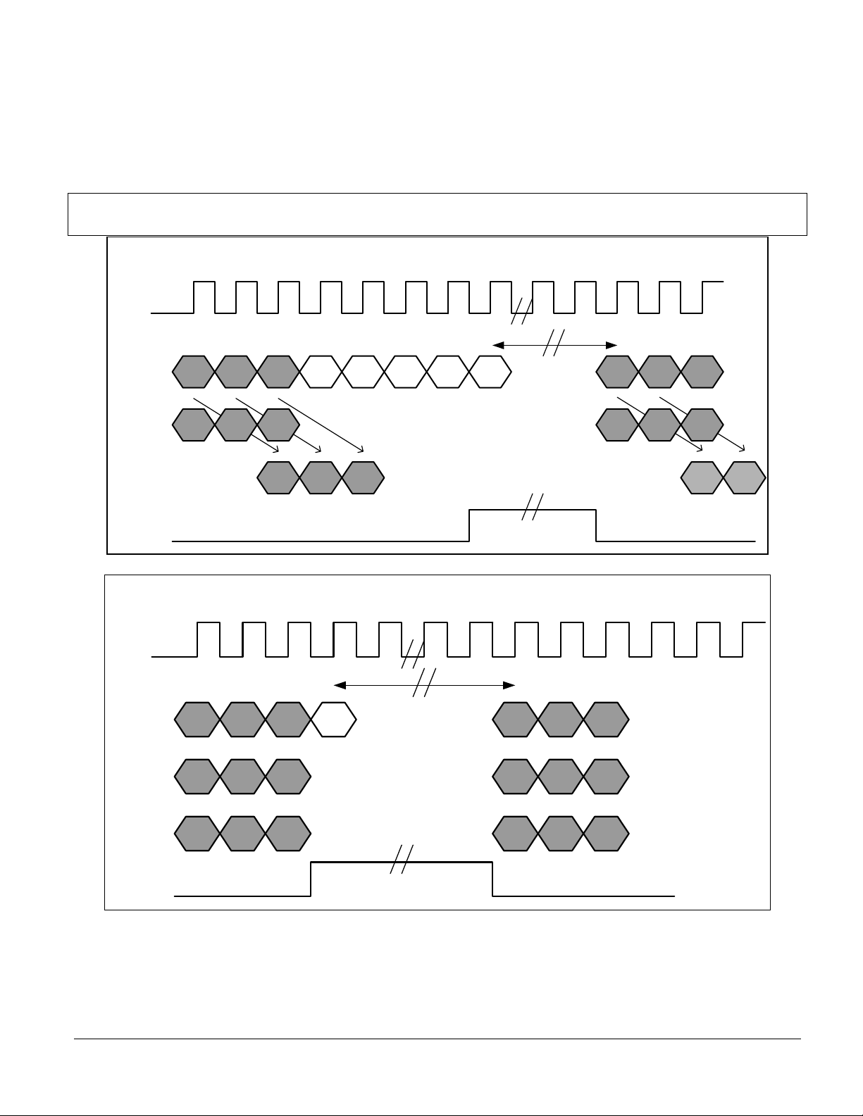
a
15.13 – Chained DMA Transfers
Loading the transfer control block (TCB) chain in between successive Master Mode DMA sequences. IOP
reads/writes (EMx=1) from/to SDRAM, no interruption caused by a higher priority request to IOP.
Read from SDRAM: 15 SDCLK cycles
Write to SDRAM: 17 SDCLK cycles
Chained DMA Reads
SDCLK
CMD
ADDR
DATA
RD RD RD RD
Col
Col Col
n-2 n-1 n n-a n-b
RD RD RD
DESL
15 cycles
for TCB
loading
RD RD
Col
Col Col
RD
~MS0
Chained DMA Writes
SDCLK
CMD
ADDR
WR NOP NOP
Col
ColCol ColCol
DESL
17 cycles
for TCB
loading
WR NOP NOP
Col
DATA
n-2 n-1 n
n-a n-b n-c
~MS0
The ADSP-21161 SHARC® On-chip SDRAM Controller (EE-163) Page 49 of 50

15.14 – Host access during Reads
SDCLK
~HBR
a
Host access during SDRAM Read
~HBG
CMD
ADDR
DATA
~MS0
RD RD
Col
RD RD
tDRD
RD
n n+1
DESL
DESL issu ed to g ra n t
the host access
DESL
DESL
RD
Col
RD
Col
A random host access during a read: After the detection of a request, the current operation of the SDRAM
controller is interrupted and frozen. After de-assertion of ~HBG, the controller continues driving the next
data.
Note: The current bus master in a cluster will drive the SDRAM interface (refresh) during ~HBG low. The
SDRAM bus master chip changes only with ~BRx in MMS.
Note: In host mode, the SDRAMs bank select lines A14 (BA0) and A13 (BA1) are not accessible. Only the
auto refresh command can be issued (SDA10).
References
[1] ADSP-21161N SHARC DSP Hardware Reference, 3rd edition, May 2002, Analog Devices Inc.
[2] ADSP-21161N DSP Microcomputer Datasheet, Rev.A, 2003, Analog Devices Inc.
[3] Linker and Utilities for SHARC DSPs, Rev.4, January 2003, Analog Devices Inc.
[4] ABC of SDRAMs (EE-126), April 2002, Analog Devices Inc.
Document History
Version Description
September, 2003 by Robert Hoffmann Updated chapters including VisualDSP++™ 2.0 to VisualDSP++ 3.0
March, 2002 by Robert Hoffmann Initial Release
The ADSP-21161 SHARC® On-chip SDRAM Controller (EE-163) Page 50 of 50
 Loading...