ANALOG DEVICES CN-0241 Service Manual

Circuit Note
ration to help solve today’s
AD7920
250 kSPS, 12-bit, 250 kSPS ADC in 6-Lead SC70
Rev. A
ts from Analog Devices have been designed and built by Analog Devices
engineers. Standard engineering practices have been employed in the design and construction of
room temperature. However, you are solely responsible for testing the circuit and determining its
suitability and applicability for your use and application. Accordingly, in no event shall Analog Devices
whatsoever connected to the use of any Circuits from the Lab circuits. (Continued on last page)
Fax: 781.461.3113 ©2012 Analog Devices, Inc. All rights reserved.
0.1Ω
2Ω
LOAD
1kΩ
64.9kΩ
210kΩ
470pF 1µF
1µF
+5V
1kΩ
+5V*
20kΩ
AD7920
ADP3336
SDP BOARD
ADA4096-2
GND
V
DD
V
IN
OPTIONAL FILTER
SCLK
SDATA
CS
+5V
SD
FB
GND
OUT
IN
+6V IN
+V
–V
R
C
+5V/2.5A
INPUT
SUPPLY
*SEE TEXT
V
A
V
B
V
OUT
20kΩ
10155-001
Circuits from the Lab™ reference circuits are engineered and
tested for quick and easy system integ
analog, mixed-signal, and RF design challenges. For more
information and/or support, visit www.analog.com/CN0241.
High-Side Current Sensing with Input Overvoltage Protection
EVALUATION AND DESIGN SUPPORT
Circuit Evaluation Boards
CN-0241 Circuit Evaluation Board (EVAL-CN0241-SDPZ)
System Demonstration Platform (EVAL-SDP-CB1Z)
Design and Integration Files
Schematics, Layout Files, Bill of Materials
CIRCUIT FUNCTION AND BENEFITS
High-side current monitors are likely to encounter overvoltage
conditions from transients or when the monitoring circuits are
connected, disconnected, or powered down. This circuit, shown
CN-0241
Devices Connected/Referenced
ADA4096-2
ADP3336
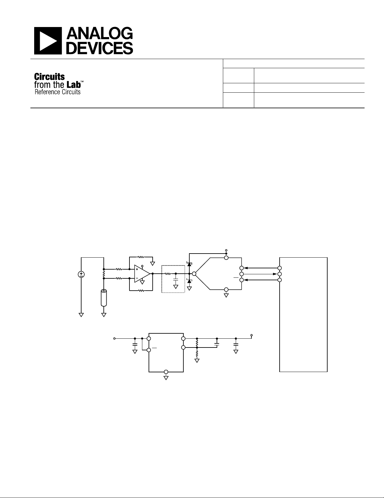
in Figure 1, uses the overvoltage protected ADA4096-2 op amp
connected as a difference amplifier to monitor the high-side
current. The ADA4096-2 has input overvoltage protection,
without phase reversal or latch-up, for voltages of 32 V higher
than and lower than the supply rails.
The circuit is powered by the ADP3336 adjustable low dropout
500 mA linear regulator, which can also be used to supply power to
other parts of the system, if desired. Its input voltage can range
from 5.2 V to 12 V when set for a 5 V output. To save power,
the current sensing circuit can be powered down by removing
power to the ADP3336; however, the power source, such as a
solar panel, can still operate.
30 V, Micropower, Overvoltage Protection,
Rail-to-Rail Input/Output Amplifier
High Accuracy Ultralow IQ 500 mA anyCAP®
Adjustable Low Dropout Linear Regulator
Circuits from the Lab™ circui
each circuit, and their function and performance have been tested and verified in a lab environment at
be liable for direct, indirect, special, incidental, consequential or punitive damages due to any cause
Figure 1. High-Side Current Sensing with Input Overvoltage Protection (Simplified Schematic: All Connections and Decoupling Not Shown)
One Technology Way, P.O. Box 9106, Norwood, MA 02062-9106, U.S.A.
Tel: 781.329.4700
www.analog.com

CN-0241 Circuit Note
R6
V
CC
+IN
–IN
V
EE
OVP
OVP
OUT
R7
D10 Q20
Q19
D11
Q16
D7Q15
D8
Q14
Q17
Q10
Q13
Q18D9
×1
I3
R2
R1
R3
R4
C2
Q12
D6
R5
Q9
Q11
Q6
Q8Q7
Q5
Q4
Q3
Q1 Q2
I2
I1
C1
D3
D1
D4
D2
10155-002
7
–48 –40 –32 –24 –16 –8 0 8 16 24 32 40 48
–7
–6
–5
–4
–3
–2
–1
0
1
2
3
4
5
6
INPUT BIAS CURRE NT (mA)
VIN (V)
V
EE
= –15V
V
EE
= 0V
V
CC
= +15V
LOW RDS
ON
SERIES FET
5kΩ SERIES RESISTOR
10155-003
This applies voltage to the inputs of the unpowered ADA4096-2;
however, no latch-up or damage occurs for input voltages up to
32 V. If slower throughput rates are required, the AD7920 can
also be powered down between samples. The AD7920 draws a
maximum of 5 µW when powered down and 15 mW when
powered up. The ADA4096-2 requires only 120 µA under
operational conditions. When operating at 5 V, this is only
0.6 m W. Th e ADP3336 draws only 1 µA in the shutdown mode.
CIRCUIT DESCRIPTION
The circuit is a classic high-side current sensing circuit topology
with a single sense resistor. The other four resistors (dual 1 kΩ/
20 kΩ divider) are in a thin film network (for ratio matching)
and are used to set the difference amplifier gain. This amplifies
the difference between the two voltages seen across the sense
resistor and rejects the common-mode voltage.
V
= (VA − VB) (20 kΩ/1 kΩ)
OUT
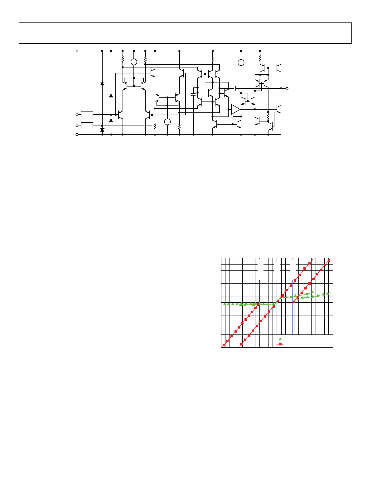
Figure 2 shows a simplified schematic of the ADA4096-2. The
input stage comprises two differential pairs (Q1 to Q4 and Q5 to
Q8) operating in parallel. When the input common-mode voltage
approaches V
minimum voltage compliance. Conversely, when the input
common-mode voltage approaches V
down as I2 reaches its minimum voltage compliance. This topology
allows for maximum input dynamic range because the amplifier
can function with its inputs at 200 mV outside the rail (at room
temperature).
As with any rail-to-rail input amplifier, V
the two input pairs determines the CMRR of the amplifier. If the
input common-mode voltage range is within 1.5 V of each rail,
transitions between the input pairs are avoided, thus improving
the CMRR by approximately 10 dB.
The ADA4096-2 inputs are protected from input voltage excursions
up to 32 V outside each rail. This feature is of particular importance
in applications with power supply sequencing issues that can cause
the signal source to be active before the supplies to the amplifier
are applied.
− 1.5 V, Q1 to Q4 shut down as I1 reaches its
CC
+ 1.5 V, Q5 to Q8 shut
EE
mismatch between
OS
Figure 2. ADA4096-2 Simplfied Schemactic
Figure 3 shows the input current limiting capability of the
ADA4096-2 provided by low RDS
curves) compared to using a 5 kΩ external series resistor with
an unprotected op amp (red curves).
Figure 3 was generated with the ADA4096-2 in a unity-gain
buffer configuration with the supplies connected to GND (or
±15 V) and the positive input swept until it exceeds the supplies
by 32 V. In general, input current is limited to 1 mA during positive
overvoltage conditions and 200 μA during negative undervoltage
conditions. For example, at an overvoltage of 20 V, the ADA4096-2
input current is limited to 1 mA, providing a current limit
equivalent to a series 20 kΩ resistor.
Figure 3 also shows that the current limiting circuitry is active
whether the amplifier is powered or not.
Figure 3 represents input protection under abnormal conditions
only. The correct amplifier operation input voltage range (IVR)
is specified in Table 2 to Table 4 of the ADA4096-2 data sheet.
Rev. A | Page 2 of 6
The AD7920 is a 12-bit, high speed, low power, successive
approximation ADC. The part operates from a single 2.35 V to
5.25 V power supply and features throughput rates up to 250 kSPS.
The part contains a low noise, wide bandwidth track-and-hold
amplifier that can handle input frequencies in excess of 13 MHz.
ON
Figure 3. Input Current Limiting Capability
internal series FETs (green
 Loading...