ANALOG DEVICES CN-0233 Service Manual

Circuit Note
Circuits from the Lab™ circuits from Analog Devices have been designed and built by Analog Devices
. Standard engineering practices have been employed in the design and construction of
each circuit, and their function and performance have been tested and verified in a lab environment at
suitability and applicability for your use and application. Accordingly, in no event shall Analog Devices
be liable for direct, indirect, special, incidental, consequential or punitive damages due to any cause
T1: COILTRONICS KA4976- AL
1:5 TURNS RATI O
+5V
+5V
ISO ISO
15kΩ
0.1%
5ppm/°C
4nF
ISO
ISO
ISO
ISO
R2 90.9kΩ
0.1µF
R3
10.5kΩ
ISO
R1 24.9kΩ
–15V (AVSS)
+15V (AVDD)
R
OC
100kΩ
D1 TO D4: MBR0540
DV
CCAVDD
–V
SENSE
R
L
CURRENT
OUTPUT
VOLTAGE
OUTPUT
V
OUT
R
SET
C
COMP
AV
SS
LATCH
SCLK
SDIN
SDO
CLR GND CLR SEL
FAULT
REFIN
I
OUT
+V
SENSE
AVDD
ISO ISOISO
ISO ISO
ISO
V
IN
ADR445
AD5422
V
OUT
AVSS
V
FB
1.25V
ADuM3471
+
+
+
ISO
ISO
+
+5V
IN
47µF
1
2
3
4
5
6
7
8
9
10
20
19
18
17
16
15
14
13
12
11
47µF
10µF 0.1µF
10µF 0.1µF 10µF 0.1µF 0.1µF
10µF 0.1µF
47µF
0.1µF
47µH
47µH
L1
D11:5
T1
D2
D3
D4
X1
GND
1
VDD
1
X2
I/OA
I/OB
I/OC
I/OD
I/OA
I/OB
I/OC
I/OD
V
DDA
GND
1
GND
2
V
REG
GND
2
VDD
2
FB
OC
L2
10126-001
Circuits from the Lab™ reference circuits are engineered and
tested for quick and easy system integration to help solve today’s
analog, mixed-signal, and RF design challenges. For more
information and/or support, visit www.analog.com/CN0233.
16-Bit Isolated Industrial Voltage and Current Output DAC
with Isolated DC-to-DC Supplies
EVALUATION AND DESIGN SUPPORT
Design and Integration Files
Schematics, Layout Files, Bill of Materials
CIRCUIT FUNCTION AND BENEFITS
Industrial and instrumentation systems, as well as programmable logic controllers (PLCs) and distributed control systems
(DCS), must often control outputs, which can be both current
controlled (4 mA to 20 mA), and voltage controlled (up to
±10 V). Typically, such designs also need to be isolated from the
local system controller to protect against ground loops and also
CN-0233
Devices Connected/Referenced
ADuM3471
AD5422
ADR445 Precision 5.0 V Reference
to ensure robustness against external events. Traditional solutions
use discrete ICs for both power and digital isolation.
When multichannel isolation is needed, the cost and space
of providing discrete solutions becomes a big disadvantage.
Solutions based on opto-isolators typically have reasonable
output regulation but require additional external components,
thereby increasing board area. Power modules are often bulky
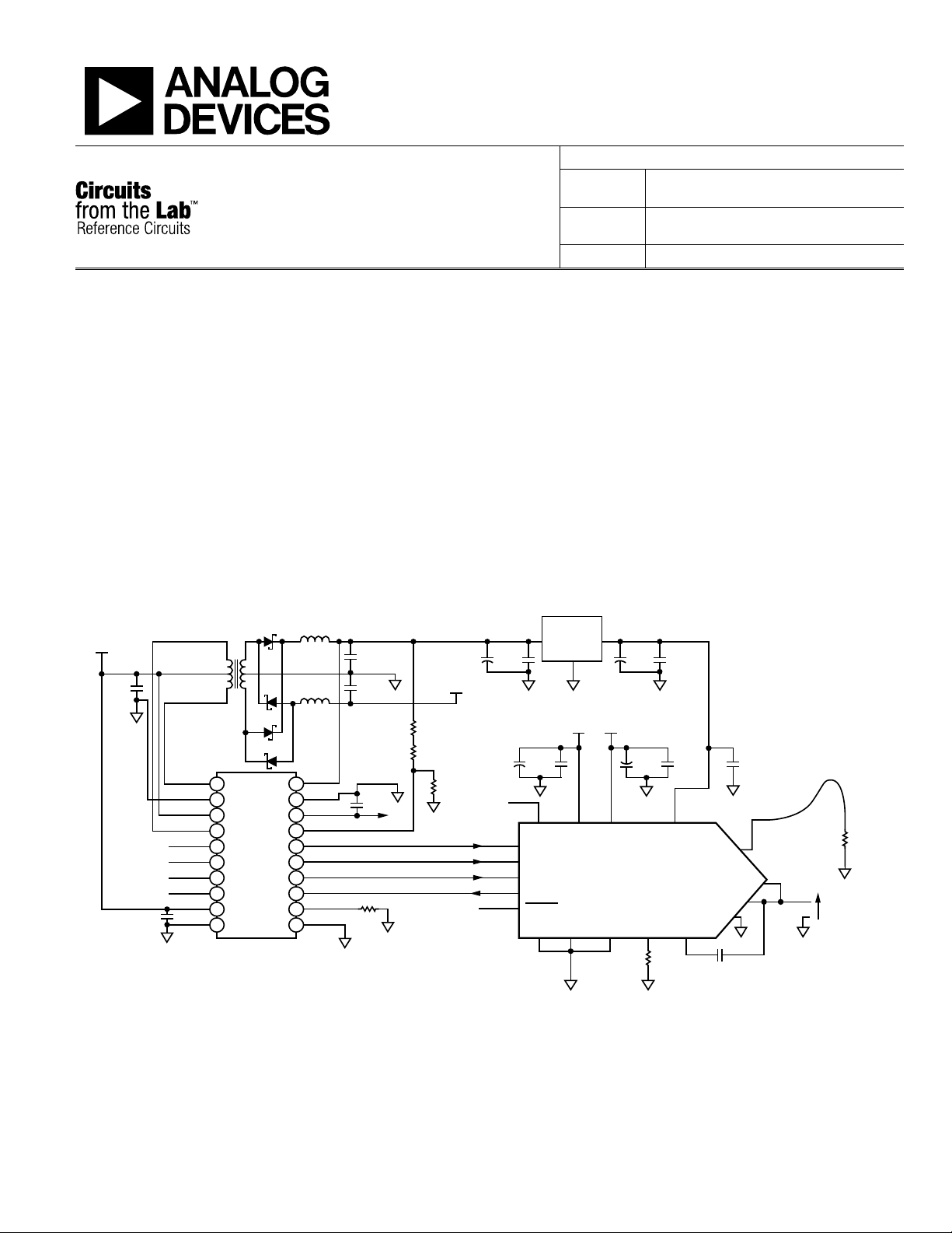
and may provide poor output regulation. The circuit in Figure 1
is based on the ADuM347x family of isolators (ADuM3470,
ADuM3471, ADuM3472, ADuM3473, ADuM3474) and
Quad Isolator with Integrated
Transformer Driver and PWM Controller.
16-Bit Current Source and Voltage
Output DAC
Rev.0
engineers
room temperature. However, you are solely responsible for testing the circuit and determining its
whatsoever connected to the use of any Circuits from the Lab circuits. (Continued on last page)
Figure 1. Isolated 16-Bit Current and Voltage Output DAC with Isolated Power Supplies.
One Technology Way, P.O. Box 9106, Norwood, MA 02062-9106, U.S.A.
Tel: 781.329.4700
Fax: 781.461.3113 ©2011
Analog Devices, Inc. All rights reserved.
www.analog.com

2.0
1.5
1.0
0.5
0
–0.5
–1.0
–1.5
–2.0
0 32,768 65,535
10126-002
INL (LS Bs)
CODE
2.0
1.5
1.0
0.5
0
–0.5
–1.0
–1.5
–2.0
0 32,768 65,535
10126-003
INL (LS Bs)
CODE
CN-0233 Circuit Note
integrates digital isolation, as well as the PWM-controlled
power regulation circuitry along with associated feedback
isolation. External transformers are used to transfer power
across the isolation barrier. The AD5422 16-bit DAC provides
the current and voltage outputs.
CIRCUIT DESCRIPTION
The AD5422 is a fully integrated, fully programmable 16-bit
voltage and current output DAC, capable of programming
ranges from 4 mA to 20 mA, 0 mA to 20 mA, 0 V to 5 V, 0 V to
10 V, ±5 V, ±10 V. The voltage output headroom is typically
1 V, and the current output needs about 2.5 V headroom.
This means that the 20 mA current output can drive a load of
approximately 600 Ω with a 15 V supply.
The ADuM347x devices are quad-channel digital isolators with
an integrated PWM controller and low impedance transformer
drivers (X1 and X2). The only additional components required
for an isolated dc-to-dc converter are a transformer and simple
full-wave diode rectifier. The devices provide up to 2 W of
regulated, isolated power when supplied from a 5.0 V or 3.3 V
input. This eliminates the need for a separate isolated dc-to-dc
converter.
The iCoupler chip-scale transformer technology is used to
isolate the logic signals, and the integrated transformer driver
with isolated secondary side control provides high efficiency
for the isolated dc-to-dc converter. The internal oscillator
frequency is adjustable from 200 kHz to 1 MHz and is
determined by the value of R
switching frequency is 500 kHz.
The ADuM3471 regulation is from the positive 15 V supply.
The feedback for regulation is from the divider network (R1,
R2, R3). The resistors are chosen such that the feedback voltage
is 1.25 V when the output voltage is 15 V. The feedback voltage
is compared with the ADuM3471 internal feedback setpoint
voltage of 1.25 V. Regulation is achieved by varying the duty
cycle of the PWM signals driving the external transformer.
The negative supply is loosely regulated and for light loads can
be as high as −23 V. This is within the maximum operating
value of −26.3 V. With nominal loads greater than 1 kΩ, the
additional power dissipation due to the larger unregulated
negative supply voltage is not a problem. In applications that
require higher compliance voltages or where very low power
dissipation is required, a different power supply design should
be considered.
This circuit was tested with the ADR445 5 V, high precision, low
drift (3 ppm/°C maximum for B grade) external reference. This
allows total system errors of less than 0.1% to be achieved over
the industrial temperature range (−40°C to +85°C).
. For ROC = 100 kΩ, the
OC
The AD5422 has a high precision integrated internal reference
with a drift of 10 ppm/°C maximum. If this reference is used
rather than the external reference, only 0.065% additional error
is incurred across the industrial temperature range.
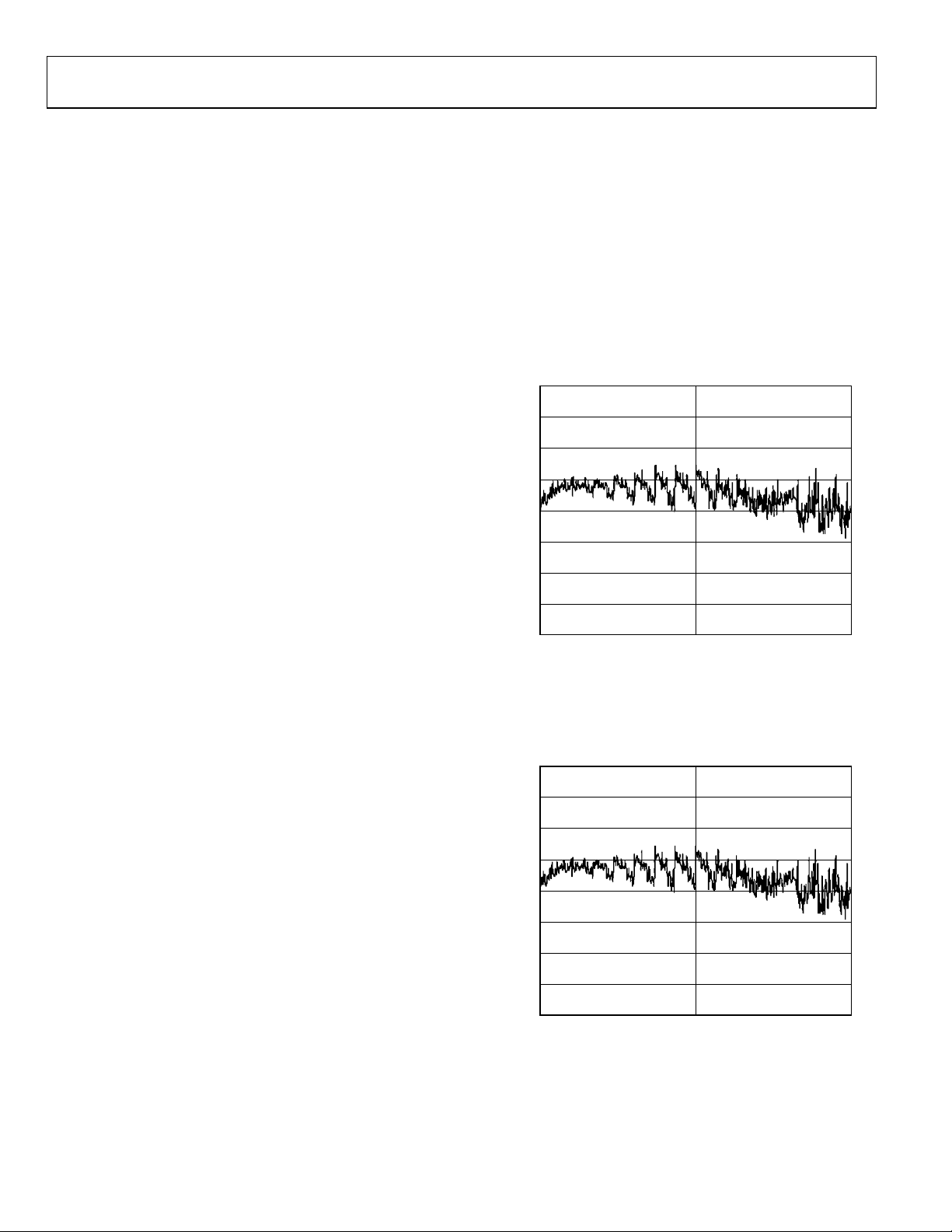
The AD5422 integral nonlinearity (INL) was tested using both
linear supplies and the isolated dc-to-dc switching supplies to
ensure no loss in system accuracy was incurred because of the
switching supplies. Figure 2 shows the INL for the linear
supplies and Figure 3 for the switching supplies. There is no
noticeable performance loss when using the switching supply as
compared to the linear supply.
Figure 2. Measured INL of Circuit for ±10V Output Range Using
Linear Supplies .
Figure 3. Measured INL of Circuit for ± 10V Output Range Using
Switching Supplies .
Rev. 0 | Page 2 of 4
 Loading...