Circuit Note
CN-0232
Fractional-N PLL Synthesizer with
Integrated VCO
Rev. 0
the Lab™ circuits from Analog Devices have been designed and built by Analog Devices
engineers. Standard engineering practices have been employed in the design and construction of
room temperature. However, you are solely responsible for testing the circuit and determining its
suitability and applicability for your use and application. Accordingly, in no event shall Analog Devices
irect, special, incidental, consequential or punitive damages due to any cause
whatsoever connected to the use of any Circuits from the Lab circuits. (Continued on last page)
Fax: 781.461.3113 ©2012 Analog Devices, Inc. All rights reserved.
22nF 4.7nF
100nF
360Ω
200Ω
ADF4153
CPGND DGND
CP
1nF1nF
4.7kΩ
R
SET
LE
DATA
CLK
REF
IN
DV
DD
MUXOUT
V
DD
SDV
DD
V
P
100pF
100pF
AV
DD
AGND
ADF4350
V
VCO
V
VCO
V
VCO
V
VCO
DV
DD
AV
DD
V
P
V
TUNE
CP
OUT
PDB
RF
SDV
DD
RF
OUT
B+
RF
OUT
B–
RF
OUT
A–
RF
OUT
A+
CE
V
DD
CPGND AGND DGND
4.7kΩ
R
SET
LE
DATA
CLK
REF
IN
MUXOUT
LOCK
DETECT
51Ω
A
GNDVCO
LD
SD
GND
TEMP V
REF
V
COM
SW
10pF 0.1µF
1nF
1nF
1nF
1nF
TCXO
26MHz
51Ω
51Ω
51Ω
51Ω
51Ω
51Ω 51Ω
RFOUTA+
VCO
COUNTERS
PHASE
FREQUENCY
DETECTOR
CHARGE
PUMP
COUNTERS
PHASE
FREQUENCY
DETECTOR
CHARGE
PUMP
RFOUTB+
VCO
TUNING
VOLTAGE
REFERENCE
LOOP FILTER
RF IN
3.3V
3.3V
3.3V
51Ω
10pF 0.1µF
10pF 0.1µF
1nF1nF
8
11
12
13
1
2
3
1
29
SPI COMPAT IBLE SERIAL BUS
RFINA
RF
IN
B
15
3
4
9
6
5
14
7
2
16 10
10
28
16
8 31 9 11 18 21 27
14
15
19 23 24
25
30
17
20
7
26
6 32
5
4
12
13
22
SPI COMPAT IBLE SERIAL BUS
10125-001
Circuits from the Lab™ reference circuits are engineered and
tested for quick and easy system integration to help solve today’s
analog, mixed-signal, and RF design challenges. For more
information and/or support, visit www.analog.com/CN0232.
Devices Connected/Referenced
ADF4350
ADF4153 Fractional-N PLL Frequency Synthesizer
Minimizing Spurious Outputs Using a Synthesizer with an Integrated VCO and
an External PLL Circuit
EVALUATION AND DESIGN SUPPORT
Circuit Evaluation Boards
ADF4350 Evaluation Board (EVAL-ADF4350EB2Z)
ADF4153 Evaluation Board (EVAL-ADF4153EBZ1)
Design and Integration Files
Schematics, Layout Files, Bill of Materials
CIRCUIT FUNCTION AND BENEFITS
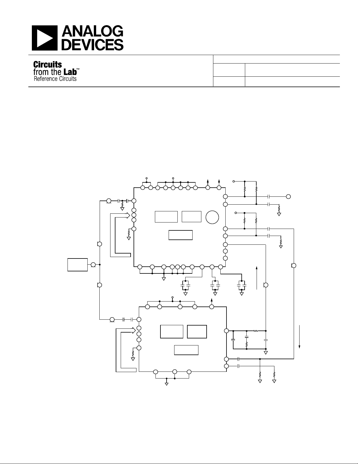
The circuit shown in Figure 1 uses the ADF4350 synthesizer with
an integrated VCO and an external PLL to minimize spurious
outputs by isolating the PLL synthesizer circuitry from the VCO
circuit.
Figure 1. ADF4153 PLL Connected to ADF4350 (Simplified Schematic: All Connections and Decoupling Not Shown)
Circuits from
each circuit, and their function and performance have been tested and verified in a lab environment at
be liable for direct, ind
One Technology Way, P.O. Box 9106, Norwood, MA 02062-9106, U.S.A.
Tel: 781.329.4700
www.analog.com

CN-0232 Circuit Note
Devices with integrated PLLs and VCOs may have feed through
from the digital PLL circuitry to the VCO, leading to higher
spurious levels due to the close proximity of the PLL circuitry
to the VCO.
The circuit shown in Figure 1 uses the ADF4350, a fully integrated
fractional-N PLL and VCO that can generate frequencies from
137.5 MHz to 4400 MHz, together with the ADF4153 PLL.
In addition to improvements in spurious performance,
another possible advantage of using an external PLL is the
possibility of increased frequency resolution. For example,
if the ADF4157 PLL is selected in place of the ADF4153, the
frequency resolution of the PLL can be as fine as 0.7 Hz.
CIRCUIT DESCRIPTION
The ADF4350 is a wideband PLL and VCO consisting of
three separate multiband VCOs. Each VCO covers a range of
approximately 700 MHz (with some overlap between the
frequencies of the VCO). This permits a fundamental VCO
frequency range of between 2.2 GHz to 4.4 GHz. Frequencies
lower than 2.2 GHz can be generated using internal dividers
within the ADF4350.
For most applications, the internal PLL of the ADF4350 is used to
lock the VCO. In addition to locking the PLL, the PLL circuitry
performs an additional vital function of VCO band select, using
the internal reference (R) and feedback (N) counters of the internal
PLL to compare the VCO output with the reference input.
For frequency generation, the internal PLL must be enabled and
the desired frequency must be programmed. Then, once sufficient
time has elapsed for band select, the internal PLL can be disabled,
and, finally, the external PLL can be enabled. The external PLL
compares the reference frequency and the VCO output frequency
to generate a stable dc voltage to lock the PLL.
Figure 2 shows the output frequency spurs measured at RF
OUT
A+
using the ADF4350 internal PLL and VCO with the ADF4153 PLL
disabled. Note the presence of PFD spurs at 13 MHz and 26 MHz.
Figure 3 shows the output spurs measured at RF
A+ with the
OUT
ADF4350 internal PLL circuit disabled and the external ADF4153
PLL active. In this mode, the charge pump output of the ADF4153
drives the loop filter, which in turn drives the V
ADF4350. The V
input controls the ADF4350 VCO output
TUNE
input of the
TUNE
fre quency.
In making a comparison between Figure 2 and Figure 3, the spurs
due to the phase frequency detector (PFD) frequency, at 13 MHz
and 26 MHz, in Figure 2 have disappeared into the noise floor
in Figure 3.
COMMON VARIATIONS
Different PLLs can be selected. The fractional-N PLL in both the
ADF4350 and ADF4153 has a minimum frequency resolution
of PFD/4095. If finer resolution is required, the ADF4157
can be selected. The resolution of this PLL is PFD/2
providing an ultrafine resolution of <1 Hz.
For applications requiring simpler software programmability,
the ADF4150 PLL is software compatible with the ADF4350,
easing the software programming sequence.
25
, thereby
Rev. 0 | Page 2 of 6
 Loading...