ANALOG DEVICES CN-0227 Service Manual

Circuit Note
S
Circuits from the Lab™ reference circuits are engineered and
tested for quick and easy system integration to help solve today’s
analog, mixed-signal, and RF design challenges. For more
information and/or support, visit w ww.analog.com/CN0227.
Devices Connected/Referenced
AD9467
ADL5562
16-Bit, 250 MSPS Analog-to-Digital
Converter
3.3 GHz Ultralow Distortion RF/IF
Differential Amplifier
CN-0227
High Performance, 16-Bit, 250 MSPS Wideband Receiver with Antialiasing Filter
EVALUATION AND DESIGN SUPPORT
Design and Integration Files
Schematics, Layout Files, Bill of Materials
CIRCUIT FUNCTION AND BENEFITS
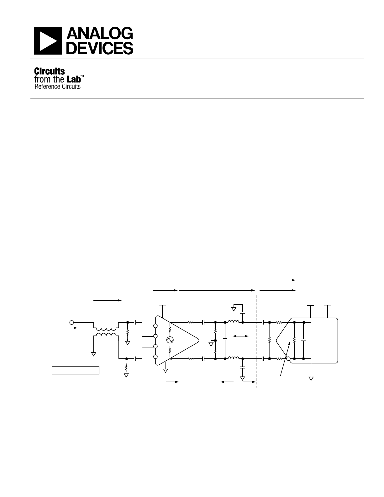
The circuit, shown in Figure 1, is a wideband receiver front end
based on the ADL5562 ultralow noise differential amplifier driver
and the AD9467 16-bit, 250 MSPS analog-to-digital converter.
The third-order Butterworth antialiasing filter is optimized based
on the performance and interface requirements of the amplifier
and ADC. The total insertion loss due to the filter network and
other components is only 1.8 dB.
The overall circuit has a bandwidth of 152 MHz with a pass band
flatness of 1 dB. The SNR and SFDR measured with a 120 MHz
analog input are 72.6 dBFS and 82.2 dBc, respectively.
5.7dB GAI N
+6.0dBm FS AT 10MHz
ANALOG INPUT
INPUT
Z = 50
OVERALL GAIN = 3.9dB
Figure 1. 16-Bit, 250 MSPS Wideband Receiver Front End (Simplified Schematic: All Connections and Decoupling Not Shown)
0.1dB LOSS
XFMR
1:1 Z
ECT1-1-13M
0.1µF
33
Z
= 400
I
0.1µF
33
Gains, Losses, and Signal Levels Measured Values at 10 MHz
+5V
VIP2
VIP1
VIN1
VIN2
6
ADL5562
G = 6dB
6
15
15
CIRCUIT DESCRIPTION
The circuit accepts a single-ended input and converts it to
differential using a wide bandwidth (3 GHz) M/A-COM
ECT1-1-13M 1:1 transformer. The ADL5562 3.3 GHz differential
amplifier has a differential input impedance of 400 Ω when
operating at a gain of 6 dB and 200 Ω when operating at a gain
of 12 dB. A gain option of 15.5 dB is also available.
The ADL5562 is an ideal driver for the AD9467, and the fully
differential architecture through the low-pass filter and into the
ADC provides good high frequency common-mode rejection,
as well as minimizes second-order distortion products. The
ADL5562 provides a gain of 6 dB or 12 dB depending on the input
connection. In the circuit, a gain of 6 dB was used to compensate
for the insertion loss of the filter network and transformer
(approximately 1.8 dB), providing an overall signal gain of 3.9 dB.
1.7dB LOS
1.2dB LO SS 0.5dB LO SS
+1.8V
+3.3V
62pF
0.1µF
0.1µF
243
243
22nH
FILTER
12pF
22nH
26938.6203
62pF
0.1µF
20
511
0.1µF
20
FS = 2V p-p DIFF
530
3.5pF
INTERNAL
INPUT Z
AD9467
16-BIT
250MSPS
ADC
10071-001
Rev. A
Circuits from the Lab™ circuits from Analog Devices have been designed and built by Analog Devices
engineers. Standard engineering practices have been employed in the design and construction of
each circuit, and their function and performance have been tested and verified in a lab environment at
room temperature. However, you are solely responsible for testing the circuit and determining its
suitability and applicability for your use and application. Accordingly, in no event shall Analog Devices
be liable for direct, indirect, special, incidental, consequential or punitive damages due to any cause
whatsoever connected to the use of any Circuits from the Lab circuits. (Continued on last page)
One Technology Way, P.O. Box 9106, Norwood, MA 02062-9106, U.S.A.
Tel: 781.329.4700 www.analog.com
Fax: 781.461.3113 ©2011–2012 Analog Devices, Inc. All rights reserved.

CN-0227 Circuit Note
H
An input signal of 6.0 dBm produces a full-scale 2 V p-p
differential signal at the ADC input.
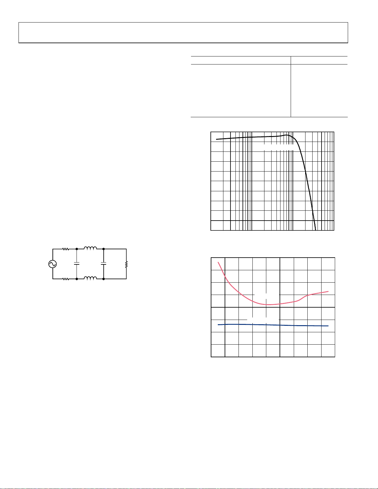
The antialiasing filter is a third-order Butterworth filter designed
with a standard filter design program. A Butterworth filter was
chosen because of its flat response within the pass band. A third
order filter yields an ac noise bandwidth ratio of 1.05 and can be
designed with the aid of several free filter programs such as
Nuhertz Technologies Filter Free, or the Quite Universal Circuit
Simulator (Qucs) Free Simulation.
To achieve best performance, load the ADL5562 with a net
differential load of 200 Ω. The 15 Ω series resistors isolate the
filter capacitance from the amplifier output, and the 243 Ω resistors
in parallel with the downstream impedance yield a net load
impedance of 203 Ω when added to the 30 Ω series resistance.
The 20 Ω resistors in series with the ADC inputs isolate internal
switching transients from the filter and the amplifier. The 511 Ω
resistor in parallel with the ADC serves to reduce the input
impedance of the ADC for more predictable performance.
The third-order Butterworth filter was designed with a source
impedance of 38.6 Ω, a load impedance of 269 Ω, and a 3 dB
bandwidth of 180 MHz. The calculated values from the program
are shown in Figure 1. The values chosen for the filter passive
components were the closest standard values to those generated
by the program.
19.3
23.83n
12pF 35.79pF
269
Table 1. Measured Performance of the Circuit
Performance Specs at 2 V p-p FS Final Results
Cutoff Frequency (−3 dB) 152 MHz
Pass-Band Flatness (6 MHz to 125 MHz) 1 dB
SNRFS at 120 MHz 72.6 dBFS
SFDR at 120 MHz 82.2 dBc
H2/H3 at 120 MHz 86.6 dBc/82.2 dBc
Overall Gain at 10 MHz 3.9 dB
Input Drive at 10 MHz 6.0 dBm
0
–2
–4
–6
–8
–10
–12
AMPLITUDE (dBFS)
–14
–16
–18
–20
1 10 100 1000
ANALOG INPUT FREQUENCY (MHz)
Figure 3. Pass Band Flatness Performance vs. Frequency
100
95
3dB AT 152MHz
10071-003
19.3
Figure 2. Design for Third-Order Differential Butterworth Filter with
Z
23.83nH
= 38.6 Ω, ZL = 269 Ω, FC = 180 MHz
S
10071-002
The internal 3.5 pF capacitance of the ADC was subtracted
from the value of the second shunt capacitor to yield a value of
32.29 pF. In the circuit, this capacitor was realized using two
62 pF capacitors connected to ground as shown in Figure 1.
This provides the same filtering effect and offers some ac
common-mode rejection.
The measured performance of the system is summarized in
Table 1, where the 3 dB bandwidth is 152 MHz. The total insertion
loss of the network is approximately 2 dB. The bandwidth response
is shown in Figure 3; the SNR and SFDR performance are
shown in Figure 4.
90
85
80
75
70
SNRFS (dBFS), SF DR (dBc)
65
60
0 20 40 60 80 100 120 140 160 180
Figure 4. SNR/SFDR Performance vs. Frequency
SFDR (dBc)
SNRFS (dBFS)
ANALOG INPUT FREQUENCY (MHz)
10071-004
Rev. A | Page 2 of 5
 Loading...