Circuit Note
engineers. Standard engineering practices have been employed in the design and construction of
each circuit, and their function and performance have been tested and verified in a lab environment at
suitability and applicability for your use and application. Accordingly, in no event shall Analog Devices
be liable for direct, indirect, special, incidental, consequential or punitive damages due to any cause
RBIP
50Ω
RBIN
50Ω
67
66
IBBN
IBBP
AD9122
ADL5375-05
RBQN
50Ω
RBQP
50Ω
59
58
21
22
9
10
RSLI
100Ω
RSLQ
100Ω
IOUT1N
IOUT1P
IOUT2P
IOUT2N
QBBP
QBBN
09740-001
LOW-PASS
FILTER
LOW-PASS
FILTER
Circuits from the Lab™ reference circuits are engineered and
tested for quick and easy system integration to help solve today’s
analog, mixed-signal, and RF design challenges. For more
information and/or support, visit www.analog.com/CN0205.
Interfacing the ADL5375 I/Q Modulator to the
AD9122 Dual Channel, 1.2 GSPS High Speed DAC
EVALUATION AND DESIGN SUPPORT
Circuit Evaluation Boards
AD9122/ADL5375 Evaluation Board (AD9122-M5375-EBZ)
Design and Integration Files
Schematics, Layout Files, Bill of Materials
CIRCUIT FUNCTION AND BENEFITS
This circuit provides a simple and flexible interface between
the AD9122 dual high speed TxDAC digital-to-analog
converter and the ADL5375-05 broadband I/Q modulator.
Because the DAC outputs and ADL5375-05 I/Q modulator
inputs share a common bias level of 0.5 V, there is no need
for any active or passive level shifting circuitry. The dc coupled
interface facilitates I/Q modulator local oscillator (LO) leakage
compensation by the DAC.
CN-0205
Devices Connected/Referenced
AD9122
ADL5375 Broadband Quadrature Modulator
The 1.2 GSPS AD9122 DAC sampling rate and the wide
bandwidth of the ADL5375-05 modulator I and Q inputs
ensure that both zero-IF (ZIF) or complex-IF (CIF)
architectures can be supported. In addition to filtering Nyquist
images, the baseband filter provides excellent rejection of both
differential-mode and common-mode DAC spurs.
CIRCUIT DESCRIPTION
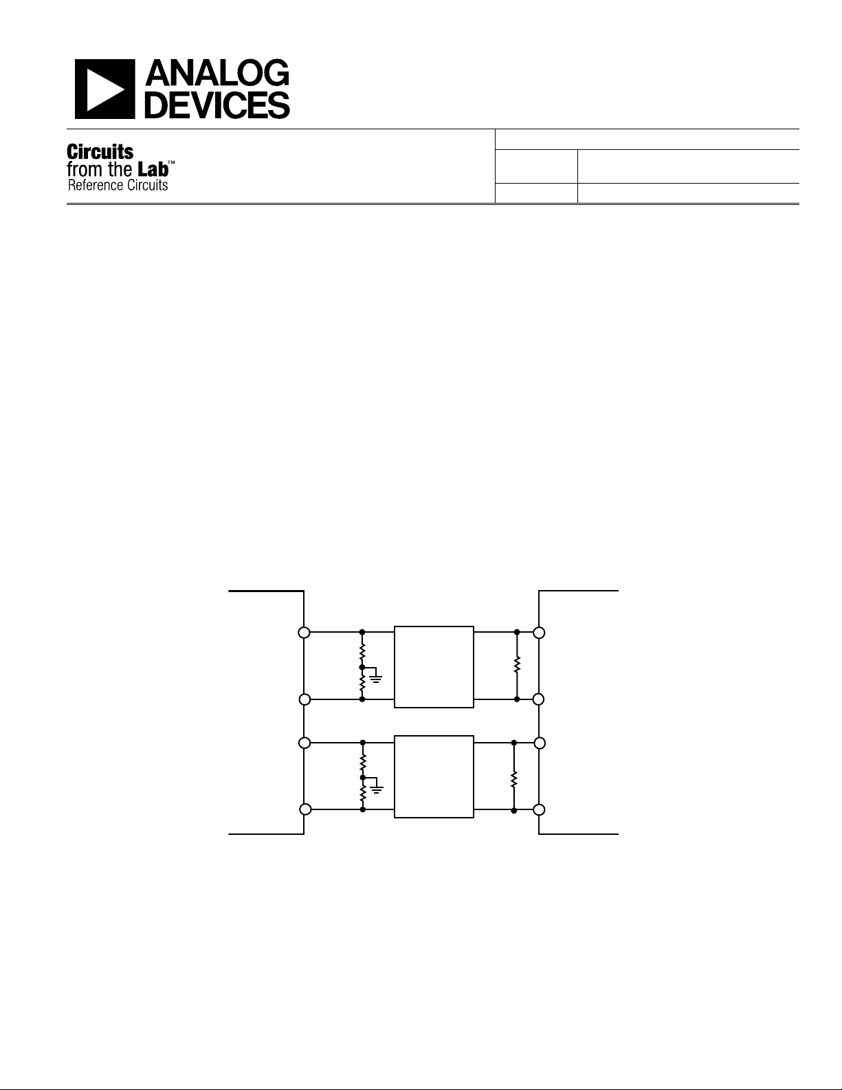
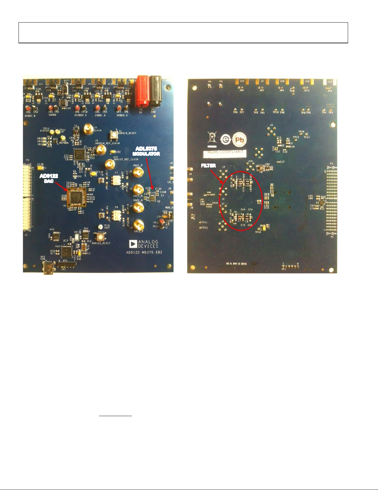
The circuit and board shown in Figure 1 and Figure2 utilize the
AD9122 TxDAC and the ADL5375-05 wideband transmit
modu lator. Signal biasing and scaling in the interface circuit is
controlled by the four ground-referenced resistors (RBIP, RBIN,
RBQP, RBQN) and the two shunt resistors (RSLI,RSLQ),
respectively.
Dual Channel, 1.2 GSPS, 16-Bit, TxDAC®
Digital-to Analog Conver ter
Rev. 0
Circuits from the Lab™ circuits from Analog Devices have been designed and built by Analog Devices
room temperature. However, you are solely responsible for testing th e circuit and determi ning its
whatsoever connected to the use of any Circuits from the Lab circuits. (Continued on last page)
Figure 1. Interface Between the AD9122 and ADL5375-05 with 50 Ω Resistors to Ground to Establish the
500 mV DC Bias for the ADL5375-05 Baseband Inputs (Simplified Schematic)
One Technology Way, P.O. Box 9106, Norwood, MA 02062-9106, U.S.A.
Tel: 781.329.4700
Fax: 781.461.3113 ©2011 Analog Devices, Inc. All rights reserved.
www.analog.com

CN-0205 Circuit Note
TOP VIEW
AD9122
DAC
ADL5375
MODULATOR
BOTTOM VIEW
FILTER
09740-002
[ ]
[ ]
LB
LB
FSSIGNAL
RR
RR
IV
+×
××
×=
2
2
Figure 2. AD9122-M5375-EBZ Evaluation Board for Circuit Implementation
The DA C’s full-scale output current (I
) is programmable from
FS
10 mA to 30 mA. The nominal and default value is 20 mA. In
this configuration, the DAC outputs swing from 0 mA to 20 mA
across each of the four ground-referenced 50 Ω resistors (R
RBIP = RBIN = RBQP = RBQN). This establishes the 500 mV
dc bias level and a full-scale voltage swing of 2 V p-p differential
on each output pair (with no load). This 2 V p-p voltage swing
can be adjusted by the R
(RL = RSLI = RSLQ) shunt resistors
L
without affecting the 500 mV bias level. The resulting
differential peak-to-peak swing at the I/Q modulator input
is given by the equation
Note that the relatively high differential input impedance of the
ADL5375 (typically >60 kΩ) can be ignored when calculating
this signal level. Figure 3 shows the relationship between the
=
B
peak-to-peak voltage swing and R
when 50 Ω bias-setting
L
resistors are used.
The ADL5375-05 and AD9122 are well matched in terms of
dynamic range and gain. As a result, there is no need for any
active gain between the devices. The I/Q modulator drive level
can be fine tuned as needed by adjusting the value of R
L
as
described above. For most applications, a value of 100 Ω for
R
is recommended. This results in a full-scale signal level of
L
1 V p-p (DAC output at 0 dBFS).
Rev. 0 | Page 2 of 9

Circuit Note CN-0205
2.0
1.8
1.6
1.4
1.2
1.0
0.8
0.6
0.4
0.2
0
10 100 1k 10k
DIFFERENTIAL SWING (V p-p)
R
L
(Ω)
09740-003
RBIP
50Ω
RBIN
50Ω
67
66
21
22
IBBN
IBBP
AD9122 ADL5375-05
RBQN
50Ω
RBQP
50Ω
59
58
9
10
RSLI
100Ω
RSLQ
100Ω
OUT1_N
OUT1_P
OUT2_P
OUT2_N
QBBP
QBBN
LPI
771.1nH
LNI
771.1nH
53.62pF
C1I
350.1pF
C2I
LNQ
771.1nH
LPQ
771.1nH
53.62pF
C1Q
350.1pF
C2Q
09740-004
1 10 100
–60
–50
–40
–30
–20
–10
0
0
6
12
18
24
30
36
GROUP DEL AY ( ns)
FREQUENCY (MHz)
MAGNITUDE ( dB)
MAGNITUDE
GROUP DEL AY
09740-005
Figure 3. Peak-to-Peak Differential Swing and the Swing Limiting
Baseband Filtering
A filter must be inserted between the AD9122 and ADL5375 to
remove Nyquist images, spurs, and broadband noise originating
from the DAC. The filter should be placed between the dc bias
setting resistors and the ac swing-limiting resistor. With this
configuration, the dc bias setting resistors (R
the signal scaling resistors (R
source and load resistances for the filter design.
Figure 4 shows a third-order Bessel low-pass filter with a −3 dB
frequency of 10 MHz. Matching input and output impedances of
the filter makes the filter design easy and results in better
passband flatness, which allows wide bandwidth filter designs.
In this example, the shunt resistor chosen is 100 Ω, producing
an ac swing of 1 V p-p differential. The frequency response of
this filter is shown in Figure 5.
Figure 4. DAC Modulator Interface with 10 MHz Third-Order, Bessel Filter
Resistor (R
) with 50 Ω Bias-Setting Resistors
L
B
in Figure 4) conveniently set the
L
in Figure 4) and
Filtering for Complex IF (CIF) Applications
Figure 6 shows the frequency response of the ADL5375
baseband I and Q inputs. Because this device has a wide and flat
frequency response (−3 dB point = 750 MHz), it is well suited to
complex IF (CIF) applications where the output signal from the
DAC has been digitally upconverted. In CIF applications, a lowpass Nyquist filter is still desirable, primarily because the dc bias
level can be preserved from the DAC output to the modulator
input.
The filter topology shown in Figure 7 is a 5
filter with a 300 MHz corner frequency and is the
recommended filter topology. A purely differential filter can
reject differential-mode images, spurs, and noise from the DAC.
Using two capacitors with their common connection grounded
(C2 and C4 in Figure 7) diverts some of the common-mode
current to ground and results in better common-mode rejection
of high-frequency signals than would be obtained with a purely
differential filter.
The simulated and measured responses of this filter are shown
in Figure 8 and Figure 9. The measured flatness is ±0.6 dB from
dc to 250 MHz and ±0.4 dB from 125 MHz to 250 MHz. This
data was taken with the AD9122 inverse sinc function on. In
this configuration, Figure 10 shows the common-mode
rejection performance of the 2 × F
common-mode frequency with and without IF filter shown in
Figure 7.
Rev. 0 | Page 3 of 9
Figure 5. Frequency Response for DAC Modulator Interface with
10 MHz Third-Order Bessel Filter
th
order Butterworth
common-mode spur vs.
DAC
 Loading...