ANALOG DEVICES CN-0200 Service Manual

Circuit Note
Circuits from the Lab™ circuits from Analog Devices have been designed and built by Analog Devices
each circuit, and their function and performance have been tested and verified in a lab environment at
room temperature. However, you are solely responsible for testing the circuit and determining its
suitability and applicability for your use and application. Accordingly, in no event shall Analog Devices
be liable for direct, indirect, special, incidental, consequential or punitive damages due to any cause
+
+
+
+
+
968 3 2
15 17 16 19
20
24
1
CLR
IOV
CCVCCVDD
BUFFERED
V
REFP
V
REFP
V
SS
V
REFN
AGND
–10V TO +10V
OUTPUT
VOLTAGE
0V TO +10V
DGND
V
OUT
R
FB
7
LDAC
11
SDO
14
INV
13
SCLK
SYNC
AD5780
AD8675
AD8675
12
SDIN
4
RESET
+15V
+15V
+10V
–15V
–15V
10µF
C1
10µF
A1
A2
0.1µF
10µF
+3.3V +15V
+15V
–15V
0.1µF
10µF
0.1µF
10µF
0.1µF
0.1µF
R1
1.5kΩ
R3*
1kΩ
6.8kΩ
6.8kΩ
SPI INTERFACE
AND DIGITAL
COTNROL
R2*
1kΩ
ADR445
GND
V
INVOUT
09697-001
*FOR OPTIMUM PERFORMANCE OVER TEMPERATURE,
R2 AND R3 SHOULD BE IN A SINGLE PACKAGE.
Circuits from the Lab™ reference circuits are engineered and
tested for quick and easy system integration to help solve today’s
analog, mixed-signal, and RF design challenges. For more
information and/or support, visit www.analog.com/CN0200.
18-Bit, Linear, Low Noise, Precision Bipolar ±10 V DC Voltage Source
EVALUATION AND DESIGN SUPPORT
Circuit Evaluation Boards
AD5780 Circuit Evaluation Board (EVAL-AD5780SDZ)
System Demonstration Platform (EVAL-SDP-CB1Z)
Design and Integration Files
Schematics, Layout Files, Bill of Materials
CIRCUIT FUNCTION AND BENEFITS
The circuit shown in Figure 1 is an 18-bit linear, low noise,
precision bipolar (±10 V) voltage source with a minimum
CN-0200
Devices Connected/Referenced
AD5780 True 18-Bit, Voltage Output DAC
AD8675
AD8676
ADR445
amount of external components. The AD5780 DAC is an 18-bit,
unbuffered voltage output DAC operating from a bipolar supply
of up to 33 V. The AD5780 accepts a positive reference input
range of 5 V to VDD − 2.5 V, and a negative reference input
range of VSS + 2.5 V to 0 V. Both reference inputs are buffered
on the chip, and external buffers are not required. The AD5780
offers a relative accuracy specification of ±1 LSB maximum, and
operation is guaranteed monotonic, with a ±1 LSB maximum
DNL specification.
Ultraprecision, 36 V, 2.8 nV√Hz,
Rail-to-Rail Output Op Amp
Ultraprecision, 36 V, 2.8 nV√Hz, Dual
Rail-to-Rail Output Op Amp
Ultralow Noise 5V LDO XFET® Voltage
Reference
Rev.0
engineers. Standard engineering practices have been employed in the design and construction of
whatsoever connected to the use of any Circuits from the Lab circuits. (Continued on last page)
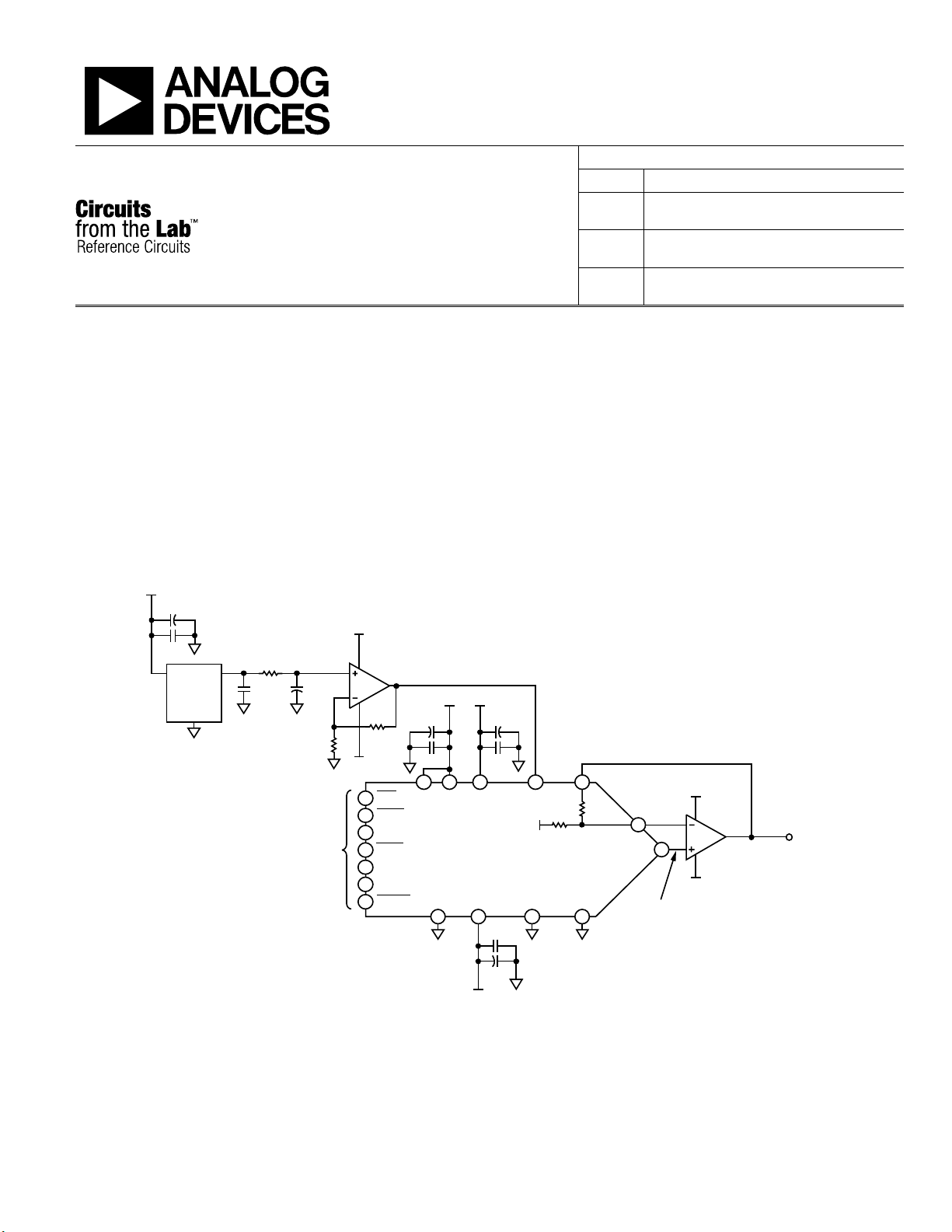
Figure 1. 18-Bit Accurate, +10 V Voltage Source (Simplified Schematic: All Connections and Decoupling Not Shown)
One Technology Way, P.O. Box 9106, Norwood, MA 02062-9106, U.S.A.
Tel: 781.329.4700
Fax: 781.461.3113 ©2011 Analog Devices, Inc. All rights reserved.
www.analog.com

CN-0200 Circuit Note
–0.4
–0.3
–0.2
–0.1
0
0.1
0.2
0.3
0.4
0.5
0.6
0 50000 100000 150000 200000 250000
INL (LSB)
DAC CODE
09697-002
–0.2
–0.1
0
0.1
0.2
0.3
0.4
0.5
0 50000 100000 150000 200000 250000
DNL (LSB)
DAC CODE
09697-003
The AD8675 precision op amp has low offset voltage (75 µV
maximum), low noise (2.8 nV/√Hz typical), and is an optimum
output buffer for the AD5780. The AD5780 has two internal
matched feedforward and feedback resistors, which are
connected to the AD8675 op amp and provide the 10 V offset
voltage. This allows an output voltage swing of ±10 V with a
single external 10 V reference.
The digital input to the circuit is serial and is compatible with
standard SPI, QSPI, MICROWIRE®, and DSP interface standards.
For high accuracy applications, the compact circuit offers high
precision, as well as low noise—this is ensured by the
combination of the AD5780, ADR445, and AD8675 precision
components.
This combination of parts provides industry-leading 18-bit
integral nonlinearity (INL) of ±1 LSB and differential
nonlinearity (DNL) of ±0.75 LSB, with guaranteed
monotonicity, as well as low power, small PCB area, and
cost effectiveness in an LFCSP package.
CIRCUIT DESCRIPTION
The digital-to-analog converter (DAC) shown in Figure 1 is the
AD5780, a high voltage, 18-bit converter with SPI interface,
offering ±1 LSB INL, ±0.75 LSB DNL, and 7.5 nV/√Hz noise
spectral density. The AD5780 also exhibits an extremely low
temperature drift of 0.005 LSB/°C.
Figure 1 shows the AD5780 configured in a gain-of-two mode
such that a single reference source can be used to generate a
symmetrical bipolar output voltage range. This mode of
operation uses an external op amp (A2), as well as on-chip
resistors (see AD5780 data sheet), to provide the gain of 2.
These internal resistors are thermally matched to each other
and to the DAC ladder resistance, resulting in ratiometric
thermal tracking. The output buffer is again the AD8675, used
for its low noise and low drift. This amplifier is also used (A1)
to amplify the +5 V reference voltage from the low noise
ADR445 to +10 V. R2 and R3 in this gain circuit are precision
metal foil resistors with 0.01% tolerance and a temperature
coefficient resistance of 0.6 ppm/°C. For optimum performance
over temperature, R1 and R2 should be in a single package, such
as the Vishay 300144 or VSR144 series. R2 and R3 are selected
to be 1 kΩ to keep noise in the system low. R1 and C1 form a
low-pass filter with a cutoff frequency of approximately 10 Hz.
The purpose of this filter is to attenuate voltage reference noise.
Linearity Measurements
The precision performance of the circuit shown in Figure 1 is
demonstrated on the EVAL -AD5780SDZ evaluation board
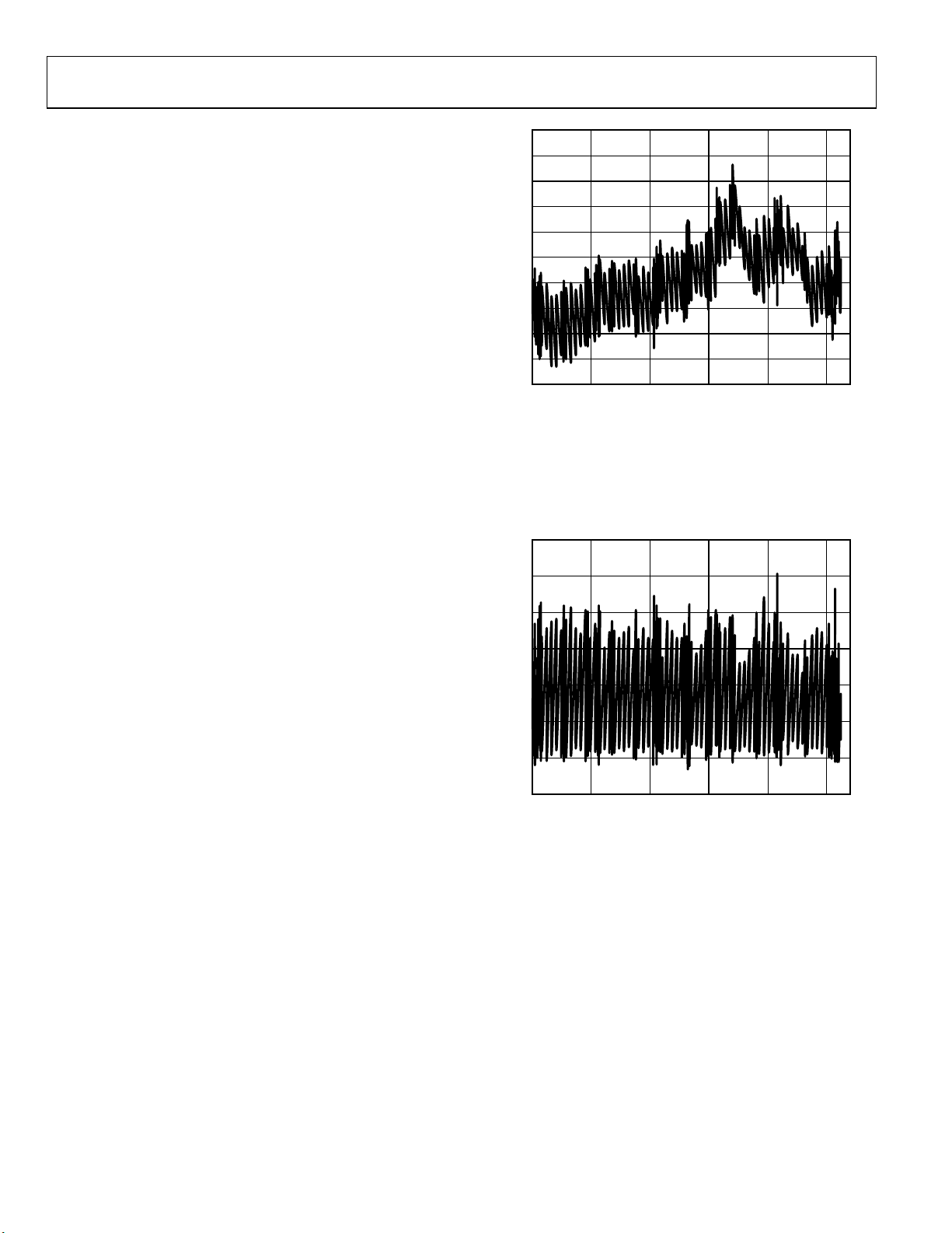
using an Agilent 3458A Multimeter. Figure 2 shows the integral
nonlinearity as a function of DAC code is within specifications
of ±1 LSB.
Figure 2. Integral Nonlinearity vs. DAC Code
Figure 3 shows that the differential nonlinearity as a function of
DAC code is within the −0.25 LSB to +0.75 LSB specification.
Figure 3. Differential Nonlinearity vs. DAC Code
Noise Drift Measurements
To be able to realize high precision, the peak-to-peak noise at
the circuit output must be maintained below 1 LSB, which is
76.29 µV for 18-bit resolution and a 20 V peak-to-peak voltage
range.
A real-time noise application will not have a high-pass cutoff at
0.1 Hz to attenuate 1/f noise but will include frequencies down
to dc in its pass band. With this in mind, the measured peak-topeak noise is realistically shown in Figure 4. In this case, the
noise at the output of the circuit was measured over a period of
100 seconds, effectively including frequencies as low as 0.01 Hz
in the measurement. The upper frequency cutoff is at approximately 14 Hz and is limited by the measurement setup.
Rev. 0 | Page 2 of 6
 Loading...