ANALOG DEVICES CN-0183 Service Manual

CN-0183
Rev. 0
engineers. Standard engineering practices have been employed in the design and construction of
each circuit, and their function and performance have been tested and verified in a lab environment at
temperature. However, you are solely responsible for testing the circuit and determining its
suitability and applicability for your use and application. Accordingly, in no event shall Analog Devices
equential or punitive damages due to any cause
whatsoever connected to the use of any Circuits from the Lab circuits. (Continued on last page)
Fax: 781.461.3113 ©2012 Analog Devices, Inc. All rights reserved.
+
+
+
+
DAC A
DAC H
V
OUT
A
V
OUT
H
V
REFIN/VREFOUT
GND
V
DD
SYNC
SCLK
DIN
LDAC
CLR
V
S
OUTPUT
GND
1.5kΩ
1.5kΩ
52.3kΩ
SW
100nF
VIN
EN
BST
ADP2300
GND
FB
10kΩ
10kΩ
V
IN
= +12V
+5V
+5V
–5V
+5V
10µF 0.1µF
10µF 0.1µF
1µF
TP2
+2.5V
0V TO +2. 5V
AD8638
L1
L1: COILCRAFT, L P D4012- 472M LB,
COUPLED I NDUCTOR, 4.7µ H
REF192
AD5668
TP1
DAC_OUT
BIPOLAR_OUT
−2.5V TO +2.5V
R2
10kΩ
R1
10kΩ
4.7µF
1µF
10µF
+
10µF
+5V
–5V
09471-001
Circuits from the Lab™ reference circuits are engineered and
tested for quick and easy system integration to help solve today’s
analog, mixed-signal, and RF design challenges. For more
information and/or support, visit www.analog.com/CN0183.
Precision 16-Bit, Bipolar Output Voltage Source with +12 V to ±5 V Supply
EVALUATION AND DESIGN SUPPORT
Circuit Evaluation Boards
CN-0183 Circuit Evaluation Board (EVAL-CN0183-SDZ)
System Demonstration Platform (EVAL-SDP-CB1Z)
Design and Integration Files
Schematics, Layout Files, Bill of Materials
CIRCUIT FUNCTION AND BENEFITS
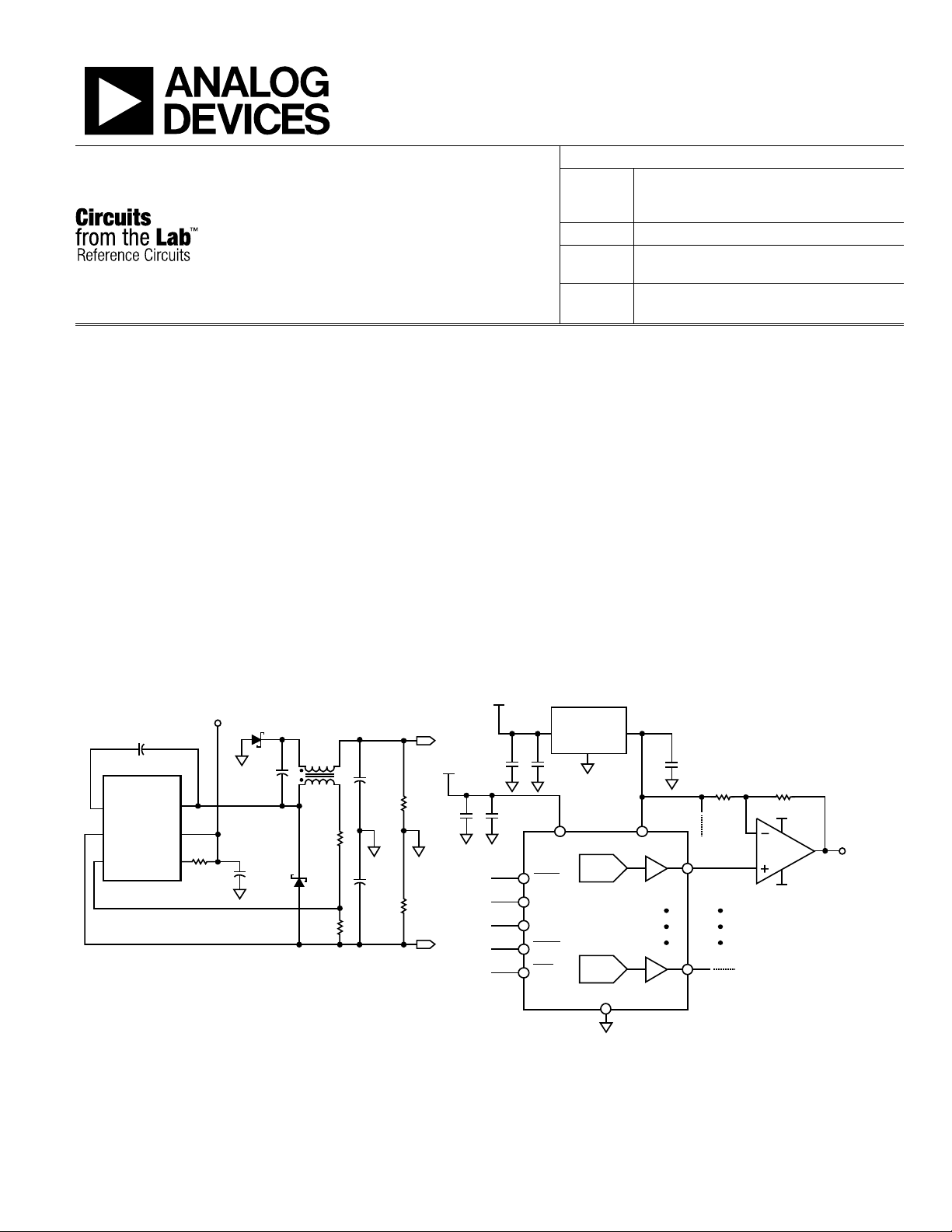
The circuit shown in Figure 1 provides a precision 16-bit, low
drift bipolar voltage output of ±2.5 V and operates on a single
+10 V to +15 V supply. The unipolar voltage outputs of the
AD5668 octal denseDAC are amplified and level shifted by the
AD8638 auto-zero op amps. The maximum drift contribution
Circuit Note
Devices Connected/Referenced
16-Bit Voltage Output denseDAC with
AD5668
AD8638 16 V Auto-Zero, Rail-to-Rail Output Op Amp
ADP2300
REF192
of the AD8638 is only 0.06 ppm/°C. The external REF192 reference
ensures a maximum drift of 5 ppm/°C (E grade) and provides a
low impedance pseudo ground for the AD8638 level gain and
shifting circuit.
The circuit offers an efficient solution to a problem often
encountered in systems with a single +12 V supply rail. Proper
printed circuit board (PCB) layout and grounding techniques
ensure that the ADP2300 switching regulator does not degrade
the overall performance of the circuit.
5 ppm/°C On-Chip Reference and SPI
Interface
1.2 A, 20 V, 700 kHz, Nonsynchronous StepDown Switching Regulator
Precision Micropower, 2.5 V Low Dropout
Voltage Reference
Circuits from the Lab™ circuits from Analog Devices have been designed and built by Analog Devices
room
be liable for direct, indirect, special, incidental, cons
Figure 1. Bipolar Output DAC Circuit with ±5 V Power Supplies
One Technology Way, P.O. Box 9106, Norwood, MA 02062-9106, U.S.A.
Tel: 781.329.4700
www.analog.com

CN-0183 Circuit Note
6
5
4
3
2
1
0
INL (LSB)
–1
–2
–3
–4
–5
0 10000 20000 30000
DAC CODE
40000 50000 60000
09471-002
0.6
0.4
0.2
0
DNL (LSB)
–0.2
–0.4
–0.8
–0.6
0 10000 20000 30000
DAC CODE
40000 50000 60000
09471-003
8
6
4
2
INL (LSB)
0
–2
–6
–4
0 10000 20000 30000
DAC CODE
40000 50000 60000
09471-004
0.8
0.6
0.4
0.2
0
–0.2
–0.4
DNL (LSB)
–0.6
–0.8
–1.0
0 10000 20000 30000
DAC CODE
40000 50000 60000
09471-005
CIRCUIT DESCRIPTION
The AD5668 is a 16-bit, octal, voltage output denseDAC
controlled by an SPI interface. It contains an on-chip reference
with a 10 ppm/°C maximum drift specification. The on-chip
reference is off at power-up, allowing the use of an external
reference. The internal reference is enabled via a software write.
In the circuit shown in Figure 1, an external REF192 is used
because a low output impedance is required to drive the 2.5 V
pseudo ground reference for the AD8638 op amps.
The output voltage of the AD5668 is 0 V to 2.5 V at TP1, and
this signal drives the noninverting input of the AD8638 op amp.
The signal gain of the op amp is 1 + R2/R1, which is 2 for R1 = R2.
A negative 2.5 V offset is injected into the op amp output by
driving R1 with the 2.5 V reference. The result is a bipolar
output voltage at TP2 that swings from −2.5 V to +2.5 V.
The circuit operates on a single supply voltage of nominally 12 V,
which can vary between 10 V and 15 V. The regulated −5 V
supply rail is developed from an ADP2300 switching regulator
connected in the inverting buck-boost configuration. The circuit
can be designed using the ADIsimPower program available at
www.analog.com/ADIsimPower. The L1 coupled inductor is
used to develop an unregulated 5 V supply for the circuit using
a Zeta configuration. This circuit yields high efficiency for small
output currents.
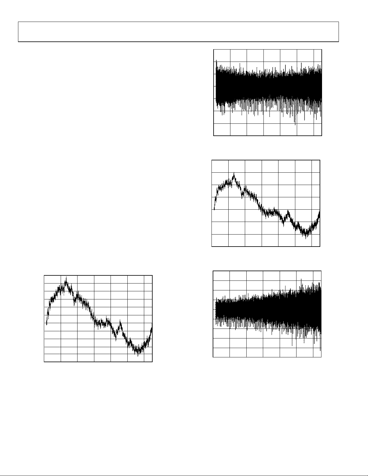
The integral nonlinearity (INL) and differential nonlinearity
(DNL) measured at TP2 (bipolar output) are shown in Figure 2
and Figure 3, respectively.
The INL and DNL measured at TP1 (unipolar DAC output) are
shown in Figure 4 and Figure 5, respectively.
Figure 3. DNL Performance of Bipolar Output (TP2)
Figure 4. INL Performance of Unipolar DAC Output (TP1)
Figure 2. INL Performance of Bipolar Output (TP2)
Rev. 0 | Page 2 of 5
Figure 5. DNL Performance of Unipolar DAC Output (TP1)
 Loading...