

Page 1
AN-260
a
APPLICATION NOTE
One Technology Way • P.O. Box 9106 • Norwood, MA 02062-9106 • 781/329-4700 • World Wide Web Site: http://www.analog.com
Using Digitally Programmable Delay Generators
by Allen Hill, IED
The AD9500 and AD9501 digitally programmable delay
generators are versatile parts, useful in numerous applications. The parts are designed for use in automatic test
equipment as a deskew element for digital data lines.
The versatility of the AD9500 and AD9501 for generating
programmable delays allows them to be used in applications that range from ATE to communications, computers, disk drives, lasers and ultrasound systems. This
note describes how best to apply these parts in some of
these applications.
GENERAL DESCRIPTION
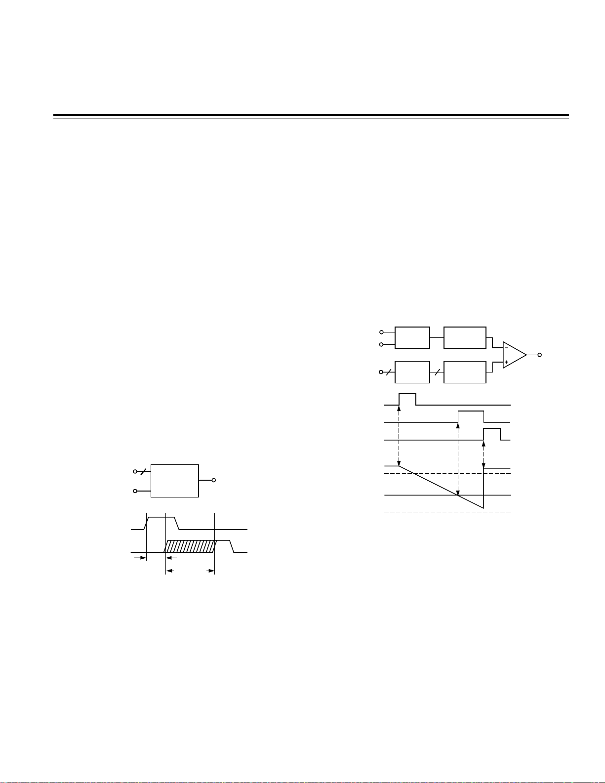
A digitally programmable delay generator delays a digital edge by a programmed amount of time. Figure 1
shows the basic function of a programmable delay generator. The delay through the device is controlled by an
N-bit digital word. This is the programmed delay. A trigger pulse is applied to the input, and after a fixed propagation delay (t
), the pulse edge appears a program
PD
delay later at the output.
comparator threshold set by the DAC, the output of the
comparator switches.
This output is delayed from the trigger pulse by an
amount of time that is proportional to the DAC digital
input code and the slope of the ramp. Altering the digital
delay value changes the DAC output voltage, which alters the delay through the circuit. The slope of the ramp
is controlled with external components.
TRIGGER
RESET
DIGITAL
DELAY
VALUE
TRIGGER
DELAYED
OUTPUT
RESET
TIMING
CONTROL
FLIP-FLOP
N N
LATCH
RAMP
GENERATOR
D/A
CONVERTER
DELAYED
OUTPUT
COMPARATOR
DIGITAL
DELAY
VALUE
TRIGGER
TRIGGER
PULSE
OUTPUT
PULSE
N
GENERATOR
t
PD
DELAY
PROGRAM
OUTPUT
DELAY
Figure 1. Programmable Delay Generator
The AD9500 (ECL) and AD9501 (TTL) use a ramp/comparator/DAC architecture as shown in Figure 2. One
input of a high speed comparator is driven by a digitalto-analog converter (DAC). The DAC is used to set a reference voltage at this comparator input. The other input
is connected to a ramp generator. The ramp generator is
started by applying a pulse to the trigger input of the
delay generator. When the ramp voltage crosses the
RAMP
VOLTAGE
DAC
VOLTAGE
(DAC CODE
00 HEX)
(DAC CODE
FF HEX)
Figure 2. Delay Generator Block Diagram and Basic
Timing
Once the comparator has switched, the ramp generator
and comparator must be reset so that the device can be
triggered again. One method of accomplishing the reset
is to connect the output of the delay generator to the
reset pin. This results in an output pulsewidth that is
equal to the reset propagation delay of the device (7 ns
to 15 ns). An alternate, and versatile, method of resetting the device is to use an external signal that meets the
timing requirements of the part. An external reset signal
allows the pulsewidth to be controlled and makes system integration of the delay signal easier.
Page 2
AN-260
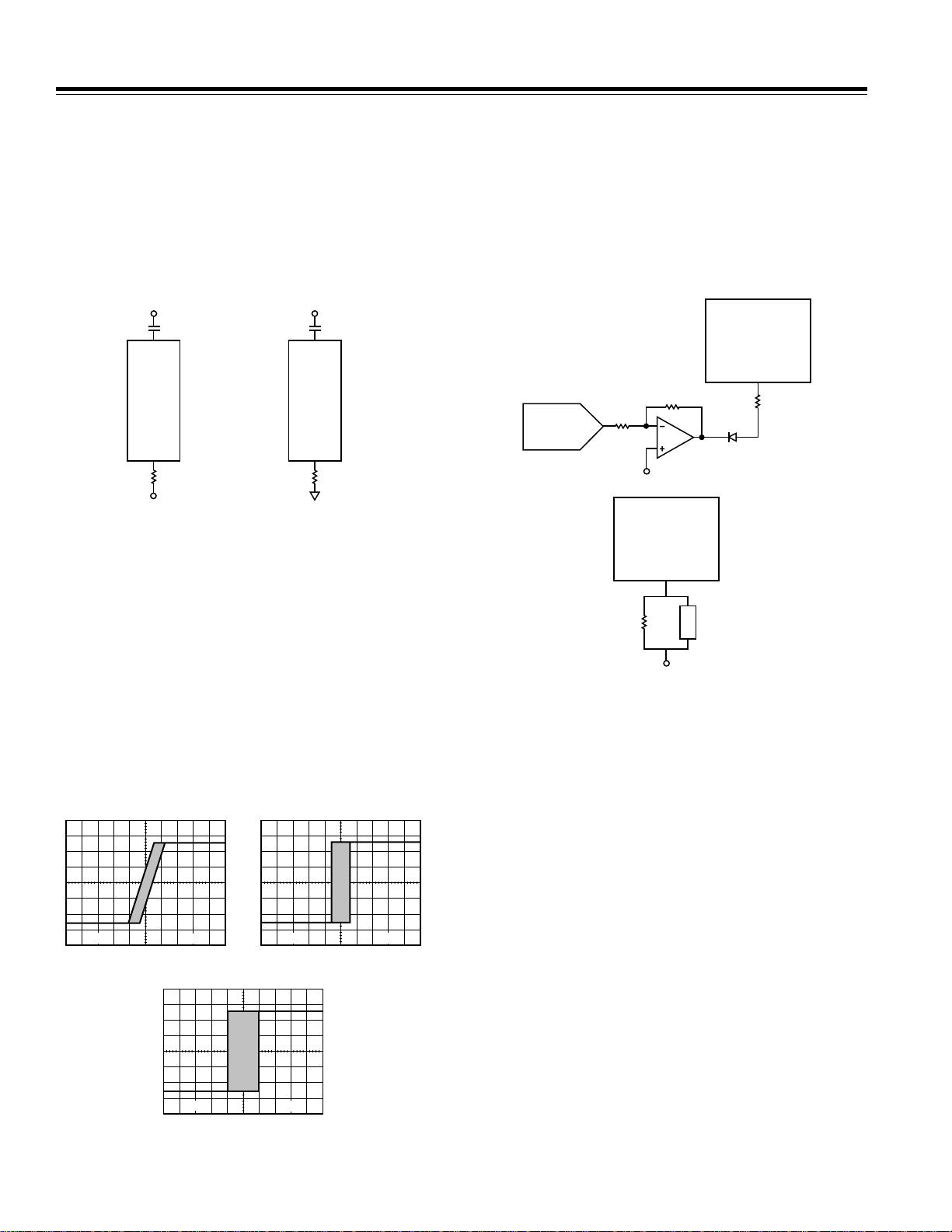
Full-Scale Range Setting
The full-scale range of the generator is the span over
which the delay can be programmed. This range is divided into 256 equal delays by the 8-bit digital delay
value. The full-scale range of the delay generator is configured by connecting R
SET
and C
as shown in Figure
EXT
3. Additional information is available on the AD9500 and
AD9501 data sheets. The range can be adjusted from a
minimum of 2.5 ns out to 10 µs and beyond.
+5V
C
EXT
7
AD9500
18
R
SET
–5.2V
FULL-SCALE RANGE =
3 (C
EXT
+10pF)
R
SET
3.84 3 R
+5V
C
EXT
6
AD9501
7
R
SET
FULL-SCALE RANGE =
3 (C
EXT
+8.5pF)
SET
Figure 3. Setting Full-Scale Range on the AD9500 and
AD9501
The full-scale range can be adjusted by switching different values of resistance into the R
pin. A digitally con-
SET
trolled resistor can also be used to provide this function.
A programmable full-scale circuit is generated by using
a DAC to control the current flow into the R
shown in Figure 5. The R
pin of the AD9500 is biased
SET
SET
pin as
at approximately –4.3 V and requires a current source to
set full scale. The bias on the R
pin of the AD9501 is
SET
about 0.5 V and can be used in a similar manner.
AD9500
DELAY
GENERATOR
R
SET
AD557
DAC
1kV
–2.5V
1kV
AD707
AD9500
DELAY
GENERATOR
R
SET
1N4148
1.7kV
The maximum full-scale range of these devices depends
on the amount of jitter the application can tolerate. Jitter
is the variation of delay through the device with subsequent trigger pulses. An increase in full-scale results in
an increase in jitter of the output delay. As the full-scale
is increased, the slope of the ramp is decreased, resulting in a longer period of time that the ramp is in the comparator transition region. Any noise on the ramp or DAC
during this time can cause the comparator to switch.
Figure 4 illustrates the output jitter with various fullscale delay settings.
200mV 1ns
FULL-SCALE = 100ns
JITTER = 0.4ns
200mV 10ns
FULL-SCALE = 10ms
JITTER = 10ns
DIGITALLY
CONTROLLED
RESISTOR
* X9MME
XICOR
XICOR IS A REGISTERED
–5.2V
*
TRADEMARK OF XICOR
CORPORATION
Figure 5. Programmable Full-Scale Range Using a DAC
or a Digitally Controlled Resistor
C
should not be switched on the AD9500 or AD9501 to
EXT
provide a programmable full-scale range. The noise
pickup on the interconnects can cause false triggering at
the input of the device.
When C
is increased to extend full-scale range, the
EXT
reset propagation delay increases because the larger
capacitance must be discharged to reset the ramp.
The propagation delay is the time required for the ramp
to reach the first DAC threshold. The slope of the ramp is
determined by the full-scale setting, which means the
propagation delay will change with full-scale range. The
propagation delay of the AD9500 and AD9501 can be
calculated from the equations shown below:
AD9500 Prop Delay = 5 ns + 0.18 × (Full-Scale Range);
Offset Pin Open
200mV
FULL-SCALE = 100ms
JITTER = 200ns
100ns
Figure 4. Output Jitter at Various Full-Scale Settings for
the AD9500 and AD9501
–2–
AD9501 Prop Delay = 8 ns + 0.18
Offset Pin Grounded
×
(Full-Scale Range);
Page 3

AN-260
Each device has an offset pin which can be used to adjust the prop delay. This adjustment should only be used
to match the prop delays of more than one device in a
system. There is not sufficient range to zero the prop
delay, and if the offset is adjusted too low, false triggers
will occur.
Timing for the AD9500 and AD9501
Figure 6 illustrates the timing requirements of the
AD9500 and AD9501. The trigger delay through the generator is made up of four separate parts:
1. Trigger Circuit Delay
2. Ramp Generator Delay
3. Program Delay
4. Comparator Delay
Trigger circuit delay, ramp generator delay, and comparator delay make up the propagation delay of the device. Ramp generator delay is dependent on full-scale
range, as discussed earlier. The program delay is the
amount of delay programmed by the 8-bit digital value.
COMPARATOR
DELAY (
TRIGGER
The reset input also has delays associated with it:
1. Reset Propagation Delay
2. Linear Ramp Settling Time
The reset propagation delay is the time from the edge of
the reset signal until the output of the comparator resets. The linear ramp settling time is the time from the
edge of the reset signal until the ramp has settled to 8bit accuracy. The reset delays are not cumulative be
cause they are reset in parallel. This means that the linear ramp settling time determines the reset time when
triggering at a random rate because it is the longer of
the two delays.
However, if the device is triggered at a constant rate, the
reset propagation delay determines the reset time. A
constant update rate causes the ramp to settle to the
same value, even though this is not the theoretical final
value. This means the ramp will always start at the same
point.
t
)
PD3
RESET PROP
t
DELAY (
)
RD
DELAYED OUTPUT
RESET
DAC REFERENCE (00
PROGRAMMED DAC
THRESHOLD (XX
DAC REFERENCE (FF
)
H
MAXIMUM PROPAGATION DELAY = MINIMUM PROPAGATION DELAY (
)
H
)
H
TRIGGER
TRIGGER
CIRCUIT
DELAY
(
RAMP GEN.
DELAY
PROGRAMMED
INPUT
RAMP
GEN.
DELAY
(
t
)
t
)
PD1
DELAY (
PD2
t
)
D
FULL-SCALE DELAY
RANGE
TRIGGER
CIRCUIT
(
t
)
PD1
MINIMUM PROPAGATION DELAY = (
Figure 6. Delay Generator Timing
PROGRAMMED
DELAY
t
)
(
D
FULL-SCALE DELAY RANGE
GENERATOR
TOTAL DELAY = (
RAMP
(
t
PD2
t
t
PD
)
) = (
PD
) + (
LINEAR RAMP
SETTLING TIME
t
(
DFS
t
PD1
t
)
D
t
)
(
LRS
)
COMPARATOR
t
(
DAC
) + (
t
) + (
t
PD3
)
PD2
t
) + FULL-SCALE DELAY RANGE (
PD
PD3
)
t
)
DFS
–3–
Page 4

AN-260
The trigger delay, combined with the reset delay, determines the maximum rate at which the device can be updated. When the update is constant and the output pulse
is used for a reset signal, the following equation can be
used to determine the maximum update rate.
Max Update = 1/ [Trigger Delay + Reset Delay + Reset to
Trigger Holdoff
]
where:
Trigger Delay
= Prop Delay + Full-Scale Delay
and
Reset Delay
= Reset Prop Delay
In applications where the update is not constant, the
only change in the above equation will be that the reset
delay will be equal to the linear ramp settling time.
When the digital code is being changed between trigger
pulses, the settling time for the DAC must also be included to determine the maximum update rate.
Considerations When Using the AD9500
The QR output of the AD9500 is included to provide a
separate output to reset the device. This output does not
have the drive capability of the Q and Q outputs and
should be terminated with higher values of resistance.
Typically 4 kΩ connected to the minus supply will be
acceptable.
Feedthrough of noise from the data bus can cause jitter
on the delayed output of the AD9500. If the AD9500 is in
the latched mode and the data bus is switching while a
delay is being performed, jitter will be seen on the delayed signal. In applications where this situation occurs,
it is recommended that an external latch be used. When
using the latch of the AD9500, care must be taken to ensure that the voltage on the data bus does not exceed
the +V
of the device. Data stored in the latch will be lost
S
if this condition exists. The problem is prevalent when
the data bus is three-stated, or the driving logic has high
V
(HCT), or high slew rate (ACT). In each of these con-
OH
ditions noise or switching can carry the voltage above
+V
.
S
Using an external latch with the device is the best way to
alleviate the problem. The AD9501 does not exhibit this
condition.
The outputs of the AD9500 cannot drive TTL logic directly. Their swing is approximately 1 V peak-to-peak.
These output signals can be offset and the levels made
TTL compatible with the addition of the output circuit
shown in Figure 7.
+5V
TTL
TTL
3kV
2kV
3kV
2kV
5kV
1kV
TRIGGER RESET
TRIGGER
AD9500
RESET
ECL REF
2kV 2kV
1N4148
(2)
Q
2N2369
100V
2kV 510V 100V
–5.2V
Q
Q
(2)
Figure 7. Interfacing the AD9500 with TTL
The smaller prop delay and the faster reset time of the
AD9500 can be utilized for faster update rates. If the performance specifications of the AD9501 fit the application, it should be used in lieu of an AD9500 configured in
the TTL mode.
Programmable Oscillator with Enable
An AD9501 configured as a programmable oscillator is
shown in Figure 8. The frequency of oscillation is controlled by programming the AD9501 delay and can be
determined by the equation shown below. The enable
input allows the oscillator to be switched on and off,
which is a useful feature in many applications.
Freq
= 1/[
AD9501 Prop Delay
AD9501 Reset Prop Delay
AD9501
TRIGGER OUTPUT
RESET
U1A U1B
+
AD9501 Program Delay
+ (3 × U1
U1C
Prop Delay
+
)]
FREQUENCY
Using the AD9500 with TTL Signals
In applications where maximum update rate is required
and TTL compatibility must be maintained, the AD9500
can be configured as shown in Figure 7. The TRIGGER
pin is biased to a level which is at the switching threshold of a TTL signal. The TRIGGER input is connected to a
TTL signal. The RESET and RESET inputs cannot tolerate
TTL levels and must be resistively divided as shown.
ENABLE
Figure 8. The AD9501 Configured as a Programmable
Oscillator
–4–
Page 5

AN-260
Delaying A Pulse
The AD9500 and AD9501 delay only one edge of the input trigger pulse. The trigger pulse is not replicated at
the output of the device. To preserve the pulsewidth of
the input signal, two delay generators must be used as
shown in Figure 9. The full-scale range and program delay are set to the same values on both devices. Delay
Generator 1 delays the rising edge of the input pulse,
while Delay Generator 2 delays the falling edge.
DELAY GENERATOR 1
PULSE
INPUT
TRIGGER Q
RESET
DELAY GENERATOR 2
TRIGGER
RESET
Q
SET
FLIPFLOP
RESET
Q
DELAYED
OUTPUT
PULSE
Figure 9. Two Delay Generators Used to Delay Both
Input Pulse Edges to Main Pulsewidth at the Output
Multichannel Deskewing
High speed systems with parallel signal paths require
that close delay matching be maintained. Delay mismatch can cause error in data transfer. Much of this
skew can be eliminated by running each signal through
a delay generator and adjusting the program delays to
minimize the timing skews. With the very fine timing
adjustments possible from the AD9500 and AD9501,
most high speed systems should be able to adjust automatically to extremely tight tolerances. Figure 10 illustrates a typical deskew application. A method of
performing the calibration of multiple delay generators
is shown in Figure 11. At the test head, the DUT socket is
shorted from input to output. The Q output of the flipflop is monitored for the switching threshold of the delay generator as the digital delay code is varied. Each
delay generator is adjusted separately with this offset
delay stored in its latch. Calibration is complete when
each delay generator is adjusted.
TRIGGER Q
SIGNAL 1
SIGNAL N
TRIGGER
TRIGGER Q
TRIGGER
8
DATA BUS
DATA
DATA
RESETDATA
RESET
RESETDATA
RESET
Q
Q
SIGNAL 1'
SIGNAL N'
Figure 10. Multiple Signal Deskewing
ATE
CHANNEL 1
CHANNEL 2
CHANNEL 3
CHANNEL N
SYSTEM CLK
AD9500
AD9500
AD9500
AD9500
FIXED
DELAY
CLK
DUT
D
Q
Figure 11. Automatic Calibration for ATE Deskew
Laser Applications
Laser light differs from other light sources in that it is
coherent. Laser light is usually monochromatic and
highly collimated. Because lasers are stable, emit sharp
spectral lines and are convenient to use, they are found
in applications such as range measurement, atmospheric monitoring, industrial cutting, welding and
drilling, laser printers, computer laser disk drives, spectrometry and communication.
In most of these applications, the laser is a pulsed beam
of light that must be synchronized to an external event.
The AD9500 and AD9501 provide an easy means for this
synchronization, and allow calibration. A programmable delay generator can be used to control the timing and duration of a laser pulse with respect to an
external event. In systems with two or more lasers,
synchronization can also be controlled with a delay
generator.
The duration of laser pulses is usually short, tens of
nanoseconds, and the repetition rate is fairly low, tens of
kilohertz. Full-scale range must be set small so that jitter
induced by the delay generator does not corrupt the required synchronization of the system. This usually
means the full-scale range is set to much less than a
cycle of the laser pulse repetition rate, typically 100 ns–
300 ns. A fixed coarse delay may have to be used in conjunction with a fine tune programmable delay generator
to cover the range of interest to provide the required
accuracy.
Pulsewidth Modulation (PWM)
Another application for the AD9500/AD9501 is pulsewidth modulation (PWM) in laser printers. PWM allows
a laser printer to print gray shades instead of just black
and white images.
In normal operation a pulse is supplied to a laser diode
driver that turns the laser diode completely on or off.
When the diode is on, toner is deposited on the drum,
and when the diode is off, no toner is deposited. This
image is then transferred to paper. The image will be
black and white.
–5–
Page 6

AN-260
By controlling the laser diode pulsewidth, varying
shades of gray may be generated. Using two AD9501s
as shown in Figure 12, the pulsewidth can be digitally
modulated. Digital modulation allows tremendous flexibility and repeatability in creating gray shade images.
DELAY GENERATOR 1
PULSE
INPUT
TRIGGER Q
RESET
BUS
DELAY GENERATOR 2
TRIGGER
RESET
BUS
8
PWM
RAM
SET
FLIP-
Q
FLOP
Q
RESET
PWM
OUTPUT
PULSE
Figure 12. Laser Printer PWM
Layout Considerations
Although the AD9500 and AD9501 are designed to interface with digital signals, they are inherently analog circuits. It is therefore critical to use high speed analog
circuit layout techniques. The ground connections to the
device should be a low impedance connection to a solid
ground plane. The plane should extend under the device
to shield it from digital switching signals.
Most socket assemblies add significant interlead capacitance, and should be avoided whenever possible. If
sockets must be used, individual pin sockets such as
AMP Part Number 6-330808-0 should be used. Prototyping
on wirewrap or vector board is strongly discouraged.
Power supply decoupling is also critical for high speed
design; a 0.1 µF capacitor should be connected as close
as possible to each supply pin.
Even in applications where the devices will be updated at
slow rates and the programmed delays will be very long,
the above considerations must be taken into account.
E1518b–0–6/98
–6–
PRINTED IN U.S.A.
 Loading...