Analog Devices AMP03 f Datasheet

Precision, Unity-Gain
a
FEATURES
High CMRR: 100 dB Typ
Low Nonlinearity: 0.001% Max
Low Distortion: 0.001% Typ
Wide Bandwidth: 3 MHz Typ
Fast Slew Rate: 9.5 V/s Typ
Fast Settling (0.01%): 1 s Typ
Low Cost
APPLICATIONS
Summing Amplifiers
Instrumentation Amplifiers
Balanced Line Receivers
Current-Voltage Conversion
Absolute Value Amplifier
4to 20 mA Current Transmitter
Precision Voltage Reference Applications
Lower Cost and Higher Speed Version of INA105
GENERAL DESCRIPTION
The AMP03 is a monolithic unity-gain, high speed differential
amplifier. Incorporating a matched thin film resistor network,
the AMP03 features stable operation over temperature without
requiring expensive external matched components. The AMP03
is a basic analog building block for differential amplifier and
instrumentation applications.
The differential amplifier topology of the AMP03 both amplifies
the difference between two signals and provides extremely high
rejection of the common-mode input voltage. By providing
common-mode rejection (CMR) of 100 dB typical, the AMP03
solves common problems encountered in instrumentation design.
As an example, the AMP03 is ideal for performing either addition or subtraction of two signals without using expensive
externally matched precision resistors. The large common-mode
rejection is made possible by matching the internal resistors to
better than 0.002% and maintaining a thermally symmetric
layout. Additionally, due to high CMR over frequency, the
AMP03 is an ideal general amplifier for buffering signals in a
noisy environment into data acquisition systems.
The AMP03 is a higher speed alternative to the INA105.
Featuring slew rates of 9.5 V/µs and a bandwidth of 3 MHz, the
AMP03 offers superior performance to the INA105 for high
speed current sources, absolute value amplifiers, and summing
amplifiers.
Differential Amplifier
AMP03
FUNCTIONAL BLOCK DIAGRAM
AMP03
AMP03
AMP03
NC
8
4
V–
25k⍀
25k⍀
8
7
6
5
8
7
6
5
NC
V+
OUTPUT
SENSE
NC
V+
OUTPUT
SENSE
7 V+
6 OUTPUT
5 SENSE
5
SENSE
+V
7
CC
6
OUTPUT
–V
4
EE
1
REFERENCE
25k⍀
2
–IN
25k⍀
+IN
3
PIN CONNECTIONS
8-Lead PDIP
(P Suffix)
REFERENCE
1
2
–IN
TOP VIEW
(Not to Scale)
3
+IN
4
V–
NC = NO CONNECT
8-Lead SOIC
(S Suffix)
REFERENCE
1
2
–IN
TOP VIEW
(Not to Scale)
3
+IN
4
V–
NC = NO CONNECT
Header
(J Suffix)
REFERENCE 1
–IN 2
+IN 3
NC = NO CONNECT
REV. F
Information furnished by Analog Devices is believed to be accurate and
reliable. However, no responsibility is assumed by Analog Devices for its
use, nor for any infringements of patents or other rights of third parties that
may result from its use. No license is granted by implication or otherwise
under any patent or patent rights of Analog Devices. Trademarks and
registered trademarks are the property of their respective owners.
One Technology Way, P.O. Box 9106, Norwood, MA 02062-9106, U.S.A.
Tel: 781/329-4700 www.analog.com
Fax: 781/326-8703 © 2003 Analog Devices, Inc. All rights reserved.

AMP03–SPECIFICATIONS
ELECTRICAL CHARACTERISTICS
(@ VS = ⴞ15 V, TA = +25ⴗC, unless otherwise noted.)
AMP03F AMP03B AMP03G
Parameter Symbol Conditions Min Typ Max Min Typ Max Min Typ Max Unit
Offset Voltage V
Gain Error No Load, V
VCM = 0 V –400 +10 +400 –700 +20 +700 –750 +25 +750 µV
OS
= 0 Ω 0.00004 0.008 0.00004 0.008 0.001 0.008 %
R
S
= ± 10 V,
IN
Input Voltage Range IVR (Note 1) ± 20 ± 20 ± 20 V
Common-Mode Rejection CMR VCM = ± 10 V 85 100 80 95 80 95 dB
Power Supply Rejection Ratio PSRR V
Output Swing V
Short-Circuit Current Limit I
O
SC
= ± 6 V to ± 18 V 0.6 10 0.6 10 0.7 10 µV/V
S
RL = 2 kΩ±12 ± 13.7 ±12 ± 13.7 ± 12 ± 13.7 V
Output Shorted
to Ground +45/–15 +45/–15 +45/–15 mA
Small-Signal Bandwidth (–3 dB) BW R
Slew Rate SR R
= 2 kΩ 333MHz
L
= 2 kΩ 6 9.5 6 9.5 6 9.5 V/µs
L
Capacitive Load Drive
Capability C
Supply Current I
NOTES
1
Input voltage range guaranteed by CMR test.
Specifications subject to change without notice.
ELECTRICAL CHARACTERISTICS
No Oscillation 300 300 300 pF
L
No Load 2.5 3.5 2.5 3.5 2.5 3.5 mA
SY
(@ VS = ⴞ15 V, –55ⴗC ≤ TA ≤ +125ⴗC for B Grade)
AMP03B
Parameter Symbol Conditions Min Typ Max Unit
Offset Voltage V
OS
Gain Error No Load, V
VCM = 0 V –1500 +150 +1500 µV
= ± 10 V, RS = 0 Ω 0.0014 0.02 %
IN
Input Voltage Range IVR ± 20 V
Common-Mode Rejection CMR V
= ± 10 V 75 95 dB
CM
Power Supply Rejection
Ratio PSRR V
Output Swing V
O
Slew Rate SR R
Supply Current I
Specifications subject to change without notice.
SY
= ± 6 V to ± 18 V 0.7 20 µV/V
S
RL = 2 kΩ±12 ±13.7 V
= 2 kΩ 9.5 V/µs
L
No Load 3.0 4.0 mA
ELECTRICAL CHARACTERISTICS
(@ VS = ⴞ15 V, –40ⴗC ≤ TA ≤ +85ⴗC for F and G Grades)
AMP03F AMP03G
Parameter Symbol Conditions Min Typ Max Min Typ Max Unit
Offset Voltage V
OS
Gain Error No Load, V
VCM = 0 V –1000 +100 +1000 –2000 +200 +2000 µV
= ± 10 V, RS = 0 Ω 0.0008 0.015 0.002 0.02 %
IN
Input Voltage Range IVR ± 20 ±20 V
Common-Mode Rejection CMR V
= ± 10 V 80 95 7590 dB
CM
Power Supply Rejection
Ratio PSRR V
Output Swing V
O
Slew Rate SR R
Supply Current I
Specifications subject to change without notice.
SY
= ± 6 V to ± 18 V 0.7 15 1.0 15 µV/V
S
RL = 2 kΩ±12 ± 13.7 ±12 ± 13.7 V
= 2 kΩ 9.5 9.5 V/µs
L
No Load 2.6 4.0 2.6 4.0 mA
–2–
REV. F

AMP03
1. REFERENCE
2. –IN
3. +IN
4. –V
EE
5. SENSE
6. OUTPUT
7. +V
CC
8. NC
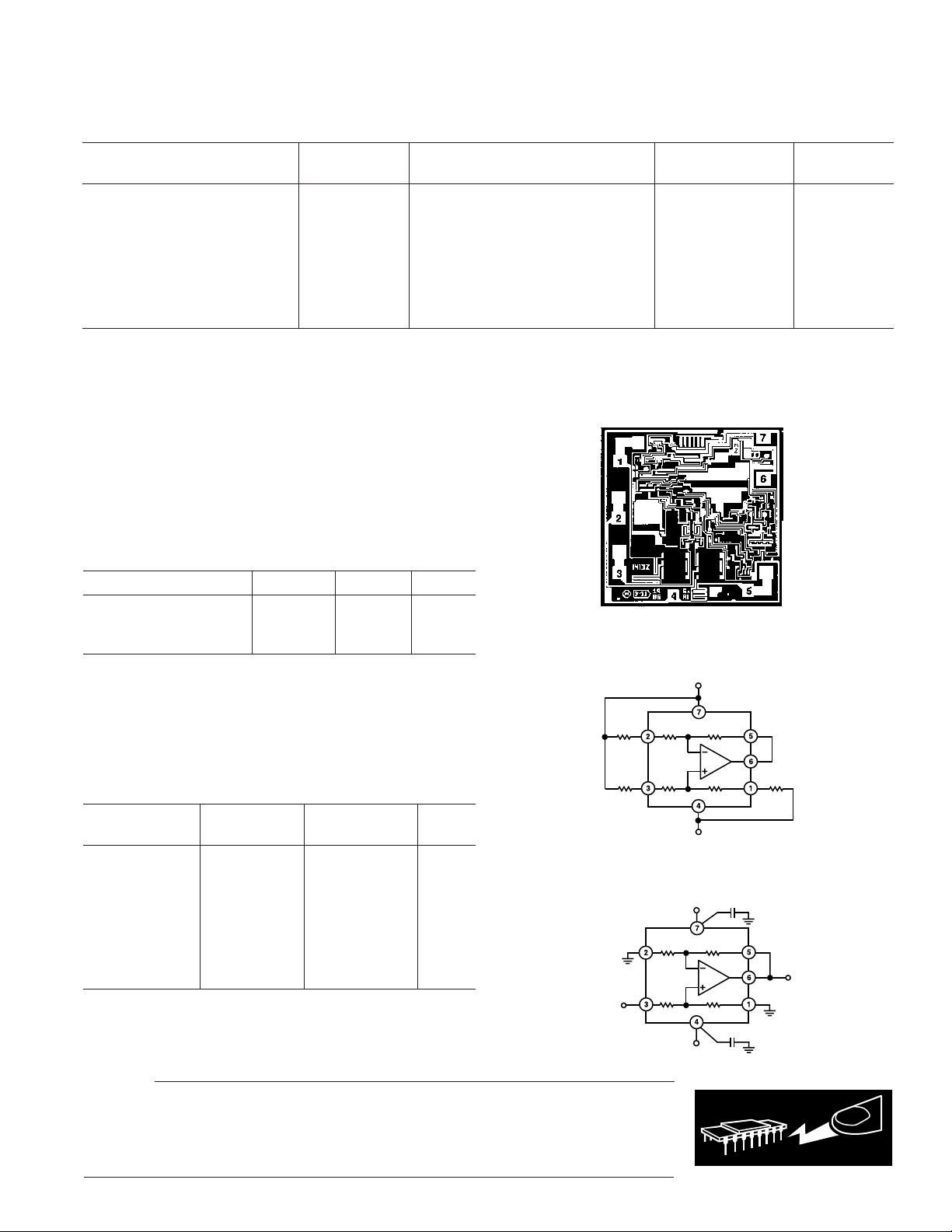
DIE SIZE 0.076 inch ⴛ 0.076 inch, 5,776 sq. mm
(1.93 mm ⴛ 1.93 mm, 3.73 sq. mm)
WAFER TEST LIMITS
(@ VS = ⴞ15 V, TA = 25ⴗC, unless otherwise noted.)*
AMP03GBC
Parameter Symbol Conditions Limit Unit
Offset Voltage V
OS
Gain Error No Load, V
VS = ± 18 V 0.5 mV max
= ± 10 V, RS = 0 Ω 0.008 % max
IN
Input Voltage Range IVR ± 10 V min
Common-Mode Rejection CMR V
Power Supply Rejection Ratio PSRR V
Output Swing V
Short-Circuit Current Limit I
Supply Current I
*Electrical tests are performed at wafer probe to the limits shown. Due to variations in assembly methods and normal yield loss, yield after packaging is not guaranteed
for standard product dice. Consult factory to negotiate specifications based on dice lot qualifications through sample lot assembly and testing.
ABSOLUTE MAXIMUM RATINGS
Supply Voltage . . . . . . . . . . . . . . . . . . . . . . . . . . . . . . . ± 18 V
Input Voltage
2
. . . . . . . . . . . . . . . . . . . . . . . . . Supply Voltage
O
SC
SY
1
= ± 10 V 80 dB min
CM
= ± 6 V to ± 18 V 8 µV/V max
S
RL = 2 kΩ±12 V max
Output Shorted to Ground +45/–15 mA min
No Load 3.5 mA max
DICE CHARACTERISTICS
Output Short-Circuit Duration . . . . . . . . . . . . . . Continuous
Storage Temperature Range
P, J Package . . . . . . . . . . . . . . . . . . . . . . . –65°C to +150°C
Lead Temperature (Soldering, 60 sec) . . . . . . . . . . . . 300°C
Junction Temperature . . . . . . . . . . . . . . . . . . . . . . . . . 150°C
Operating Temperature Range
AMP03B . . . . . . . . . . . . . . . . . . . . . . . . . –55°C to +125°C
AMP03F, AMP03G . . . . . . . . . . . . . . . . . . –40°C to +85°C
Package Type
3
JA
JC
Unit
Header (J) 150 18 °C/W
8-Lead PDIP (P) 103 43 °C/W
8-Lead SOIC (S) 155 40 °C/W
NOTES
1
Absolute maximum ratings apply to both DICE and packaged parts, unless
otherwise noted.
2
For supply voltages less than ± 18 V, the absolute maximum input voltage is equal
to the supply voltage.
3
θJA is specified for worst-case mounting conditions, i.e., θJA is specified for device
in socket for header and PDIP packages and for device soldered to printed circuit
board for SOIC package.
BURN-IN CIRCUIT
25k⍀
+18V
AMP03
25k⍀25k⍀
ORDERING GUIDE
1
Model
AMP03GP –40°C to +85°C8-Lead PDIP P-8
AMP03BJ –40°C to +85°CHeader H-08B
AMP03FJ –40°C to +85°CHeader H-08B
AMP03BJ/883C –55°C to +125°CHeader H-08B
AMP03GS –40°C to +85°C8-Lead SOIC S-8
AMP03GS-REEL –40°C to +85°C8-Lead SOIC S-8
Temperature Package Package
Range Description Option
2
SLEW RATE TEST CIRCUIT
–18V
+15V
0.1F
AMP03
5962-9563901MGA –55°C to +125°CHeader H-08B
= ⴞ10V
AMP03GBC Die
NOTES
1
Burn-in is available on commercial and industrial temperature range parts in
PDIP and header packages.
2
Consult factory for /883 data sheet.
CAUTION
ESD (electrostatic discharge) sensitive device. Electrostatic charges as high as 4000 V readily
accumulate on the human body and test equipment and can discharge without detection.
Although the AMP03 features proprietary ESD protection circuitry, permanent damage may
occur on devices subjected to high energy electrostatic discharges. Therefore, proper ESD
VIN = ⴞ10V
precautions are recommended to avoid performance degradation or loss of functionality.
0.1F
–15V
WARNING!
V
OUT
ESD SENSITIVE DEVICE
REV. F
–3–
 Loading...