Analog Devices AMP02GBC, AMP02FS-REEL, AMP02FS, AMP02FP, AMP02EP Datasheet
...
High Accuracy 8-Pin
a
FEATURES
Low Offset Voltage: 100 mV max
Low Drift: 2 mV/8C max
Wide Gain Range 1 to 10,000
High Common-Mode Rejection: 115 dB min
High Bandwidth (G = 1000): 200 kHz typ
Gain Equation Accuracy: 0.5% max
Single Resistor Gain Set
Input Overvoltage Protection
Low Cost
Available In Die Form
APPLICATIONS
Differential Amplifier
Strain Gauge Amplifier
Thermocouple Amplifier
RTD Amplifier
Programmable Gain Instrumentation Amplifier
Medical Instrumentation
Data Acquisition Systems
Instrumentation Amplifier
AMP02
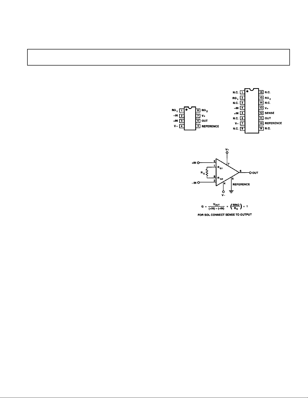
PIN CONNECTIONS
Epoxy Mini-DIP 16-Pin SOL
(P Suffix) (S Suffix)
and
Cerdip
(Z Suffix)
NC = NO CONNECT
GENERAL DESCRIPTION
The AMP02 is the first precision instrumentation amplifier
available in an 8-pin package. Gain of the AMP02 is set by a
single external resistor, and can range from 1 to 10,000. No
gain set resistor is required for unity gain. The AMP02 includes
an input protection network that allows the inputs to be taken
60 V beyond either supply rail without damaging the device.
Laser trimming reduces the input offset voltage to under 100 µV.
Output offset voltage is below 4 mV and gain accuracy is better
than 0.5% for gain of 1000. PMI’s proprietary thin-film resistor
process keeps the gain temperature coefficient under 50 ppm/°C.
Due to the AMP02’s design, its bandwidth remains very high
over a wide range of gain. Slew rate is over 4 V/µs making the
AMP02 ideal for fast data acquisition systems.
Figure 1. Basic Circuit Connections
A reference pin is provided to allow the output to be referenced
to an external dc level. This pin may be used for offset correction or level shifting as required. In the 8-pin package, sense is
internally connected to the output.
For an instrumentation amplifier with the highest precision,
consult the AMP01 data sheet. For the highest input impedance
and speed, consult the AMP05 data sheet.
REV. D
Information furnished by Analog Devices is believed to be accurate and
reliable. However, no responsibility is assumed by Analog Devices for its
use, nor for any infringements of patents or other rights of third parties
which may result from its use. No license is granted by implication or
otherwise under any patent or patent rights of Analog Devices.
One Technology Way, P.O. Box 9106, Norwood, MA 02062-9106, U.S.A.
Tel: 617/329-4700 Fax: 617/326-8703

AMP02–SPECIFICA TIONS
ELECTRICAL CHARACTERISTICS
(@ VS = 615 V, VCM = 0 V, TA = +258C, unless otherwise noted.)
AMP02E AMP02F
Parameter Symbol Conditions Min Typ Max Min Typ Max Units
OFFSET VOLTAGE
Input Offset Voltage V
Input Offset Voltage Drift TCV
Output Offset Voltage V
Output Offset Voltage Drift TCV
Power Supply Rejection PSR VS = ±4.8 V to ±18 V
IOS
IOS
OOS
OOS
TA = +25°C 20 100 40 200 µV
–40°C ≤ TA ≤ +85°C 50 200 100 350 µV
–40°C ≤ TA ≤ +85°C 0.5 2 1 4 µV/°C
TA = +25°C1428mV
–40°C ≤ TA ≤ +85°C410920mV
–40°C ≤ TA ≤ +85°C 50 100 100 200 µV/°C
G = 100, 1000 115 125 110 115 dB
G = 10 100 110 95 100 dB
G = 1 80 90 75 80 dB
VS = ±4.8 V to ±18 V
–40°C ≤ TA ≤ +85°C
G = 1000, 100 110 120 105 110 dB
G = 10 95 110 90 95 dB
G = 1 75 90 70 75 dB
INPUT CURRENT
Input Bias Current I
Input Bias Current Drift TCI
Input Offset Current I
Input Offset Current Drift TCI
B
OS
B
OS
TA = +25°C210420nA
–40°C ≤ TA ≤ +85°C 150 250 pA/°C
TA = +25°C 1.2 5 2 10 nA
–40°C ≤ TA ≤ +85°C 9 15 pA/ °C
INPUT
Input Resistance R
IN
Differential, G ≤ 1000 10 10 GΩ
Common-Mode, G = 1000 16.5 16.5 GΩ
Input Voltage Range IVR TA = +25°C (Note 1) ±11 ±11 V
Common-Mode Rejection CMR V
= ±11 V
CM
G = 1000, 100 115 120 110 115 dB
G = 10 100 115 95 110 dB
G = 1 80 95 75 90 dB
VCM = ±11 V
–40°C ≤ TA ≤ +85°C
G = 100, 1000 110 120 105 115 dB
G = 10 95 110 90 105 dB
G = 1 75 90 70 85 dB
GAIN
Gain Equation G = 1000 0.50 0.70 %
Accuracy G =
50 kΩ
+1 G = 100 0.30 0.50 %
R
G
G = 10 0.25 0.40 %
G = 1 0.02 0.05 %
Gain Range G 1 10k 1 10k V/V
Nonlinearity G = 1 to 1000 0.006 0.006 %
Temperature Coefficient G
TC
1 ≤ G ≤ 1000 (Notes 2, 3) 20 50 20 50 ppm/°C
OUTPUT RATING
Output Voltage Swing V
OUT
Positive Current Limit Output-to-Ground Short 22 22 mA
TA = +25°C, RL = 1 kΩ±12 ±13 ±12 ±13 V
R
= 1 kΩ, –40°C ≤ TA ≤ +85°C ±11 ±12 ±11 ±12 V
L
Negative Current Limit Output-to-Ground Short 32 32 mA
NOISE
Voltage Density, RTI e
n
fO = 1 kHz
G = 1000 9 9 nV/√Hz
G = 100 10 10 nV/√Hz
G = 10 18 18 nV/√Hz
G = 1 120 120 nV/√Hz
Noise Current Density, RTI i
Input Noise Voltage en p-p 0.1 Hz to 10 Hz
n
fO = 1 kHz, G = 1000 0.4 0.4 pA/√Hz
G = 1000 0.4 0.4 µV p-p
G = 100 0.5 0.5 µV p-p
G = 10 1.2 1.2 µV p-p
DYNAMIC RESPONSE
Small-Signal Bandwidth BW G = 1 1200 1200 kHz
(–3 dB) G = 10 300 300 kHz
G = 100, 1000 200 200 kHz
Slew Rate SR G = 10, RL = 1 kΩ 46 4 6 V/µs
Settling Time t
S
To 0.01% ±10 V Step
G = 1 to 1000 10 10 µs
SENSE INPUT
Input Resistance R
Voltage Range ± 11 ±11 V
IN
25 25 kΩ
REFERENCE INPUT
Input Resistance R
Voltage Range ± 11 ± 11 V
IN
50 50 kΩ
Gain to Output 1 1 V/V
–2–
REV. D

AMP02
AMP02E AMP02F
Parameter Symbol Conditions Min Typ Max Min Typ Max Units
POWER SUPPLY
Supply Voltage Range V
Supply Current I
NOTES
1
Input voltage range guaranteed by common-mode rejection test.
2
Guaranteed by design.
3
Gain tempco does not include the effects of external component drift.
Specifications subject to change without notice.
S
SY
TA = +25°C5656mA
–40°C ≤ TA ≤ +85°C5656mA
±4.5 ±18 ±4.5 ±18 V
ABSOLUTE MAXIMUM RATINGS
Supply Voltage . . . . . . . . . . . . . . . . . . . . . . . . . . . . . . . . ±18 V
Common-Mode Input Voltage .[(V–) – 60 V] to [(V+) + 60 V]
Differential Input Voltage . . . .[(V–) – 60 V] to [(V+) + 60 V]
Output Short-Circuit Duration . . . . . . . . . . . . . . .Continuous
Operating Temperature Range . . . . . . . . . . . . –40°C to +85°C
Storage Temperature Range . . . . . . . . . . . . –65°C to +150°C
Function Temperature Range . . . . . . . . . . . –65°C to +150°C
Lead Temperature (Soldering, 10 sec) . . . . . . . . . . . . +300°C
ORDERING GUIDE
V
max @ V
Model TA = +258CTA = +258C Range Description
AMP02EP 100 µV 4 mV –40°C to +85°C 8-Pin Plastic DIP
AMP02FP 200 µV 8 mV –40°C to +85°C 8-Pin Plastic DIP
AMP02AZ/883C 200 µV 10 mV –55°C to +125°C 8-Pin Cerdip
AMP02FS 200 µV 8 mV –40°C to +85°C 16-Pin SOIC
AMP02GBC Die
AMP02FS-REEL 200 µV 8 mV –40°C to +85°C 16-Pin SOIC
IOS
max @ Temperature Package
OOS
Package Type u
2
JA
u
JC
Units
8-Pin Plastic DIP (P) 96 37 °C/W
16-Pin SOL (S) 92 27 °C/W
NOTES
1
Absolute maximum ratings apply to both DICE and packaged parts, unless oth-
erwise noted.
2
θJA is specified for worst case mounting conditions, i.e., θJA is specified for de-
vice in socket for P-DIP package; θJA is specified for device soldered to printed
circuit board for SOL package.
REV. D
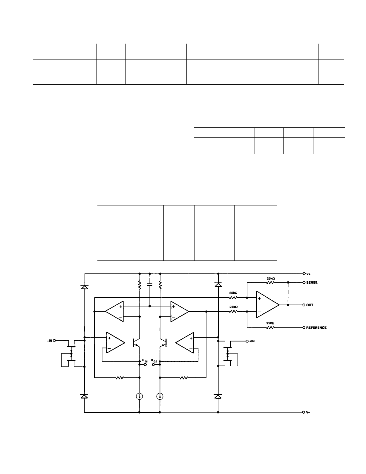
Figure 2. Simplified Schematic
–3–

AMP02
WARNING!
ESD SENSITIVE DEVICE
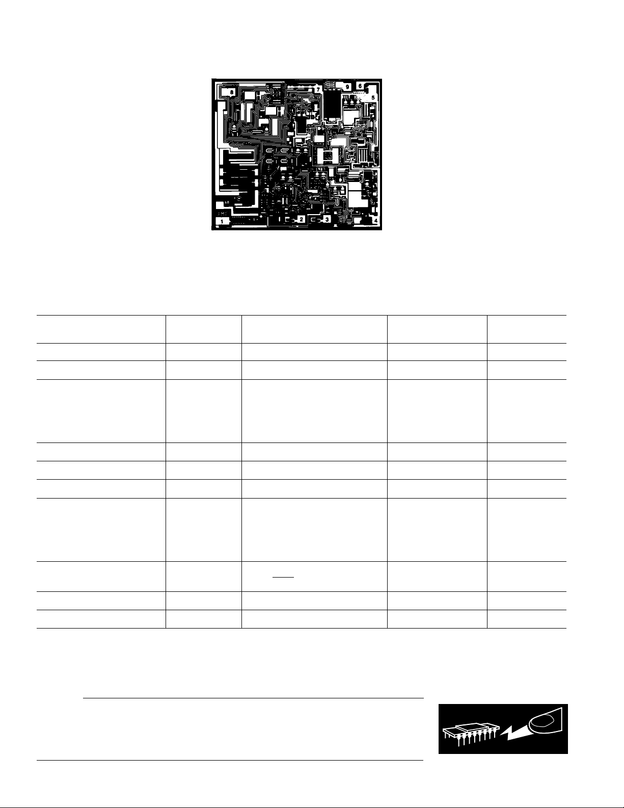
DIE SIZE 0.103 X 0.116 inch, 11,948 sq. mils
(2.62 X 2.95 mm, 7.73 sq. mm)
Dice Characteristics
1. RG
1
2. –IN
3. +IN
4. V–
5. REFERENCE
6. OUT
7. V+
8. RG
2
9. SENSE
CONNECT SUBSTRATE TO V–
WAFER TEST LIMITS
at VS = 615 V, VCM = 0 V, TA = +258C, unless otherwise noted.
AMP02 GBC
Parameter Symbol Conditions Limits Units
Input Offset Voltage V
Output Offset Voltage V
IOS
OOS
V
= ±4.8 V to ±18 V
S
200 µV max
8 mV max
G = 1000 110
Power Supply PSR G = 100 110 dB min
Rejection G = 10 95
G = 1 75
Input Bias Current I
Input Offset Current I
B
OS
20 nA max
10 nA max
Input Voltage Range IVR Guaranteed by CMR Tests ±11 V min
V
= ±11 V
CM
G = 1000 110
Common-Mode CMR G = 100 110 dB min
Rejection G = 10 95
G = 1 75
50 kΩ
Gain Equation Accuracy
Output Voltage Swing V
Supply Current I
NOTE
Electrical tests are performed at wafer probe to the limits shown. Due to variations in assembly methods and normal yield loss, yield after packaging is not guaranteed
for standard product dice. Consult factory to negotiate specifications based on dice lot qualifications through sample lot assembly and testing.
OUT
SY
G =
RL = 1 kΩ±12 V min
R
G
+1, G = 1000
0.7 % max
6 mA max
CAUTION
ESD (electrostatic discharge) sensitive device. Electrostatic charges as high as 4000 V readily
accumulate on the human body and test equipment and can discharge without detection.
Although the AMP02 features proprietary ESD protection circuitry, permanent damage may
occur on devices subjected to high energy electrostatic discharges. Therefore, proper ESD
precautions are recommended to avoid performance degradation or loss of functionality.
–4–
REV. D
 Loading...