ANALOG DEVICES ADXRS622 Service Manual

FEATURES
V
DD
AGND
PGND
AV
CC
ST2 ST1 TEMP V
RATIO
CP1 CP2 CP3 CP4 CP5 SUMJ RATEOUT
DEMOD
180kΩ ±1%
22nF
100nF
22n
F
100nF
100nF
100nF
DRIVE
AMP
MECHANICAL
SENSOR
CHARGE PUMP
AND VOLTAGE
REGULATOR
C
OUT
5V
5V
5V
(ADC REF)
AC
AMP
VGA
25kΩ
@ 25°C
ADXRS622
25kΩ
SELF-TEST
07754-001
http://www.BDTIC.com/ADI
Complete rate gyroscope on a single chip
Z-axis (yaw rate) response
High vibration rejection over wide frequency
2000 g powered shock survivability
Ratiometric to referenced supply
5 V single-supply operation
105°C operation
Self-test on digital command
Ultrasmall and light: <0.15 cc, <0.5 gram
Temperature sensor output
RoHS compliant
Qualified for automotive applications
APPLICATIONS
Vehicle chassis rollover sensing
Inertial measurement units
Platform stabilization
GENERAL DESCRIPTION
The ADXRS622 is a complete angular rate sensor (gyroscope)
that uses the Analog Devices, Inc., surface-micromachining
process to make a functionally complete and low cost angular
rate sensor, integrated with all of the required electronics on
one chip. The manufacturing technique for this device is the
same high volume BiMOS process used for high reliability
automotive airbag accelerometers.
The ADXRS622 is an automotive grade gyroscope that has
100% pin, package, temperature, and function compatible to the
available industrial grade ADXRS652 gyroscope. Automotive
grade gyroscopes have more extensive guaranteed minimum/
maximum specifications due to automotive testing.
The output signal, RATEOUT (1B, 2A), is a voltage proportional to
the angular rate about the axis that is normal to the top surface of
the package. The output is ratiometric with respect to a provided
reference supply. An external capacitor sets the bandwidth. Other
external capacitors are required for operation.
A temperature output is provided for compensation techniques.
Two digital self-test inputs electromechanically excite the sensor
to test proper operation of both the sensor and the signal conditioning circuits. The ADXRS622 is available in a 7 mm × 7 mm ×
3 mm BGA chip-scale package.
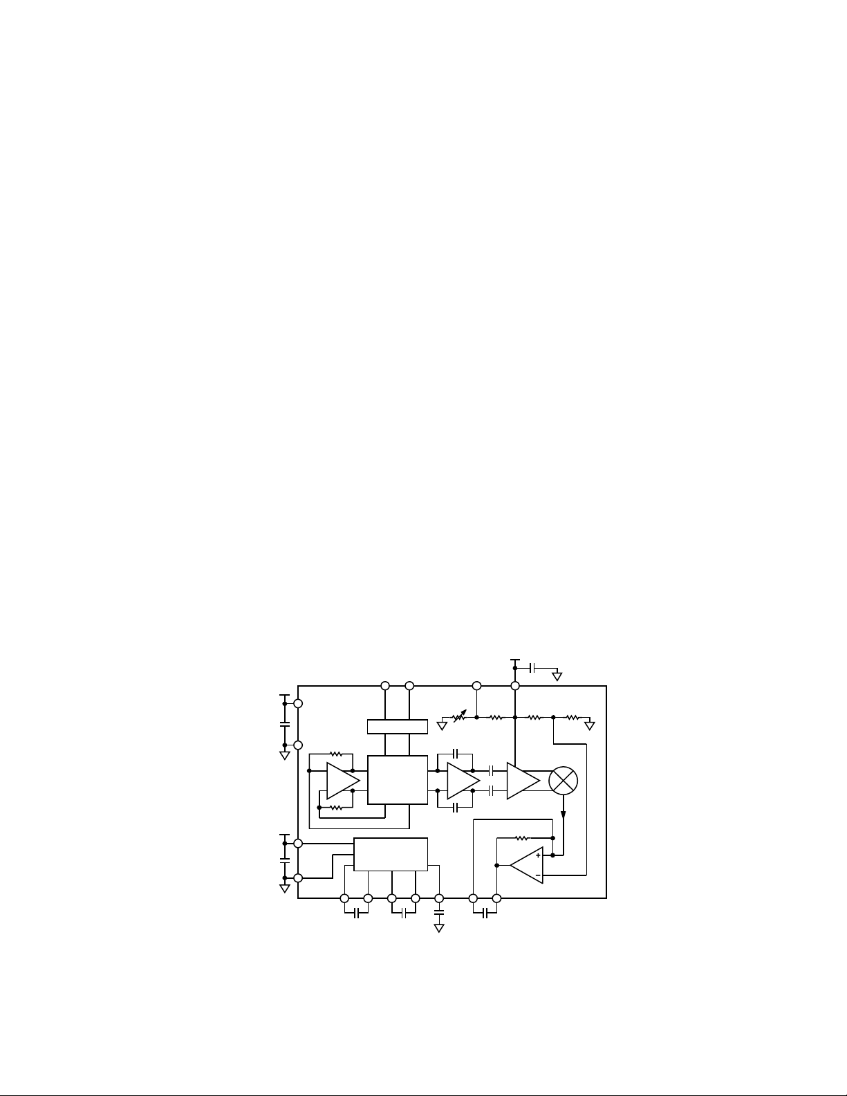
FUNCTIONAL BLOCK DIAGRAM
Figure 1.
 Loading...