

Analog Devices ADSP-2164KP-40, ADSP-2164BS-40, ADSP-2164BP-40, ADSP-2163KS-66, ADSP-2163KS-100 Datasheet
...
ADSP-2100 Family
EXTERNAL
ADDRESS
BUS
DATA
MEMORY
PROGRAM
MEMORY
EXTERNAL
DATA
BUS
ADSP-2100 CORE
ARITHMETIC UNITS
SHIFTER
MAC
ALU
MEMORY
SERIAL PORTS
SPORT 0 SPORT 1
HOST
INTERFACE
PORT
(ADSP-2111)
FLAGS
(ADSP-2111)
DATA ADDRESS
GENERATORS
DAG 1
DAG 2
PROGRAM
SEQUENCER
PROGRAM MEMORY ADDRESS
DATA MEMORY ADDRESS
PROGRAM MEMORY DATA
DATA MEMORY DATA
TIMER
a
SUMMARY
16-Bit Fixed-Point DSP Microprocessors with
On-Chip Memory
Enhanced Harvard Architecture for Three-Bus
Performance: Instruction Bus & Dual Data Buses
Independent Computation Units: ALU, Multiplier/
Accumulator, and Shifter
Single-Cycle Instruction Execution & Multifunction
Instructions
On-Chip Program Memory RAM or ROM
& Data Memory RAM
Integrated I/O Peripherals: Serial Ports, Timer,
Host Interface Port (ADSP-2111 Only)
FEATURES
25 MIPS, 40 ns Maximum Instruction Rate
Separate On-Chip Buses for Program and Data Memory
Program Memory Stores Both Instructions and Data
(Three-Bus Performance)
Dual Data Address Generators with Modulo and
Bit-Reverse Addressing
Efficient Program Sequencing with Zero-Overhead
Looping: Single-Cycle Loop Setup
Automatic Booting of On-Chip Program Memory from
Byte-Wide External Memory (e.g., EPROM )
Double-Buffered Serial Ports with Companding Hardware,
Automatic Data Buffering, and Multichannel Operation
ADSP-2111 Host Interface Port Provides Easy Interface
to 68000, 80C51, ADSP-21xx, Etc.
Automatic Booting of ADSP-2111 Program Memory
Through Host Interface Port
Three Edge- or Level-Sensitive Interrupts
Low Power IDLE Instruction
PGA, PLCC, PQFP, and TQFP Packages
MIL-STD-883B Versions Available
GENERAL DESCRIPTION
The ADSP-2100 Family processors are single-chip microcomputers optimized for digital signal processing(DSP)
and other high speed numeric processing applications. The
ADSP-21xx processors are all built upon a common core. Each
processor combines the core DSP architecture—computation
units, data address generators, and program sequencer—with
differentiating features such as on-chip program and data
memory RAM, a programmable timer, one or two serial ports,
and, on the ADSP-2111, a host interface port.
REV. B
Information furnished by Analog Devices is believed to be accurate and
reliable. However, no responsibility is assumed by Analog Devices for its
use, nor for any infringements of patents or other rights of third parties
which may result from its use. No license is granted by implication or
otherwise under any patent or patent rights of Analog Devices.
DSP Microcomputers
ADSP-21xx
FUNCTIONAL BLOCK DIAGRAM
This data sheet describes the following ADSP-2100 Family
processors:
ADSP-2101
ADSP-2103 3.3 V Version of ADSP-2101
ADSP-2105 Low Cost DSP
ADSP-2111 DSP with Host Interface Port
ADSP-2115
ADSP-2161/62/63/64 Custom ROM-programmed DSPs
The following ADSP-2100 Family processors are not included
in this data sheet:
ADSP-2100A DSP Microprocessor
ADSP-2165/66 ROM-programmed ADSP-216x processors
with powerdown and larger on-chip
memories (12K Program Memory ROM,
1K Program Memory RAM, 4K Data
Memory RAM)
ADSP-21msp5x Mixed-Signal DSP Processors with
integrated on-chip A/D and D/A plus
powerdown
ADSP-2171 Speed and feature enhanced ADSP-2100
Family processor with host interface port,
powerdown, and instruction set extensions
for bit manipulation, multiplication, biased
rounding, and global interrupt masking
ADSP-2181 ADSP-21xx processor with ADSP-2171
features plus 80K bytes of on-chip RAM
configured as 16K words of program
memory and 16K words of data memory.
Refer to the individual data sheet of each of these processors for
further information.
© Analog Devices, Inc., 1996
One Technology Way, P.O. Box 9106, Norwood, MA 02062-9106, U.S.A.
Tel: 617/329-4700 Fax: 617/326-8703

ADSP-21xx
Fabricated in a high speed, submicron, double-layer metal
CMOS process, the highest-performance ADSP-21xx processors operate at 25 MHz with a 40 ns instruction cycle time.
Every instruction can execute in a single cycle. Fabrication in
CMOS results in low power dissipation.
The ADSP-2100 Family’s flexible architecture and comprehensive instruction set support a high degree of parallelism.
In one cycle the ADSP-21xx can perform all of thefollowing
operations:
•
Generate the next program address
•
Fetch the next instruction
•
Perform one or two data moves
•
Update one or two data address pointers
•
Perform a computation
TABLE OF CONTENTS
GENERAL DESCRIPTION . . . . . . . . . . . . . . . . . . . . . . . . 1
Development Tools . . . . . . . . . . . . . . . . . . . . . . . . . . . . . . . 4
Additional Information . . . . . . . . . . . . . . . . . . . . . . . . . . . . 4
ARCHITECTURE OVERVIEW . . . . . . . . . . . . . . . . . . . . 4
Serial Ports . . . . . . . . . . . . . . . . . . . . . . . . . . . . . . . . . . . . . 5
Host Interface Port (ADSP-2111) . . . . . . . . . . . . . . . . . . . . 6
Interrupts . . . . . . . . . . . . . . . . . . . . . . . . . . . . . . . . . . . . . . . 6
Pin Definitions . . . . . . . . . . . . . . . . . . . . . . . . . . . . . . . . . . . 7
SYSTEM INTERFACE . . . . . . . . . . . . . . . . . . . . . . . . . . . 7
Clock Signals . . . . . . . . . . . . . . . . . . . . . . . . . . . . . . . . . . . . 7
Reset . . . . . . . . . . . . . . . . . . . . . . . . . . . . . . . . . . . . . . . . . . 8
Program Memory Interface . . . . . . . . . . . . . . . . . . . . . . . . 10
Program Memory Maps . . . . . . . . . . . . . . . . . . . . . . . . . . . 10
Data Memory Interface . . . . . . . . . . . . . . . . . . . . . . . . . . . 12
Data Memory Map . . . . . . . . . . . . . . . . . . . . . . . . . . . . . . 12
Boot Memory Interface . . . . . . . . . . . . . . . . . . . . . . . . . . . 12
Bus Interface . . . . . . . . . . . . . . . . . . . . . . . . . . . . . . . . . . . 12
Low Power IDLE Instruction . . . . . . . . . . . . . . . . . . . . . . 13
ADSP-216x Prototyping . . . . . . . . . . . . . . . . . . . . . . . . . . 13
Ordering Procedure for ADSP-216x ROM Processors . . . . 13
Wafer Products . . . . . . . . . . . . . . . . . . . . . . . . . . . . . . . . . 14
Functional Differences for Older Revision Devices . . . . . . 14
Instruction Set . . . . . . . . . . . . . . . . . . . . . . . . . . . . . . . . . . 15
SPECIFICATIONS
(ADSP-2101/2105/2115/2161/2163) . . . . . . . . . . . . . . . 17
Recommended Operating Conditions . . . . . . . . . . . . . . . . 17
Electrical Characteristics . . . . . . . . . . . . . . . . . . . . . . . . . . 17
Supply Current & Power (ADSP-2101/2161/2163) . . . . . . 18
Power Dissipation Example . . . . . . . . . . . . . . . . . . . . . . . . 19
Environmental Conditions . . . . . . . . . . . . . . . . . . . . . . . . . 19
Capacitive Loading . . . . . . . . . . . . . . . . . . . . . . . . . . . . . . 19
Test Conditions . . . . . . . . . . . . . . . . . . . . . . . . . . . . . . . . . 20
SPECIFICATIONS
(ADSP-2111) . . . . . . . . . . . . . . . . . . . . . . . . . . . . . . . . . 21
Recommended Operating Conditions . . . . . . . . . . . . . . . . 21
Electrical Characteristics . . . . . . . . . . . . . . . . . . . . . . . . . . 21
Supply Current & Power . . . . . . . . . . . . . . . . . . . . . . . . . . 22
Power Dissipation Example . . . . . . . . . . . . . . . . . . . . . . . . 23
Environmental Conditions . . . . . . . . . . . . . . . . . . . . . . . . . 23
•
Receive and transmit data via one or two serial ports
•
Receive and/or transmit data via the host interface port
(ADSP-2111 only)
The ADSP-2101, ADSP-2105, and ADSP-2115 comprise the
basic set of processors of the family. Each of these three devices
contains program and data memory RAM, an interval timer,
and one or two serial ports. The ADSP-2103 is a 3.3 volt
power supply version of the ADSP-2101; it is identical to the
ADSP-2101 in all other characteristics. Table I shows the
features of each ADSP-21xx processor.
The ADSP-2111 adds a 16-bit host interface port (HIP) to the
basic set of ADSP-21xx integrated features. The host port
provides a simple interface to host microprocessors or
microcontrollers such as the 8031, 68000, or ISA bus.
Capacitive Loading . . . . . . . . . . . . . . . . . . . . . . . . . . . . . . 23
Test Conditions . . . . . . . . . . . . . . . . . . . . . . . . . . . . . . . . . 24
SPECIFICATIONS (ADSP-2103/2162/2164) . . . . . . . . . 25
Recommended Operating Conditions . . . . . . . . . . . . . . . . 25
Electrical Characteristics . . . . . . . . . . . . . . . . . . . . . . . . . . 25
Supply Current & Power . . . . . . . . . . . . . . . . . . . . . . . . . . 26
Power Dissipation Example . . . . . . . . . . . . . . . . . . . . . . . . 27
Environmental Conditions . . . . . . . . . . . . . . . . . . . . . . . . . 27
Capacitive Loading . . . . . . . . . . . . . . . . . . . . . . . . . . . . . . 27
Test Conditions . . . . . . . . . . . . . . . . . . . . . . . . . . . . . . . . . 28
TIMING PARAMETERS
(ADSP-2101/2105/2111/2115/2161/2163) . . . . . . . . . . . . 29
Clock Signals . . . . . . . . . . . . . . . . . . . . . . . . . . . . . . . . . . . 30
Interrupts & Flags . . . . . . . . . . . . . . . . . . . . . . . . . . . . . . . 31
Bus Request–Bus Grant . . . . . . . . . . . . . . . . . . . . . . . . . . . 32
Memory Read . . . . . . . . . . . . . . . . . . . . . . . . . . . . . . . . . . 33
Memory Write . . . . . . . . . . . . . . . . . . . . . . . . . . . . . . . . . . 34
Serial Ports . . . . . . . . . . . . . . . . . . . . . . . . . . . . . . . . . . . . 35
Host Interface Port (ADSP-2111) . . . . . . . . . . . . . . . . . . . 36
TIMING PARAMETERS (ADSP-2103/2162/2164) . . . . 44
Clock Signals . . . . . . . . . . . . . . . . . . . . . . . . . . . . . . . . . . . 45
Interrupts & Flags . . . . . . . . . . . . . . . . . . . . . . . . . . . . . . . 46
Bus Request–Bus Grant . . . . . . . . . . . . . . . . . . . . . . . . . . . 47
Memory Read . . . . . . . . . . . . . . . . . . . . . . . . . . . . . . . . . . 48
Memory Write . . . . . . . . . . . . . . . . . . . . . . . . . . . . . . . . . . 49
Serial Ports . . . . . . . . . . . . . . . . . . . . . . . . . . . . . . . . . . . . 50
PIN CONFIGURATIONS
68-Pin PGA (ADSP-2101) . . . . . . . . . . . . . . . . . . . . . . . . 51
68-Lead PLCC (ADSP-2101/2103/2105/2115/216x) . . . . 52
80-Lead PQFP (ADSP-2101/2103/2115/216x) . . . . . . . . . 53
80-Lead TQFP (ADSP-2115) . . . . . . . . . . . . . . . . . . . . . . 53
100-Pin PGA (ADSP-2111) . . . . . . . . . . . . . . . . . . . . . . . 54
100-Lead PQFP (ADSP-2111) . . . . . . . . . . . . . . . . . . . . . 55
PACKAGE OUTLINE DIMENSIONS
68-Pin PGA . . . . . . . . . . . . . . . . . . . . . . . . . . . . . . . . . . . . 56
68-Lead PLCC . . . . . . . . . . . . . . . . . . . . . . . . . . . . . . . . . 57
80-Lead PQFP, 80-Lead TQFP . . . . . . . . . . . . . . . . . . . . 58
100-Pin PGA . . . . . . . . . . . . . . . . . . . . . . . . . . . . . . . . . . . 59
100-Lead PQFP . . . . . . . . . . . . . . . . . . . . . . . . . . . . . . . . 60
ORDERING GUIDE . . . . . . . . . . . . . . . . . . . . . . . . . .61-62
–2–
REV. B
Table I. ADSP-21xx Processor Features
Feature 2101 2103 2105 2115 2111
Data Memory (RAM) 1K 1K
Program Memory (RAM) 2K 2K 1K 1K 2K
Timer
Serial Port 0 (Multichannel)
Serial Port 1
Host Interface Port – – – –
Speed Grades (Instruction Cycle Time)
10.24 MHz (76.9 ns) –
13.0 MHz (76.9 ns) – – – –
13.824 MHz (72.3 ns) – –
16.67 MHz (60 ns)
20.0 MHz (50 ns)
25 MHz (40 ns)
Supply Voltage 5 V 3.3 V 5 V 5 V 5 V
Packages
68-Pin PGA
68-Lead PLCC
80-Lead PQFP
80-Lead TQFP – – –
100-Pin PGA – – – –
100-Lead PQFP – – – –
Temperature Grades
K Commercial 0°C to +70°C
B Industrial –40°C to +85°C
T Extended –55°C to +125°C
•••••
••
•••••
•
•
•
•
•
– –
–
– –
– – – –
••••
••
•••••
•••••
•
– – –
1
⁄2K
–
– – –
•
•••
–
1
⁄2K1K
••
•
– –
•
••
•
•
•
–
–
–
–
•
•
•
ADSP-21xx
Table II. ADSP-216x ROM-Programmed Processor Features
Feature 2161 2162 2163 2164
Data Memory (RAM)
Program Memory (ROM) 8K 8K 4K 4K
Program Memory (RAM) – – – –
Timer
Serial Port 0 (Multichannel)
Serial Port 1
Supply Voltage 5 V 3.3 V 5 V 3.3 V
Speed Grades (Instruction Cycle Time)
10.24 MHz (97.6 ns) –
16.67 MHz (60 ns)
25 MHz (40 ns) ––
Packages
68-Lead PLCC
80-Lead PQFP
Temperature Grades
K Commercial 0°C to +70°C
B Industrial –40°C to +85°C
1
⁄2K
••••
••••
••••
•
••••
••••
••••
••••
1
•
–
⁄2K
1
⁄2K
–
•
•
1
⁄2K
•
–
–
REV. B
–3–

ADSP-21xx
The ADSP-216x series are memory-variant versions of the
ADSP-2101 and ADSP-2103 that contain factory-programmed
on-chip ROM program memory. These devices offer different
amounts of on-chip memory for program and data storage.
Table II shows the features available in the ADSP-216x series of
custom ROM-coded processors.
The ADSP-216x products eliminate the need for an external
boot EPROM in your system, and can also eliminate the need
for any external program memory by fitting the entire application program in on-chip ROM. These devices thus provide an
excellent option for volume applications where board space and
system cost constraints are of critical concern.
Development Tools
The ADSP-21xx processors are supported by a complete set of
tools for system development. The ADSP-2100 Family Development Software includes C and assembly language tools that
allow programmers to write code for any of the ADSP-21xx
processors. The ANSI C compiler generates ADSP-21xx
assembly source code, while the runtime C library provides
ANSI-standard and custom DSP library routines. The ADSP21xx assembler produces object code modules which the linker
combines into an executable file. The processor simulators
provide an interactive instruction-level simulation with a
reconfigurable, windowed user interface. A PROM splitter
utility generates PROM programmer compatible files.
EZ-ICE
®
in-circuit emulators allow debugging of ADSP-21xx
systems by providing a full range of emulation functions such as
modification of memory and register values and execution
breakpoints. EZ-LAB
®
demonstration boards are complete DSP
systems that execute EPROM-based programs.
The EZ-Kit Lite is a very low-cost evaluation/development
platform that contains both the hardware and software needed
to evaluate the ADSP-21xx architecture.
Additional details and ordering information is available in the
ADSP-2100 Family Software & Hardware Development Tools data
sheet (ADDS-21xx-TOOLS). This data sheet can be requested
from any Analog Devices sales office or distributor.
Additional Information
This data sheet provides a general overview of ADSP-21xx
processor functionality. For detailed design information on the
architecture and instruction set, refer to the ADSP-2100 Family
User’s Manual, available from Analog Devices.
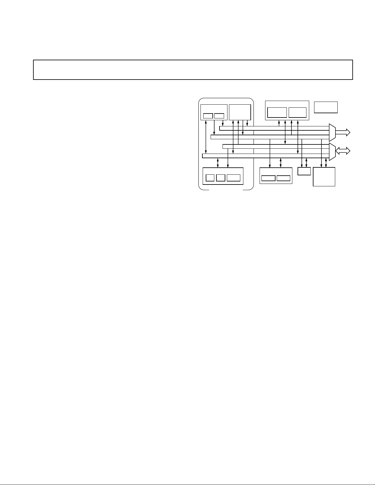
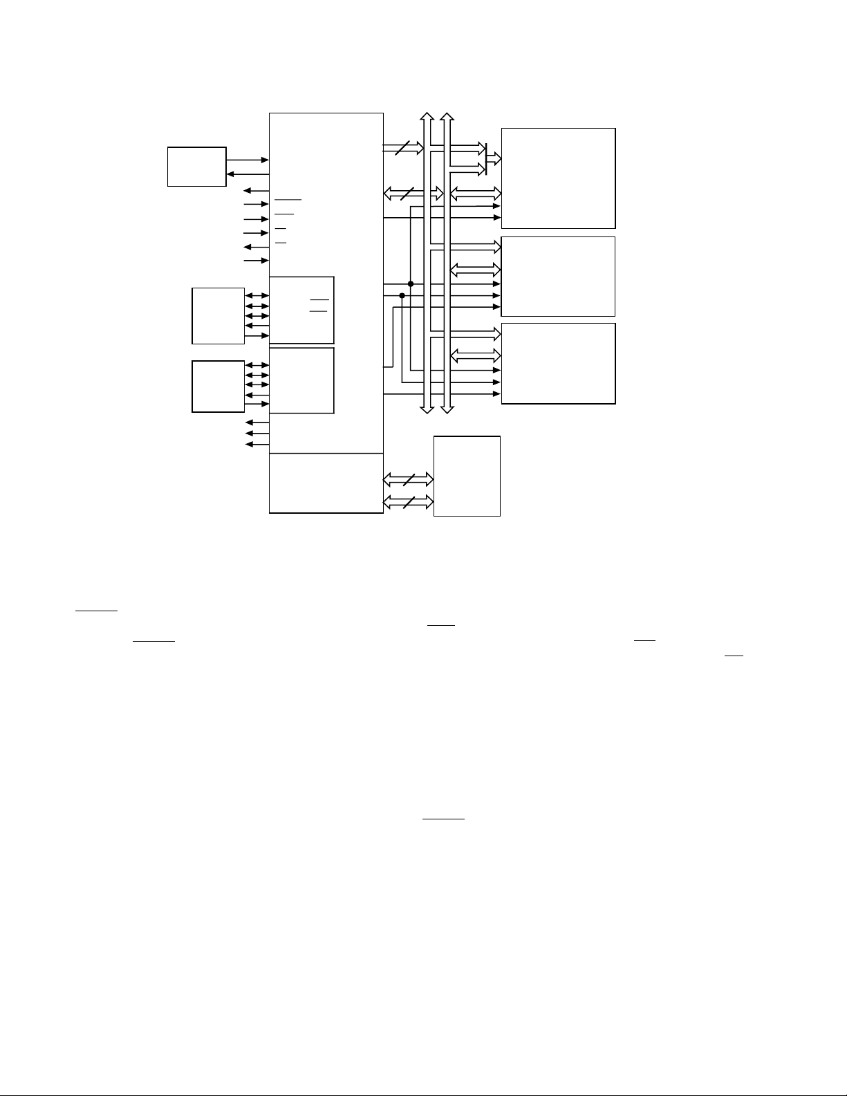
ARCHITECTURE OVERVIEW
Figure 1 shows a block diagram of the ADSP-21xx architecture.
The processors contain three independent computational units:
the ALU, the multiplier/accumulator (MAC), and the shifter.
The computational units process 16-bit data directly and have
provisions to support multiprecision computations. The ALU
performs a standard set of arithmetic and logic operations;
division primitives are also supported. The MAC performs
single-cycle multiply, multiply/add, and multiply/subtract
operations. The shifter performs logical and arithmetic shifts,
normalization, denormalization, and derive exponent operations.
The shifter can be used to efficiently implement numeric format
control including multiword floating-point representations.
The internal result (R) bus directly connects the computational
units so that the output of any unit may be used as the input of
any unit on the next cycle.
A powerful program sequencer and two dedicated data address
generators ensure efficient use of these computational units.
The sequencer supports conditional jumps, subroutine calls,
and returns in a single cycle. With internal loop counters and
loop stacks, the ADSP-21xx executes looped code with zero
overhead—no explicit jump instructions are required to
maintain the loop.
Two data address generators (DAGs) provide addresses for
simultaneous dual operand fetches (from data memory and
program memory). Each DAG maintains and updates four
address pointers. Whenever the pointer is used to access data
(indirect addressing), it is post-modified by the value of one of
four modify registers. A length value may be associated with
each pointer to implement automatic modulo addressing for
circular buffers. The circular buffering feature is also used by
the serial ports for automatic data transfers to (and from) onchip memory.
Efficient data transfer is achieved with the use of five internal
buses:
• Program Memory Address (PMA) Bus
• Program Memory Data (PMD) Bus
• Data Memory Address (DMA) Bus
• Data Memory Data (DMD) Bus
• Result (R) Bus
The two address buses (PMA, DMA) share a single external
address bus, allowing memory to be expanded off-chip, and the
two data buses (PMD, DMD) share a single external data bus.
The
BMS, DMS, and PMS signals indicate which memory
space is using the external buses.
Program memory can store both instructions and data, permit-
ting the ADSP-21xx to fetch two operands in a single cycle, one
from program memory and one from data memory. The
processor can fetch an operand from on-chip program memory
and the next instruction in the same cycle.
The memory interface supports slow memories and memorymapped peripherals with programmable wait state generation.
External devices can gain control of the processor’s buses with
the use of the bus request/grant signals (
BR, BG).
EZ-ICE and EZ-LAB are registered trademarks of Analog Devices, Inc.
–4–
REV. B
ADSP-21xx
DATA
ADDRESS
GENERATOR
#1
INPUT REGS
ALU
OUTPUT REGS
DATA
ADDRESS
GENERATOR
#2
PMD BUS
24
DMD BUS
16
PMA BUS
14
14
DMA BUS
INPUT REGS
MAC
OUTPUT REGS
INSTRUCTION
REGISTER
PROGRAM
SEQUENCER
INPUT REGS
SHIFTER
OUTPUT REGS
PROGRAM
MEMORY
SRAM
or ROM
BUS
EXCHANGE
16
R Bus
DATA
MEMORY
SRAM
TRANSMIT REG
RECEIVE REG
SERIAL
PORT 0
(Not on ADSP-2105)
5
1624
COMPANDING
Figure 1. ADSP-21xx Block Diagram
PMA BUS
DMA BUS
PMD BUS
DMD BUS
CIRCUITRY
BOOT
ADDRESS
GENERATOR
TRANSMIT REG
RECEIVE REG
SERIAL
PORT 1
5
FLAGS
(ADSP-2111 Only)
TIMER
MUX
MUX
CONTROL
HOST INTERFACE PORT
(ADSP-2111 Only)
HOST
PORT
HOST
PORT
DATA
3
14
24
EXTERNAL
ADDRESS
BUS
EXTERNAL
DATA
BUS
11
EXTERNAL
HOST PORT
BUS
16
One bus grant execution mode (GO Mode) allows the ADSP21xx to continue running from internal memory. A second
execution mode requires the processor to halt while buses are
granted.
Each ADSP-21xx processor can respond to several different
interrupts. There can be up to three external interrupts,
configured as edge- or level-sensitive. Internal interrupts can be
generated by the timer, serial ports, and, on the ADSP-2111,
the host interface port. There is also a master
RESET signal.
Booting circuitry provides for loading on-chip program memory
automatically from byte-wide external memory. After reset,
three wait states are automatically generated. This allows, for
example, a 60 ns ADSP-2101 to use a 200 ns EPROM as
external boot memory. Multiple programs can be selected and
loaded from the EPROM with no additional hardware.
The data receive and transmit pins on SPORT1 (Serial Port 1)
can be alternatively configured as a general-purpose input flag
and output flag. You can use these pins for event signalling to
and from an external device. The ADSP-2111 has three
additional flag outputs whose states are controlled through
software.
A programmable interval timer can generate periodic interrupts.
A 16-bit count register (TCOUNT) is decremented every n
cycles, where n–1 is a scaling value stored in an 8-bit register
(TSCALE). When the value of the count register reaches zero,
an interrupt is generated and the count register is reloaded from
a 16-bit period register (TPERIOD).
Serial Ports
The ADSP-21xx processors include two synchronous serial
ports (“SPORTs”) for serial communications and multiprocessor communication. All of the ADSP-21xx processors have two
serial ports (SPORT0, SPORT1) except for the ADSP-2105,
which has only SPORT1.
The serial ports provide a complete synchronous serial interface
with optional companding in hardware. A wide variety of
framed or frameless data transmit and receive modes of operation are available. Each SPORT can generate an internal
programmable serial clock or accept an external serial clock.
Each serial port has a 5-pin interface consisting of the following
signals:
Signal Name Function
SCLK Serial Clock (I/O)
RFS Receive Frame Synchronization (I/O)
TFS Transmit Frame Synchronization (I/O)
DR Serial Data Receive
DT Serial Data Transmit
The ADSP-21xx serial ports offer the following capabilities:
Bidirectional—Each SPORT has a separate, double-buffered
transmit and receive function.
Flexible Clocking—Each SPORT can use an external serial
clock or generate its own clock internally.
REV. B
–5–

ADSP-21xx
Flexible Framing—The SPORTs have independent framing
for the transmit and receive functions; each function can run in
a frameless mode or with frame synchronization signals internally generated or externally generated; frame sync signals may
be active high or inverted, with either of two pulse widths and
timings.
Different Word Lengths—Each SPORT supports serial data
word lengths from 3 to 16 bits.
Companding in Hardware—Each SPORT provides optional
A-law and µ-law companding according to CCITT recommen-
dation G.711.
Flexible Interrupt Scheme—Receive and transmit functions
can generate a unique interrupt upon completion of a data word
transfer.
Autobuffering with Single-Cycle Overhead—Each SPORT
can automatically receive or transmit the contents of an entire
circular data buffer with only one overhead cycle per data word;
an interrupt is generated after the transfer of the entire buffer is
completed.
Multichannel Capability (SPORT0 Only)—SPORT0
provides a multichannel interface to selectively receive or
transmit a 24-word or 32-word, time-division multiplexed serial
bit stream; this feature is especially useful for T1 or CEPT
interfaces, or as a network communication scheme for multiple
processors. (Note that the ADSP-2105 includes only SPORT1,
not SPORT0, and thus does not offer multichannel operation.)
Alternate Configuration—SPORT1 can be alternatively
configured as two external interrupt inputs (
the Flag In and Flag Out signals (FI, FO).
Host Interface Port (ADSP-2111)
The ADSP-2111 includes a Host Interface Port (HIP), a
parallel I/O port that allows easy connection to a host processor.
Through the HIP, the ADSP-2111 can be accessed by the host
processor as a memory-mapped peripheral. The host interface
port can be thought of as an area of dual-ported memory, or
mailbox registers, that allows communication between the
computational core of the ADSP-2111 and the host computer.
The host interface port is completely asynchronous. The host
processor can write data into the HIP while the ADSP-2111 is
operating at full speed.
Three pins configure the HIP for operation with different types
of host processors. The HSIZE pin configures HIP for 8- or 16bit communication with the host processor. HMD0 configures
the bus strobes, selecting either separate read and write strobes
or a single read/write select and a host data strobe. HMD1
selects either separate address (3-bit) and data (16-bit) buses or
a multiplexed 16-bit address/data bus with address latch enable.
Tying these pins to appropriate values configures the ADSP2111 for straight-wire interface to a variety of industry-standard
microprocessors and microcomputers.
The HIP contains six data registers (HDR5-0) and two status
registers (HSR7-6) with an associated HMASK register for
masking interrupts from individual HIP data registers. The HIP
data registers are memory-mapped in the internal data memory
IRQ0, IRQ1) and
of the ADSP-2111. The two status registers provide status
information to both the ADSP-2111 and the host processor.
HSR7 contains a software reset bit which can be set by both the
ADSP-2111 and the host.
HIP transfers can be managed using either interrupts or polling.
The HIP generates an interrupt whenever an HDR register
receives data from a host processor write. It also generates an
interrupt when the host processor has performed a successful
read of any HDR. The read/write status of the HDRs is also
stored in the HSR registers.
The HMASK register bits can be used to mask the generation of
read or write interrupts from individual HDR registers. Bits in
the IMASK register enable and disable all HIP read interrupts
or all HIP write interrupts. So, for example, a write to HDR4
will cause an interrupt only if both the HDR4 Write bit in
HMASK and the HIP Write interrupt enable bit in IMASK are
set.
The HIP provides a second method of booting the ADSP-2111
in which the host processor loads instructions into the HIP. The
ADSP-2111 automatically transfers the data, in this case
opcodes, to internal program memory. The BMODE pin
determines whether the ADSP-2111 boots from the host
processor through the HIP or from external EPROM over the
data bus.
Interrupts
The ADSP-21xx’s interrupt controller lets the processor
respond to interrupts with a minimum of overhead. Up to three
external interrupt input pins,
provided.
IRQ0 may be alternately configured as part of Serial Port 1. The
ADSP-21xx also supports internal interrupts from the timer, the
serial ports, and the host interface port (on the ADSP-2111).
The interrupts are internally prioritized and individually
maskable (except for
IRQx input pins can be programmed for either level- or edgesensitivity. The interrupt priorities for each ADSP-21xx
processor are shown in Table III.
The ADSP-21xx uses a vectored interrupt scheme: when an
interrupt is acknowledged, the processor shifts program control
to the interrupt vector address corresponding to the interrupt
received. Interrupts can be optionally nested so that a higher
priority interrupt can preempt the currently executing interrupt
service routine. Each interrupt vector location is four instructions in length so that simple service routines can be coded
entirely in this space. Longer service routines require an
additional JUMP or CALL instruction.
Individual interrupt requests are logically ANDed with the bits
in the IMASK register; the highest-priority unmasked interrupt
is then selected.
The interrupt control register, ICNTL, allows the external
interrupts to be set as either edge- or level-sensitive. Depending
on bit 4 in ICNTL, interrupt service routines can either be
nested (with higher priority interrupts taking precedence) or be
processed sequentially (with only one interrupt service active at
a time).
IRQ2 is always available as a dedicated pin; IRQ1 and
RESET which is non-maskable). The
IRQ0, IRQ1, and IRQ2, are
–6–
REV. B

ADSP-21xx
The interrupt force and clear register, IFC, is a write-only
register that contains a force bit and a clear bit for each interrupt (except for level-sensitive interrupts and the ADSP-2111
HIP interrupts—these cannot be forced or cleared in software).
When responding to an interrupt, the ASTAT, MSTAT, and
IMASK status registers are pushed onto the status stack and
the PC counter is loaded with the appropriate vector address.
The status stack is seven levels deep (nine levels deep on the
ADSP-2111) to allow interrupt nesting. The stack is automatically popped when a return from the interrupt instruction is
executed.
Pin Definitions
Table IV (on next page) shows pin definitions for the ADSP21xx processors. Any inputs not used must be tied to V
Table III. Interrupt Vector Addresses & Priority
DD
.
ADSP-2105
Interrupt Interrupt
Source Vector Address
RESET Startup 0x0000
IRQ2 0x0004 (High Priority)
SPORT1 Transmit or
SPORT1 Receive or
IRQ1 0x0010
IRQ0 0x0014
Timer 0x0018 (Low Priority)
ADSP-2101/2103/2115/216x
Interrupt Interrupt
Source Vector Address
RESET Startup 0x0000
IRQ2 0x0004 (High Priority)
SPORT0 Transmit 0x0008
SPORT0 Receive 0x000C
SPORT1 Transmit or
SPORT1 Receive or
IRQ1 0x0010
IRQ0 0x0014
Timer 0x0018 (Low Priority)
ADSP-2111
Interrupt Interrupt
Source Vector Address
RESET Startup 0x0000
IRQ2 0x0004 (High Priority)
HIP Write from Host 0x0008
HIP Read to Host 0x000C
SPORT0 Transmit 0x0010
SPORT0 Receive 0x0014
SPORT1 Transmit or
SPORT1 Receive or
IRQ1 0x0018
IRQ0 0x001C
Timer 0x0020 (Low Priority)
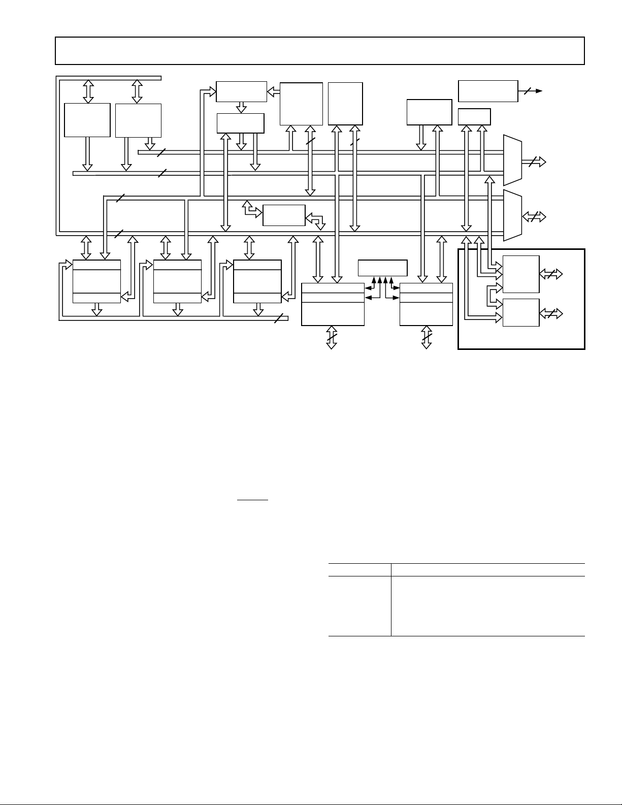
SYSTEM INTERFACE
Figure 3 shows a typical system for the ADSP-2101, ADSP2115, or ADSP-2103, with two serial I/O devices, a boot
EPROM, and optional external program and data memory. A
total of 15K words of data memory and 16K words of program
memory is addressable for the ADSP-2101 and ADSP-2103. A
total of 14.5K words of data memory and 15K words of
program memory is addressable for the ADSP-2115.
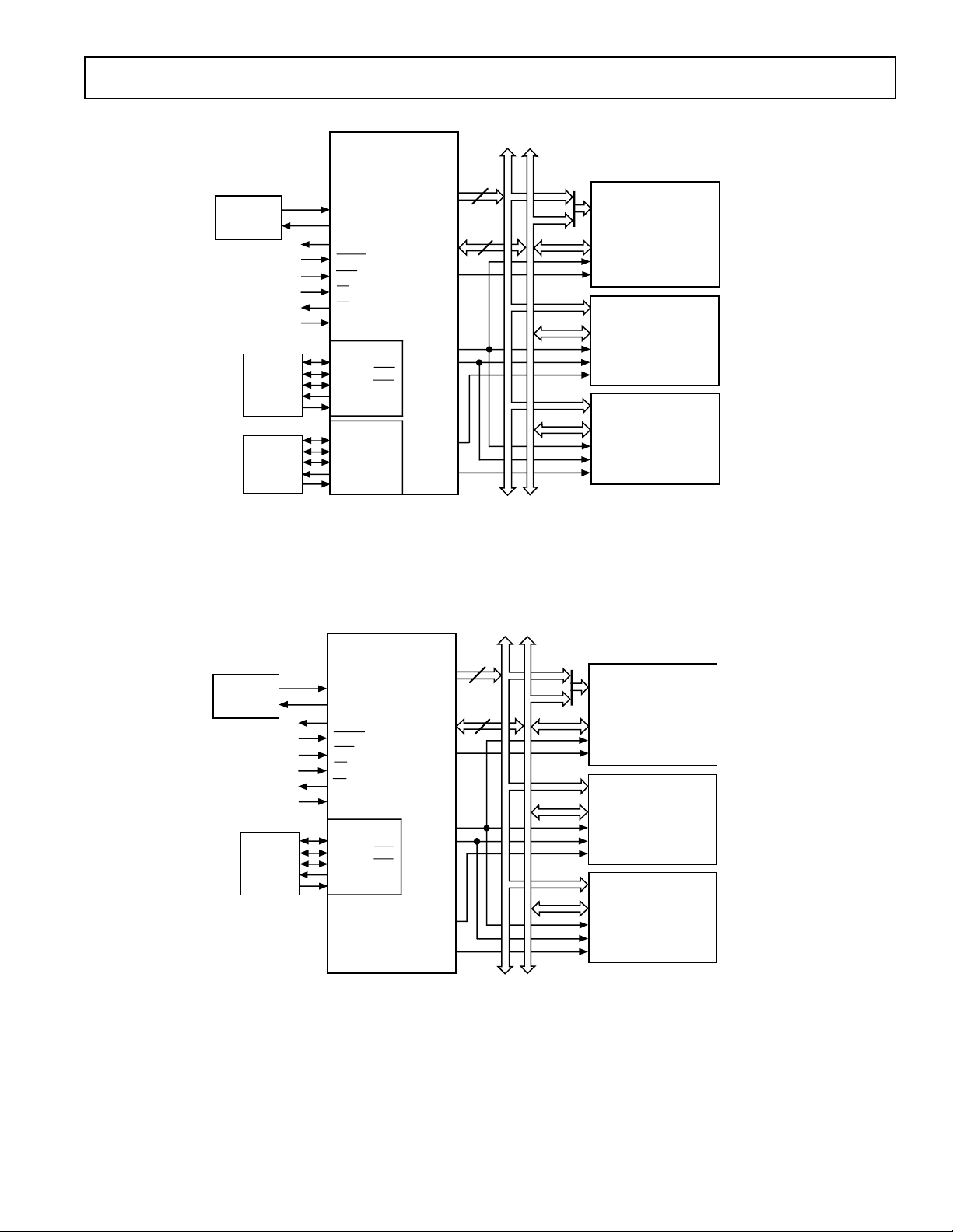
Figure 4 shows a system diagram for the ADSP-2105, with one
serial I/O device, a boot EPROM, and optional external
program and data memory. A total of 14.5K words of data
memory and 15K words of program memory is addressable for
the ADSP-2105.
Figure 5 shows a system diagram for the ADSP-2111, with two
serial I/O devices, a host processor, a boot EPROM, and
optional external program and data memory. A total of 15K
words of data memory and 16K words of program memory is
addressable.
Programmable wait-state generation allows the processors to
easily interface to slow external memories.
The ADSP-2101, ADSP-2103, ADSP-2115, and ADSP-2111
processors also provide either: one external interrupt (
IRQ2)
and two serial ports (SPORT0, SPORT1), or three external
interrupts (
The ADSP-2105 provides either: one external interrupt (
IRQ2, IRQ1, IRQ0) and one serial port (SPORT0).
IRQ2)
and one serial port (SPORT1), or three external interrupts
(
IRQ2, IRQ1, IRQ0) with no serial port.
Clock Signals
The ADSP-21xx processors’ CLKIN input may be driven by a
crystal or by a TTL-compatible external clock signal. The
CLKIN input may not be halted or changed in frequency during
operation, nor operated below the specified low frequency limit.
If an external clock is used, it should be a TTL-compatible
signal running at the instruction rate. The signal should be
connected to the processor’s CLKIN input; in this case, the
XTAL input must be left unconnected.
Because the ADSP-21xx processors include an on-chip oscillator circuit, an external crystal may also be used. The crystal
should be connected across the CLKIN and XTAL pins, with
two capacitors connected as shown in Figure 2. A parallelresonant, fundamental frequency, microprocessor-grade crystal
should be used.
CLKIN CLKOUT
ADSP-21xx
XTAL
REV. B
Figure 2. External Crystal Connections
–7–

ADSP-21xx
A clock output signal (CLKOUT) is generated by the processor,
synchronized to the processor’s internal cycles.
Reset
The RESET signal initiates a complete reset of the ADSP-21xx.
The
RESET signal must be asserted when the chip is powered
up to assure proper initialization. If the
RESET signal is applied
during initial power-up, it must be held long enough to allow
the processor’s internal clock to stabilize. If
RESET is activated
at any time after power-up and the input clock frequency does
not change, the processor’s internal clock continues and does
not require this stabilization time.
The power-up sequence is defined as the total time required for
the crystal oscillator circuit to stabilize after a valid V
DD
is
applied to the processor and for the internal phase-locked loop
(PLL) to lock onto the specific crystal frequency. A minimum of
2000 t
cycles will ensure that the PLL has locked (this does
CK
not, however, include the crystal oscillator start-up time).
During this power-up sequence the
held low. On any subsequent resets, the
meet the minimum pulse width specification, t
To generate the
RESET signal, use either an RC circuit with an
RESET signal should be
RESET signal must
.
RSP
external Schmidt trigger or a commercially available reset IC.
(Do not use only an RC circuit.)
Table IV. ADSP-21xx Pin Definitions
Pin # of Input /
Name(s) Pins Output Function
Address 14 O Address outputs for program, data and boot memory.
1
Data
24 I/O Data I/O pins for program and data memories. Input only for
boot memory, with two MSBs used for boot memory addresses.
Unused data lines may be left floating.
RESET 1 I Processor Reset Input
IRQ2 1 I External Interrupt Request #2
2
BR
1 I External Bus Request Input
BG 1 O External Bus Grant Output
PMS 1 O External Program Memory Select
DMS 1 O External Data Memory Select
BMS 1 O Boot Memory Select
RD 1 O External Memory Read Enable
WR 1 O External Memory Write Enable
MMAP 1 I Memory Map Select Input
CLKIN, XTAL 2 I External Clock or Quartz Crystal Input
CLKOUT 1 O Processor Clock Output
V
DD
GND Ground Pins
SPORT0
3
5 I/O Serial Port 0 Pins (TFS0, RFS0, DT0, DR0, SCLK0)
Power Supply Pins
SPORT1 5 I/O Serial Port 1 Pins (TFS1, RFS1, DT1, DR1, SCLK1)
or Interrupts & Flags:
IRQ0 (RFS1) 1 I External Interrupt Request #0
IRQ1 (TFS1) 1 I External Interrupt Request #1
FI (DR1) 1 I Flag Input Pin
FO (DT1) 1 O Flag Output Pin
FL2–0 (ADSP-2111 Only) 3 O General Purpose Flag Output Pins
Host Interface Port
(ADSP-2111 Only)
HSEL 1 I HIP Select Input
HACK 1 O HIP Acknowledge Output
HSIZE 1 I 8/16-Bit Host Select (0 = 16-Bit, 1 = 8-Bit)
BMODE 1 I Boot Mode Select (0 = Standard EPROM Booting, 1 = HIP Booting)
HMD0 1 I Bus Strobe Select (0 =
RD/WR, 1 = RW/DS)
HMD1 1 I HIP Address/Data Mode Select (0 = Separate, 1 = Multiplexed)
HRD/HRW 1 I HIP Read Strobe or Read/Write Select
HWR/HDS 1 I HIP Write Strobe or Host Data Strobe Select
HD15–0/HAD15-0 16 I/O HIP Data or HIP Data and Address
HA2/ALE 1 I Host Address 2 Input or Address Latch Enable Input
HA1–0/Unused 2 I Host Address 1 and 0 Inputs
NOTES
1
Unused data bus lines may be left floating.
2
BR must be tied high (to VDD) if not used.
3
ADSP-2105 does not have SPORT0. (SPORT0 pins are No Connects on the ADSP-2105.)
–8–
REV. B
1x CLOCK
or
CRYSTAL
SERIAL
DEVICE
(OPTIONAL)
SERIAL
DEVICE
(OPTIONAL)
ADSP-2101
or
ADSP-2103
or
ADSP-2115
CLKIN
XTAL
CLKOUT
RESET
IRQ2
BR
BG
MMAP
SPORT 1
SCLK1
RFS1 or IRQ0
TFS1 or IRQ1
DT1 or FO
DR1 or FI
SPORT 0
SCLK0
RFS0
TFS0
DT0
DR0
ADDR
DATA
13-0
23-0
BMS
WR
PMS
DMS
RD
ADSP-21xx
D
A
23-22
13-0
ADDR
D
15-8
DATA
OE
CS
A
13-0
ADDR
D
23-0
DATA
OE
WE
CS
A
13-0
ADDR
D
23-8
DATA
OE
WE
CS
BOOT
MEMORY
e.g. EPROM
2764
27128
27256
27512
PROGRAM
MEMORY
(OPTIONAL)
DATA
MEMORY
&
PERIPHERALS
(OPTIONAL)
14
24
THE TWO MSBs OF THE DATA BUS (D
BOOT MEMORY EPROM ADDRESS. THIS IS ONLY REQUIRED FOR THE 27256 AND 27512.
) ARE USED TO SUPPLY THE TWO MSBs OF THE
23-22
Figure 3. ADSP-2101/ADSP-2103/ADSP-2115 System
1x CLOCK
or
CRYSTAL
SERIAL
DEVICE
(OPTIONAL)
ADSP-2105
CLKIN
XTAL
CLKOUT
RESET
IRQ2
BR
BG
MMAP
SPORT 1
SCLK1
or
RFS1
TFS1
or
or
FO
DT1
or
FI
DR1
IRQ0
IRQ1
ADDR
DATA
14
13-0
24
23-0
BMS
RD
WR
PMS
DMS
D
A
23-22
13-0
D
15-8
A
13-0
D
23-0
A
13-0
D
23-8
ADDR
DATA
OE
CS
ADDR
DATA
OE
WE
CS
ADDR
DATA
OE
WE
CS
BOOT
MEMORY
e.g. EPROM
2764
27128
27256
27512
PROGRAM
MEMORY
(OPTIONAL)
DATA
MEMORY
&
PERIPHERALS
(OPTIONAL)
REV. B
THE TWO MSBs OF THE DATA BUS (D
BOOT MEMORY EPROM ADDRESS. THIS IS ONLY REQUIRED FOR THE 27256 AND 27512.
) ARE USED TO SUPPLY THE TWO MSBs OF THE
23-22
Figure 4. ADSP-2105 System
–9–
ADSP-21xx
1x CLOCK
or
CRYSTAL
SERIAL
DEVICE
(OPTIONAL)
SERIAL
DEVICE
(OPTIONAL)
ADSP-2111
IRQ0
IRQ1
FO
FI
ADDR
DATA
CONTROL
DATA / ADDR
CLKIN
XTAL
CLKOUT
RESET
IRQ2
BR
BG
MMAP
SPORT 1
SCLK1
RFS1
or
TFS1
or
DT1
or
DR1
or
SPORT 0
SCLK0
RFS0
TFS0
DT0
DR0
FL0
FL1
FL2
HOST INTERFACE PORT
13-0
23-0
BMS
RD
WR
PMS
DMS
14
24
7
16
A
13-0
D
23-22
D
15-8
A
13-0
D
23-0
A
13-0
D
23-8
HOST
PROCESSOR
(OPTIONAL)
ADDR
DATA
OE
CS
ADDR
DATA
OE
WE
CS
ADDR
DATA
OE
WE
CS
BOOT
MEMORY
(OPTIONAL)
e.g. EPROM
2764
27128
27256
27512
PROGRAM
MEMORY
(OPTIONAL)
DATA
MEMORY
&
PERIPHERALS
(OPTIONAL)
THE TWO MSBs OF THE DATA BUS (D
BOOT MEMORY EPROM ADDRESS. THIS IS ONLY REQUIRED FOR THE 27256 AND 27512.
) ARE USED TO SUPPLY THE TWO MSBs OF THE
23-22
Figure 5. ADSP-2111 System
The RESET input resets all internal stack pointers to the empty
stack condition, masks all interrupts, and clears the MSTAT
register. When
RESET is released, the boot loading sequence is
performed (provided there is no pending bus request and the
chip is configured for booting, with MMAP = 0). The first
instruction is then fetched from internal program memory
location 0x0000.
Program Memory Interface
The on-chip program memory address bus (PMA) and on-chip
program memory data bus (PMD) are multiplexed with the onchip data memory buses (DMA, DMD), creating a single
external data bus and a single external address bus. The external
data bus is bidirectional and is 24 bits wide to allow instruction
fetches from external program memory. Program memory may
contain code and data.
The external address bus is 14 bits wide. For the ADSP-2101,
ADSP-2103, and ADSP-2111, these lines can directly address
up to 16K words, of which 2K are on-chip. For the ADSP-2105
and ADSP-2115, the address lines can directly address up to
15K words, of which 1K is on-chip.
The data lines are bidirectional. The program memory select
(
PMS) signal indicates accesses to program memory and can be
used as a chip select signal. The write (
write operation and is used as a write strobe. The read (
WR) signal indicates a
RD)
signal indicates a read operation and is used as a read strobe or
output enable signal.
The ADSP-21xx processors write data from their 16-bit
registers to 24-bit program memory using the PX register to
provide the lower eight bits. When the processor reads 16-bit
data from 24-bit program memory to a 16-bit data register, the
lower eight bits are placed in the PX register.
The program memory interface can generate 0 to 7 wait states
for external memory devices; default is to 7 wait states after
RESET.
Program Memory Maps
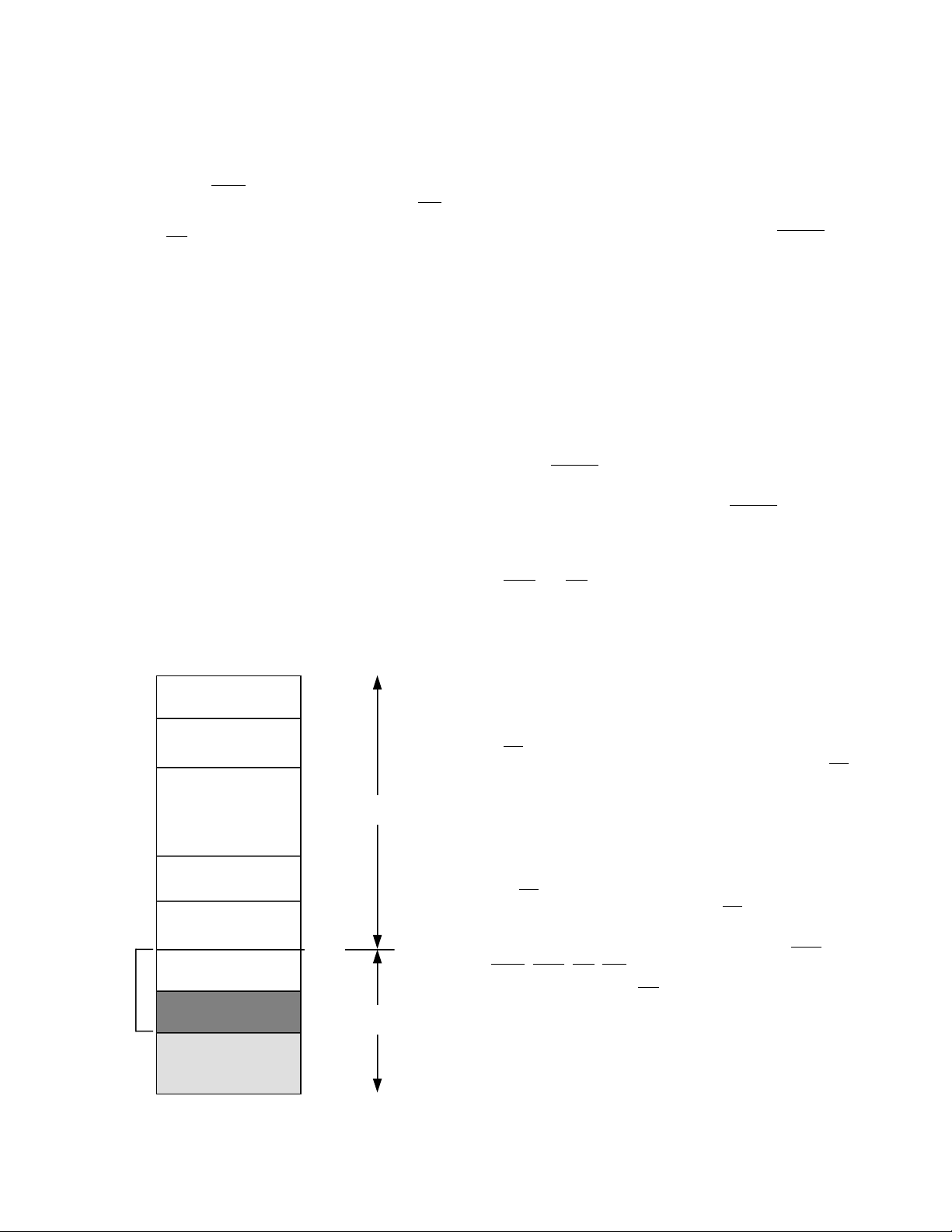
Program memory can be mapped in two ways, depending on the
state of the MMAP pin. Figure 6 shows the two program
memory maps for the ADSP-2101, ADSP-2103, and
ADSP-2111. Figure 8 shows the program memory maps for the
ADSP-2105 and ADSP-2115. Figures 7 and 9 show the
program memory maps for the ADSP-2161/62 and ADSP-2163/
64, respectively.
–10–
REV. B
ADSP-21xx
INTERNAL RAM
LOADED FROM
EXTERNAL
BOOT MEMORY
EXTERNAL
0x03FF
0x0400
0x3FFF
0x0000
EXTERNAL
0x3BFF
0x3C00
0x3FFF
0x0000
MMAP=0
MMAP=1
No Booting
0x37FF
0x3800
0x07FF
0x0800
RESERVED
1K
14K
14K
1K
INTERNAL RAM
1K
1K
RESERVED
4K
INTERNAL
ROM
12K
EXTERNAL
0x3FFF
0x0000
2K
EXTERNAL
0x3FFF
0x0000
MMAP=0 MMAP=1
0x37FF
0x3800
2K
INTERNAL
ROM
2K
INTERNAL
ROM
10K
EXTERNAL
0x07FF
0x0800
0x0FF0
0x0FFF
0x1000
0x0FF0
RESERVED
RESERVED
0x0FFF
0x1000
ADSP-2101/ADSP-2103/ADSP-2111
When MMAP = 0, on-chip program memory RAM occupies
2K words beginning at address 0x0000. Off-chip program
memory uses the remaining 14K words beginning at address
0x0800. In this configuration–when MMAP = 0–the boot
loading sequence (described below in “Boot Memory Interface”) is automatically initiated when
RESET is released.
When MMAP = 1, 14K words of off-chip program memory
begin at address 0x0000 and on-chip program memory RAM is
located in the upper 2K words, beginning at address 0x3800. In
this configuration, program memory is not booted although it
can be written to and read under program control.
INTERNAL
RAM
2K
LOADED FROM
EXTERNAL
BOOT MEMORY
EXTERNAL
14K
0x0000
0x07FF
0x0800
EXTERNAL
14K
0x0000
0x37FF
0x3800
ADSP-2105/ADSP-2115
When MMAP = 0, on-chip program memory RAM occupies
1K words beginning at address 0x0000. Off-chip program
memory uses the remaining 14K words beginning at address
0x0800. In this configuration–when MMAP = 0–the boot
loading sequence (described below in “Boot Memory Interface”) is automatically initiated when
RESET is released.
When MMAP = 1, 14K words of off-chip program memory
begin at address 0x0000 and on-chip program memory RAM is
located in the 1K words between addresses 0x3800–0x3BFF. In
this configuration, program memory is not booted although it
can be written to and read under program control.
MMAP=0 MMAP=1
Figure 6. ADSP-2101/ADSP-2103/ADSP-2111 Program
Memory Maps
8K
INTERNAL
ROM
RESERVED
Figure 7. ADSP-2161/62 Program Memory Maps
REV. B
8K
EXTERNAL
MMAP=0
0x3FFF
0x0000
0x1FF0
0x1FFF
0x2000
0x3FFF
INTERNAL
RAM
2K
No Booting
2K
EXTERNAL
6K
INTERNAL
ROM
RESERVED
6K
EXTERNAL
2K
INTERNAL
ROM
MMAP=1
0x3FFF
0x0000
0x07FF
0x0800
0x1FF0
0x1FFF
0x2000
0x37FF
0x3800
0x3FFF
Figure 8. ADSP-2105/ADSP-2115 Program Memory Maps
Figure 9. ADSP-2163/64 Program Memory Maps
–11–
ADSP-21xx
Data Memory Interface
The data memory address bus (DMA) is 14 bits wide. The
bidirectional external data bus is 24 bits wide, with the upper 16
bits used for data memory data (DMD) transfers.
The data memory select (
memory and can be used as a chip select signal. The write (
DMS) signal indicates access to data
WR)
signal indicates a write operation and can be used as a write
strobe. The read (
RD) signal indicates a read operation and can
be used as a read strobe or output enable signal.
The ADSP-21xx processors support memory-mapped I/O, with
the peripherals memory-mapped into the data memory address
space and accessed by the processor in the same manner as data
memory.
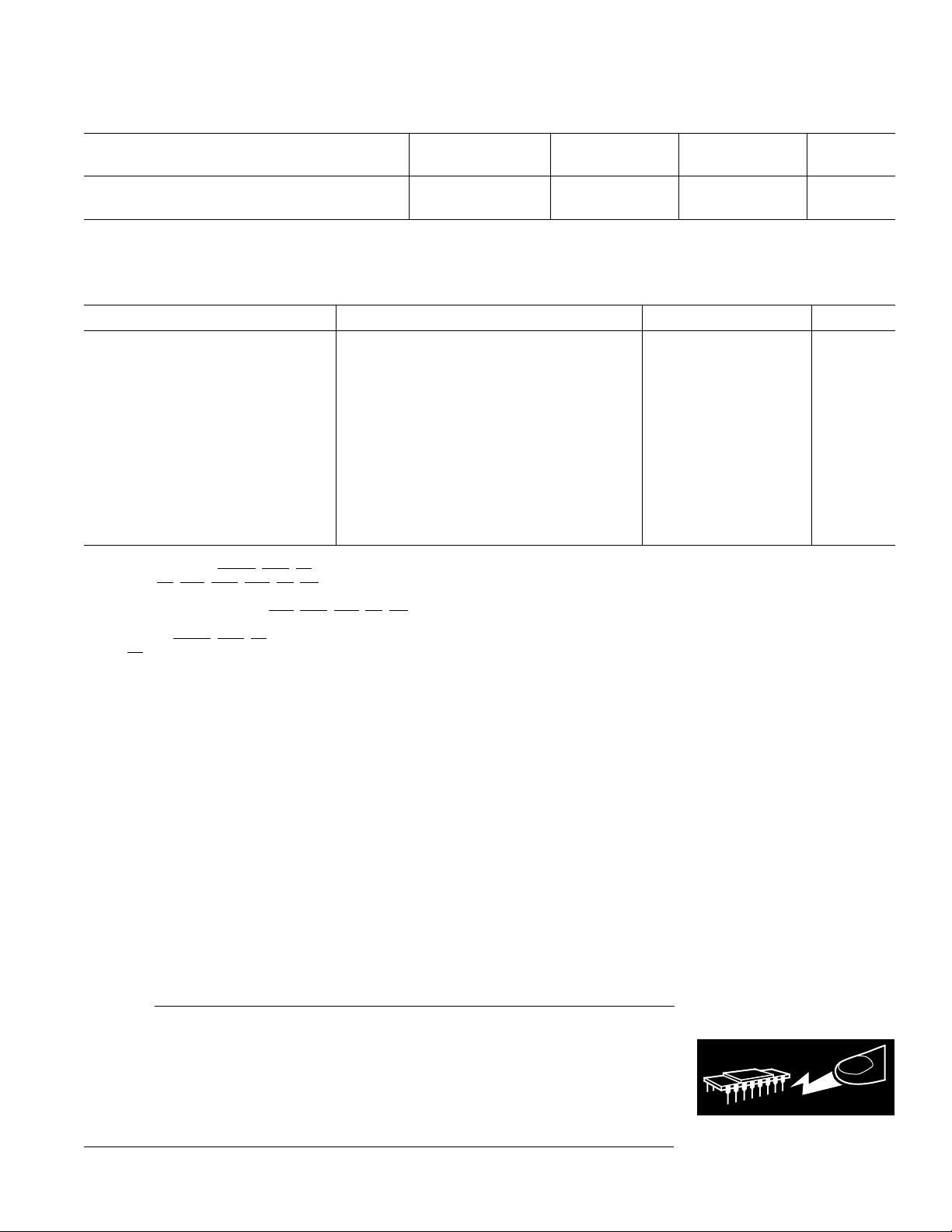
Data Memory Map
ADSP-2101/ADSP-2103/ADSP-2111
For the ADSP-2101, ADSP-2103, and ADSP-2111, on-chip
data memory RAM resides in the 1K words beginning at
address 0x3800, as shown in Figure 10. Data memory locations
from 0x3C00 to the end of data memory at 0x3FFF are
reserved. Control and status registers for the system, timer,
wait-state configuration, and serial port operations are located in
this region of memory.
ADSP-2105/ADSP-2115
For the ADSP-2105 and ADSP-2115, on-chip data memory
RAM resides in the 512 words beginning at address 0x3800,
also shown in Figure 10. Data memory locations from 0x3A00
to the end of data memory at 0x3FFF are reserved. Control and
status registers for the system, timer, wait-state configuration,
and serial port operations are located in this region of memory.
0x0000
1K EXTERNAL
1K for ADSP-2101
ADSP-2103
ADSP-2111
DWAIT0
1K EXTERNAL
DWAIT1
10K EXTERNAL
DWAIT2
1K EXTERNAL
DWAIT3
1K EXTERNAL
DWAIT4
512 for ADSP-2105
ADSP-2115
ADSP-216x
MEMORY-MAPPED
CONTROL REGISTERS
& RESERVED
0x0400
0x0800
0x3000
0x3400
0x3800
0x3A00
0x3C00
0x3FFF
EXTERNAL
RAM
INTERNAL
RAM
All Processors
The remaining 14K of data memory is located off-chip. This
external data memory is divided into five zones, each associated
with its own wait-state generator. This allows slower peripherals
to be memory-mapped into data memory for which wait states
are specified. By mapping peripherals into different zones, you
can accommodate peripherals with different wait-state requirements. All zones default to seven wait states after
RESET.
Boot Memory Interface
On the ADSP-2101, ADSP-2103, and ADSP-2111, boot
memory is an external 64K by 8 space, divided into eight
separate 8K by 8 pages. On the ADSP-2105 and ADSP-2115,
boot memory is a 32K by 8 space, divided into eight separate
4K by 8 pages. The 8-bit bytes are automatically packed into
24-bit instruction words by each processor, for loading into onchip program memory.
Three bits in the processors’ System Control Register select
which page is loaded by the boot memory interface. Another bit
in the System Control Register allows the forcing of a boot
loading sequence under software control. Boot loading from
Page 0 after
RESET is initiated automatically if MMAP = 0.
The boot memory interface can generate zero to seven wait
states; it defaults to three wait states after
RESET. This allows
the ADSP-21xx to boot from a single low cost EPROM such as
a 27C256. Program memory is booted one byte at a time and
converted to 24-bit program memory words.
The
BMS and RD signals are used to select and to strobe the
boot memory interface. Only 8-bit data is read over the data
bus, on pins D8-D15. To accommodate up to eight pages of
boot memory, the two MSBs of the data bus are used in the
boot memory interface as the two MSBs of the boot memory
address: D23, D22, and A13 supply the boot page number.
The ADSP-2100 Family Assembler and Linker allow the
creation of programs and data structures requiring multiple boot
pages during execution.
The
BR signal is recognized during the booting sequence. The
bus is granted after loading the current byte is completed.
BR
during booting may be used to implement booting under control
of a host processor.
Bus Interface
The ADSP-21xx processors can relinquish control of their data
and address buses to an external device. When the external
device requires control of the buses, it asserts the bus request
signal (
BR). If the ADSP-21xx is not performing an external
memory access, it responds to the active
BR input in the next
cycle by:
•
Three-stating the data and address buses and the PMS,
DMS, BMS, RD, WR output drivers,
•
Asserting the bus grant (BG) signal,
•
and halting program execution.
If the Go mode is set, however, the ADSP-21xx will not halt
program execution until it encounters an instruction that
requires an external memory access.
Figure 10. Data Memory Map (All Processors)
–12–
REV. B

ADSP-21xx
If the ADSP-21xx is performing an external memory access
when the external device asserts the
state the memory interfaces or assert the
cycle after the access completes (up to eight cycles later depending on the number of wait states). The instruction does not need
to be completed when the bus is granted; the ADSP-21xx will
grant the bus in between two memory accesses if an instruction
requires more than one external memory access.
When the
signal, re-enables the output drivers and continues program
execution from the point where it stopped.
The bus request feature operates at all times, including when
the processor is booting and when
feature is not used, the
Low Power IDLE Instruction
The IDLE instruction places the ADSP-21xx processor in low
power state in which it waits for an interrupt. When an interrupt
occurs, it is serviced and execution continues with instruction
following IDLE. Typically this next instruction will be a JUMP
back to the IDLE instruction. This implements a low-power
standby loop.
The IDLE n instruction is a special version of IDLE that slows
the processor’s internal clock signal to further reduce power
consumption. The reduced clock frequency, a programmable
fraction of the normal clock rate, is specified by a selectable
divisor, n, given in the IDLE instruction. The syntax of the
instruction is:
where n = 16, 32, 64, or 128.
The instruction leaves the chip in an idle state, operating at the
slower rate. While it is in this state, the processor’s other
internal clock signals, such as SCLK, CLKOUT, and the timer
clock, are reduced by the same ratio. Upon receipt of an
enabled interrupt, the processor will stay in the IDLE state for
up to a maximum of n CLKIN cycles, where n is the divisor
specified in the instruction, before resuming normal operation.
When the IDLE n instruction is used, it slows the processor’s
internal clock and thus its response time to incoming interrupts–
the 1-cycle response time of the standard IDLE state is increased by n, the clock divisor. When an enabled interrupt is
received, the ADSP-21xx will remain in the IDLE state for up
to a maximum of n CLKIN cycles (where n = 16, 32, 64, or
128) before resuming normal operation.
When the IDLE n instruction is used in systems that have an
externally generated serial clock (SCLK), the serial clock rate
may be faster than the processor’s reduced internal clock rate.
Under these conditions, interrupts must not be generated at a
faster rate than can be serviced, due to the additional time the
processor takes to come out of the IDLE state (a maximum of n
CLKIN cycles).
ADSP-216x Prototyping
You can prototype your ADSP-216x system with either the
ADSP-2101 or ADSP-2103 RAM-based processors. When code
is fully developed and debugged, it can be submitted to Analog
BR signal is released, the processor releases the BG
BR input should be tied high (to VDD).
IDLE n;
BR signal, it will not three-
BG signal until the
RESET is active. If this
Devices for conversion into a ADSP-216x ROM product.
The ADSP-2101 EZ-ICE emulator can be used for develop-
ment of ADSP-216x systems. For the 3.3 V ADSP-2162 and
ADSP-2164, a voltage converter interface board provides 3.3 V
emulation.
Additional overlay memory is used for emulation of ADSP-
2161/62 systems. It should be noted that due to the use of off-
chip overlay memory to emulate the ADSP-2161/62, a perfor-
mance loss may be experienced when both executing instruc-
tions and fetching program memory data from the off-chip
overlay memory in the same cycle. This can be overcome by
locating program memory data in on-chip memory.
Ordering Procedure for ADSP-216x ROM Processors
To place an order for a custom ROM-coded ADSP-2161,
ADSP-2162, ADSP-2163, or ADSP-2164 processor, you must:
1. Complete the following forms contained in the ADSP ROM
Ordering Package, available from your Analog Devices sales
representative:
ADSP-216x ROM Specification Form
ROM Release Agreement
ROM NRE Agreement & Minimum Quantity Order (MQO)
Acceptance Agreement for Pre-Production ROM Products
2. Return the forms to Analog Devices along with two copies of
the Memory Image File (.EXE file) of your ROM code. The
files must be supplied on two 3.5" or 5.25" floppy disks for
the IBM PC (DOS 2.01 or higher).
3. Place a purchase order with Analog Devices for non-recurring
engineering changes (NRE) associated with ROM product
development.
After this information is received, it is entered into Analog
Devices’ ROM Manager System which assigns a custom ROM
model number to the product. This model number will be
branded on all prototype and production units manufactured to
these specifications.
To minimize the risk of code being altered during this process,
Analog Devices verifies that the .EXE files on both floppy disks
are identical, and recalculates the checksums for the .EXE file
entered into the ROM Manager System. The checksum data, in
the form of a ROM Memory Map, a hard copy of the .EXE file,
and a ROM Data Verification form are returned to you for
inspection.
REV. B
–13–

ADSP-21xx
A signed ROM Verification Form and a purchase order for
production units are required prior to any product being
manufactured. Prototype units may be applied toward the
minimum order quantity.
Upon completion of prototype manufacture, Analog Devices
will ship prototype units and a delivery schedule update for
production units. An invoice against your purchase order for the
NRE charges is issued at this time.
There is a charge for each ROM mask generated and a minimum order quantity. Consult your sales representative for
details. A separate order must be placed for parts of a specific
package type, temperature range, and speed grade.
Functional Differences for Older Revision Devices
Older revisions of the ADSP-21xx processors have slight
differences in functionality. The two differences are as follows:
•
Bus Grant (BG) is asserted in the same cycle that Bus
Request (
requirements are met for the
a synchronous input rather than asynchronous. (In newer
revision devices,
recognized.)
•
Only the standard IDLE instruction is available, not the
clock-reducing IDLE n instruction.
To determine the revision of a particular ADSP-21xx device,
inspect the marking on the device. For example, an ADSP-2101
of revision 6.0 will have the following marking:
BR) is recognized (i.e. when setup and hold time
BR input). Bus Request input is
BG is asserted in the cycle after BR is
a
ADSP-2101
KS-66
EE/A12345-6.0
∆
9234
The revision codes for the older versions of each ADSP-21xx
device are as follows:
Package & Speed
←
Lot # & Revision Code
←
←
Date Code
Processor Old Functionality New Functionality
ADSP-2101 Revision Code ≤ 5.0 Revision Code ≥ 6.0
ADSP-2105 No Revision Code Revision Code ≥ 1.0
ADSP-2115 Revision Code < 1.0 Revision Code ≥ 1.0
ADSP-2111 RevisionCode < 2.0 Revision Code ≥ 2.0
ADSP-2103 Revision code ≤ 5.0 Revision code ≥ 6.0
–14–
REV. B

ADSP-21xx
Instruction Set
The ADSP-21xx assembly language uses an algebraic syntax for
ease of coding and readability. The sources and destinations of
computations and data movements are written explicitly in each
assembly statement, eliminating cryptic assembler mnemonics.
Every instruction assembles into a single 24-bit word and
executes in a single cycle. The instructions encompass a wide
variety of instruction types along with a high degree of
operational parallelism. There are five basic categories of
instructions: data move instructions, computational instructions, multifunction instructions, program flow control instructions and miscellaneous instructions. Multifunction instructions
perform one or two data moves and a computation.
The instruction set is summarized below. The ADSP-2100
Family Users Manual contains a complete reference to the
instruction set.
ALU Instructions
[IF cond] AR|AF = xop + yop [+ C] ; Add/Add with Carry
= xop – yop [+ C– 1] ; Subtract X – Y/Subtract X – Y with Borrow
= yop – xop [+ C– 1] ; Subtract Y – X/Subtract Y – X with Borrow
= xop AND yop ; AND
= xop OR yop ; OR
= xop XOR yop ; XOR
= PASS xop ; Pass, Clear
= – xop ; Negate
= NOT xop ; NOT
= ABS xop ; Absolute Value
= yop + 1 ; Increment
= yop – 1 ; Decrement
= DIVS yop, xop ; Divide
= DIVQ xop ;
MAC Instructions
[IF cond] MR|MF = xop * yop ; Multiply
= MR + xop * yop ; Multiply/Accumulate
= MR – xop * yop ; Multiply/Subtract
= MR ; Transfer MR
IF MV SAT MR ; Conditional MR Saturation
=0 ; Clear
Shifter Instructions
[IF cond] SR = [SR OR] ASHIFT xop ; Arithmetic Shift
[IF cond] SR = [SR OR] LSHIFT xop ; Logical Shift
SR = [SR OR] ASHIFT xop BY <exp>; Arithmetic Shift Immediate
[IF cond] SE = EXP xop ; Derive Exponent
[IF cond] SB = EXPADJ xop ; Block Exponent Adjust
[IF cond] SR = [SR OR] NORM xop ; Normalize
SR = [SR OR] LSHIFT xop BY <exp>; Logical Shift Immediate
Data Move Instructions
reg = reg ; Register-to-Register Move
reg = <data> ; Load Register Immediate
reg = DM (<addr>) ; Data Memory Read (Direct Address)
dreg = DM (Ix , My) ; Data Memory Read (Indirect Address)
dreg = PM (Ix , My) ; Program Memory Read (Indirect Address)
DM (<addr>) = reg ; Data Memory Write (Direct Address)
DM (Ix , My) = dreg ; Data Memory Write (Indirect Address)
PM (Ix , My) = dreg ; Program Memory Write (Indirect Address)
Multifunction Instructions
<ALU>|<MAC>|<SHIFT> , dreg = dreg ; Computation with Register-to-Register Move
<ALU>|<MAC>|<SHIFT> , dreg = DM (Ix , My) ; Computation with Memory Read
<ALU>|<MAC>|<SHIFT> , dreg = PM (Ix , My) ; Computation with Memory Read
DM (Ix , My) = dreg , <ALU>|<MAC>|<SHIFT> ; Computation with Memory Write
PM (Ix , My) = dreg , <ALU>|<MAC>|<SHIFT> ; Computation with Memory Write
dreg = DM (Ix , My) , dreg = PM (Ix , My) ; Data & Program Memory Read
<ALU>|<MAC> , dreg = DM (Ix , My) , dreg = PM (Ix , My) ; ALU/MAC with Data & Program Memory Read
REV. B
–15–

ADSP-21xx
Program Flow Instructions
DO <addr> [UNTIL term] ; Do Until Loop
[IF cond] JUMP (Ix) ; Jump
[IF cond] JUMP <addr>;
[IF cond] CALL (Ix) ; Call Subroutine
[IF cond] CALL <addr>;
IF [NOT ] FLAG_IN JUMP <addr>; Jump/Call on Flag In Pin
IF [NOT ] FLAG_IN CALL <addr>;
[IF cond] SET|RESET|TOGGLE FLAG_OUT [, ...] ; Modify Flag Out Pin
[IF cond] RTS ; Return from Subroutine
[IF cond] RTI ; Return from Interrupt Service Routine
IDLE [(n)] ; Idle
Miscellaneous Instructions
NOP ; No Operation
MODIFY (Ix , My); Modify Address Register
[PUSH STS] [, POP CNTR] [, POP PC] [, POP LOOP] ; Stack Control
ENA|DIS SEC_REG [, ...] ; Mode Control
Notation Conventions
Ix Index registers for indirect addressing
My Modify registers for indirect addressing
<data> Immediate data value
<addr> Immediate address value
<exp> Exponent (shift value) in shift immediate instructions (8-bit signed number)
<ALU> Any ALU instruction (except divide)
<MAC> Any multiply-accumulate instruction
<SHIFT> Any shift instruction (except shift immediate)
cond Condition code for conditional instruction
term Termination code for DO UNTIL loop
dreg Data register (of ALU, MAC, or Shifter)
reg Any register (including dregs)
; A semicolon terminates the instruction
, Commas separate multiple operations of a single instruction
[ ] Optional part of instruction
[, ...] Optional, multiple operations of an instruction
option1 | option2 List of options; choose one.
BIT_REV
AV_LATCH
AR_SAT
M_MODE
TIMER
G_MODE
Assembly Code Example
The following example is a code fragment that performs the filter tap update for an adaptive filter based on a least-mean-squared
algorithm. Notice that the computations in the instructions are written like algebraic equations.
MF=MX0*M Y1(RND), MX0=DM(I2,M1); { M F=error*beta}
MR=MX0*M F(RND), AY0=PM(I6,M5);
DO adapt UNTIL CE;
AR=MR1+AY0, MX0=DM(I2,M1), AY0=PM(I6,M7);
adapt: PM(I6,M6)= AR, MR=MX0*M F(RND);
MODIFY(I2,M3); {Point to oldest data}
MODIFY(I6,M7); {Point to start of data}
–16–
REV. B
ADSP-2101/2105/2115/2161/2163–SPECIFICATIONS
WARNING!
ESD SENSITIVE DEVICE
ADSP-21xx
RECOMMENDED OPERATING CONDITIONS
K Grade B Grade T Grade
Parameter Min Max Min Max Min Max Unit
V
DD
T
AMB
See “Environmental Conditions” for information on thermal specifications.
Supply Voltage 4.50 5.50 4.50 5.50 4.50 5.50 V
Ambient Operating Temperature 0 +70 –40 +85 –55 +125 °C
ELECTRICAL CHARACTERISTICS
Parameter Test Conditions Min Max Unit
V
V
V
V
V
I
I
I
I
C
C
NOTES
10
Specifications subject to change without notice.
Hi-Level Input Voltage
IH
Hi-Level CLKIN Voltage @ V
IH
Lo-Level Input Voltage
IL
Hi-Level Output Voltage
OH
Lo-Level Output Voltage
OL
Hi-Level Input Current
IH
Lo-Level Input Current
IL
Tristate Leakage Current
OZH
Tristate Leakage Current
OZL
Input Pin Capacitance
I
Output Pin Capacitance
O
1
Input-only pins: CLKIN, RESET, IRQ2, BR, MMAP, DR1, DR0 (not on ADSP-2105).
2
Output pins: BG, PMS, DMS, BMS, RD, WR, A0–A13, CLKOUT, DT1, DT0 (not on ADSP-2105).
3
Bidirectional pins: D0–D23, SCLK1, RFS1, TFS1, SCLK0 (not on ADSP-2105), RFS0 (not on ADSP-2105), TFS0 (not on ADSP-2105).
4
Tristatable pins: A0–A13, D0–D23, PMS, DMS, BMS, RD, WR, DT1, SCLK1, RSF1, TFS1, DT0 (not on ADSP-2105), SCLK0 (not on ADSP-2105),
RFS0 (not on ADSP-2105), TFS0 (not on ADSP-2105).
5
Input-only pins: RESET, IRQ2, BR, MMAP, DR1, DR0 (not on ADSP-2105).
6
0 V on BR, CLKIN Active (to force tristate condition).
7
Although specified for TTL outputs, all ADSP-21xx outputs are CMOS-compatible and will drive to VDD and GND, assuming no dc loads.
8
Guaranteed but not tested.
9
Applies to PGA, PLCC, PQFP package types.
Output pin capacitance is the capacitive load for any three-stated output pin.
3, 5
1, 3
2, 3, 7
2, 3, 7
1
1
4
4
1, 8, 9
4, 8, 9, 10
@ V
= max 2.0 V
DD
= max 2.2 V
DD
@ VDD = min 0.8 V
@ VDD = min, IOH = –0.5 mA 2.4 V
@ V
= min, IOH = –100 µA
DD
8
VDD – 0.3 V
@ VDD = min, IOL = 2 mA 0.4 V
@ VDD = max, VIN = VDD max 10 µA
@ VDD = max, VIN = 0 V 10 µA
@ VDD = max, VIN = VDD max
@ VDD = max, VIN = 0 V
@ VIN = 2.5 V, fIN = 1.0 MHz, T
@ VIN = 2.5 V, fIN = 1.0 MHz, T
6
6
= 25°C8pF
AMB
= 25°C8pF
AMB
10 µA
10 µA
ABSOLUTE MAXIMUM RATINGS
Supply Voltage . . . . . . . . . . . . . . . . . . . . . . . . . . –0.3 V to +7 V
Input Voltage . . . . . . . . . . . . . . . . . . . . . –0.3 V to V
Output Voltage Swing . . . . . . . . . . . . . . –0.3 V to V
Operating Temperature Range (Ambient) . . . –55ºC to +125ºC
Storage Temperature Range . . . . . . . . . . . . . –65ºC to +150ºC
Lead Temperature (10 sec) PGA . . . . . . . . . . . . . . . . . +300ºC
Lead Temperature (5 sec) PLCC, PQFP, TQFP . . . . +280ºC
*Stresses greater than those listed above may cause permanent damage to the
device. These are stress ratings only, and functional operation of the device at these
or any other conditions greater than those indicated in the operational sections of
this specification is not implied. Exposure to absolute maximum rating conditions
for extended periods may affect device reliability.
CAUTION
ESD (electrostatic discharge) sensitive device. Electrostatic charges as high as 4000 V readily
accumulate on the human body and test equipment and can discharge without detection. Although
the ADSP-21xx processors feature proprietary ESD protection circuitry to dissipate high energy
electrostatic discharges (Human Body Model), permanent damage may occur to devices subjected
to such discharges. Therefore, proper ESD precautions are recommended to avoid performance
degradation or loss of functionality. Unused devices must be stored in conductive foam or shunts,
and the foam should be discharged to the destination socket before the devices are removed. Per
method 3015 of MIL-STD-883, the ADSP-21xx processors have been classified as Class 1 devices.
REV. B
*
+ 0.3 V
DD
+ 0.3 V
DD
–17–
ADSP-21xx
SPECIFICATIONS (ADSP-2101/2105/2115/2161/2163)
SUPPLY CURRENT & POWER (ADSP-2101/2105/2115/2161/2163)
Parameter Test Conditions Min Max Unit
1, 3
1
@ VDD = max, tCK = 40 ns
@ V
= max, t
DD
@ V
= max, tCK = 72.3 ns
DD
CK
@ VDD = max, tCK = 40 ns
@ V
= max, tCK = 50 ns 11 mA
DD
I
I
Supply Current (Dynamic)
DD
Supply Current (Idle)
DD
@ VDD = max, tCK = 72.3 ns 10 mA
NOTES
1
Current reflects device operating with no output loads.
2
VIN = 0.4 V and 2.4 V.
3
Idle refers to ADSP-21xx state of operation during execution of IDLE instruction. Deasserted pins are driven to either VDD or GND.
4
ADSP-2105 is not available in a 25 MHz speed grade.
For typical supply current (internal power dissipation) figures, see Figure 11.
2
= 50 ns
4
2
2
38 mA
31 mA
24 mA
12 mA
70
60
51mW
50
40
38mW
30
POWER – mW
28mW
20
10
IDD IDLE
V
DD =
V
DD =
V
DD =
220
200
180
160
140
POWER – mW
120
100
80
60
1,2
5.5V
5.0V
4.5V
129mW
100mW
64mW
49mW
35mW
74mW
IDD DYNAMIC
V
5.5V
DD =
V
5.0V
DD =
V
4.5V
DD =
FREQUENCY – MHz
65
60
55
50
45
POWER – mW
40
35
1
205mW
157mW
118mW
51mW
41mW
40mW
30.0020.0013.8310.00 25.00
IDD IDLE n MODES
IDD IDLE
IDLE 16
IDLE 128
3
64mW
43mW
42mW
0
FREQUENCY – MHz
VALID FOR ALL TEMPERATURE GRADES.
1
POWER REFLECTS DEVICE OPERATING WITH NO OUTPUT LOADS.
2
IDLE REFERS TO ADSP-21xx OPERATION DURING EXECUTION OF IDLE INSTRUCTION.
DEASSERTED PINS ARE DRIVEN TO EITHER VDD OR GND.
3
MAXIMUM POWER DISSIPATION AT V
30.0020.0013.8310.00 25.00
DD =
30
FREQUENCY – MHz
5.5V DURING EXECUTION OF
IDLE n
30.0020.0013.8310.00 25.00
INSTRUCTION.
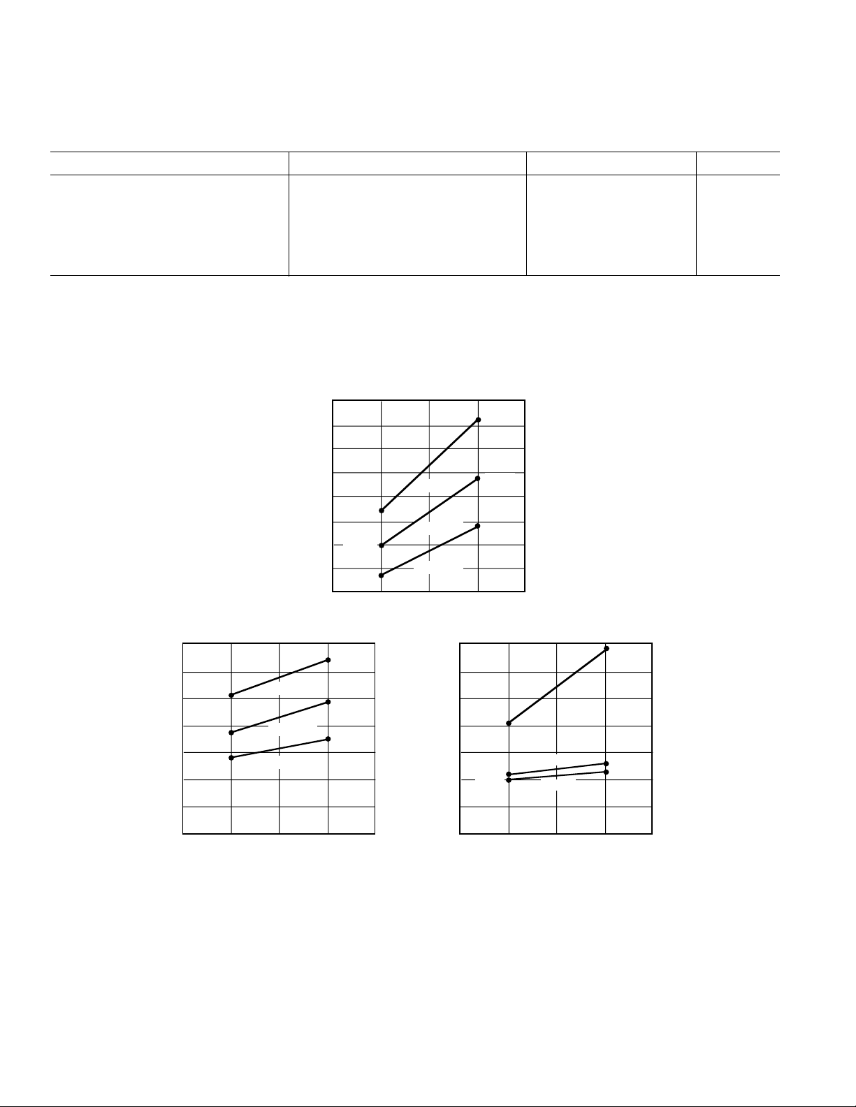
Figure 11. ADSP-2101 Power (Typical) vs. Frequency
–18–
REV. B
SPECIFICATIONS (ADSP-2101/2105/2115/2161/2163)
CL – pF
25 1501251007550
RISE TIME (0.8V - 2.0V) – ns
VDD = 4.5V
8
7
6
5
4
3
2
1
0
1750
POWER DISSIPATION EXAMPLE
To determine total power dissipation in a specific application,
the following equation should be applied for each output:
C × V
C = load capacitance, f = output switching frequency.
Example:
In an ADSP-2101 application where external data memory is
used and no other outputs are active, power dissipation is
calculated as follows:
Assumptions:
•
External data memory is accessed every cycle with 50% of the
address pins switching.
•
External data memory writes occur every other cycle with
50% of the data pins switching.
•
Each address and data pin has a 10 pF total load at the pin.
•
The application operates at V
Total Power Dissipation = P
= internal power dissipation (from Figure 11).
P
INT
(C × V
2
× f ) is calculated for each output:
DD
2
× f
DD
= 5.0 V and t
DD
+ (C × V
INT
= 50 ns.
CK
2
× f )
DD
ADSP-21xx
CAPACITIVE LOADING
Figures 12 and 13 show capacitive loading characteristics for the
ADSP-2101, ADSP-2105, ADSP-2115, and ADSP-2161/2163.
Figure 12. Typical Output Rise Time vs. Load Capacitance, C
(at Maximum Ambient Operating Temperature)
L
# of
Output Pins × C × V
DD
2
× f
Address, DMS 8 × 10 pF × 52 V × 20 MHz = 40.0 mW
Data,
WR 9 × 10 pF × 52 V × 10 MHz = 22.5 mW
RD 1 × 10 pF × 52 V × 10 MHz = 2.5 mW
CLKOUT 1 × 10 pF × 52 V × 20 MHz = 5.0 mW
5
4
3
2
1
VDD = 4.5V
70.0 mW
Total power dissipation for this example = P
INT
ENVIRONMENTAL CONDITIONS
Ambient Temperature Rating:
= T
T
AMB
T
= Case Temperature in °C
CASE
– (PD × θCA)
CASE
+ 70.0 mW.
0
–1
–2
VALID OUTPUT DELAY OR HOLD – ns
–3
25 100 12550 75 150
CL – pF
1750
PD = Power Dissipation in W
θ
= Thermal Resistance (Case-to-Ambient)
CA
θ
= Thermal Resistance (Junction-to-Ambient)
JA
θ
= Thermal Resistance (Junction-to-Case)
JC
Package θ
JA
θ
JC
θ
CA
Figure 13. Typical Output Valid Delay or Hold vs. Load
Capacitance, C
(at Maximum Ambient Operating Temperature)
L
PGA 18°C/W 9°C/W 9°C/W
PLCC 27°C/W 16°C/W 11°C/W
PQFP 60°C/W 18°C/W 42 °C/W
TQFP 60°C/W 18°C/W 42°C/W
REV. B
–19–
ADSP-21xx
SPECIFICATIONS (ADSP-2101/2105/2115/2161/2163)
TEST CONDITIONS
Figure 14 shows voltage reference levels for ac measurements.
INPUT
OUTPUT
Figure 14. Voltage Reference Levels for AC Measurements
(Except Output Enable/Disable)
Output Disable Time
Output pins are considered to be disabled when they have
stopped driving and started a transition from the measured
output high or low voltage to a high impedance state. The
output disable time (t
t
, as shown in Figure 15. The time t
DECAY
) is the difference of t
DIS
interval from when a reference signal reaches a high or low
voltage level to when the output voltages have changed by 0.5 V
from the measured output high or low voltage.
3.0V
1.5V
0.0V
2.0V
1.5V
0.8V
MEASURED
MEASURED
and
is the
The decay time, t
C
, and the current load, iL, on the output pin. It can be
L
, is dependent on the capacitative load,
DECAY
approximated by the following equation:
×0.5V
C
t
DECAY
L
=
i
L
from which
t
DIS
= t
MEASURED
– t
DECAY
is calculated. If multiple pins (such as the data bus) are disabled, the measurement value is that of the last pin to stop
driving.
Output Enable Time
Output pins are considered to be enabled when they have made
a transition from a high-impedance state to when they start
driving. The output enable time (t
) is the interval from
ENA
when a reference signal reaches a high or low voltage level to
when the output has reached a specified high or low trip point,
as shown in Figure 15. If multiple pins (such as the data bus)
are enabled, the measurement value is that of the first pin to
start driving.
REFERENCE
SIGNAL
VOH (MEASURED)
VOL (MEASURED)
OUTPUT
t
DECAY
OUTPUT STOPS
TO
OUTPUT
PIN
t
MEASURED
t
DIS
VOH (MEASURED) – 0.5V
VOL (MEASURED) +0.5V
DRIVING
HIGH-IMPEDANCE STATE.
TEST CONDITIONS CAUSE
THIS VOLTAGE LEVEL TO BE
APPROXIMATELY 1.5V.
Figure 15. Output Enable/Disable
I
OL
50pF
t
ENA
2.0V
1.0V
OUTPUT STARTS
DRIVING
+1.5V
VOH (MEASURED)
VOL (MEASURED)
I
OH
Figure 16. Equivalent Device Loading for AC Measurements
(Except Output Enable/Disable)
–20–
REV. B

ADSP-2111–SPECIFICA TIONS
ADSP-21xx
RECOMMENDED OPERATING CONDITIONS
K Grade B Grade T Grade
Parameter Min Max Min Max Min Max Unit
V
DD
T
AMB
See “Environmental Conditions” for information on thermal specifications.
Supply Voltage 4.50 5.50 4.50 5.50 4.50 5.50 V
Ambient Operating Temperature 0 +70 –40 +85 –55 +125 °C
ELECTRICAL CHARACTERISTICS
Parameter Test Conditions Min Max Unit
V
V
V
V
V
I
I
I
I
C
C
NOTES
10
Specifications subject to change without notice.
Hi-Level Input Voltage
IH
Hi-Level CLKIN Voltage @ V
IH
Lo-Level Input Voltage
IL
Hi-Level Output Voltage
OH
Lo-Level Output Voltage
OL
Hi-Level Input Current
IH
Lo-Level Input Current
IL
Tristate Leakage Curren
OZH
Tristate Leakage Current
OZL
Input Pin Capacitance
I
Output Pin Capacitance
O
1
Input-only pins: CLKIN, RESET, IRQ2, BR, MMAP, DR1, DR0, HSEL, HSIZE, BMODE, HMD0, HMD1, HRD/HRW, HWR/HDS, HA2/ALE, HA1-0.
2
Output pins: BG, PMS, DMS, BMS, RD, WR, A0–A13, CLKOUT, DT1, DT0, HACK, FL2-0.
3
Bidirectional pins: D0–D23, SCLK1, RFS1, TFS1, SCLK0, RFS0, TFS0, HD0–HD15/HAD0–HAD15.
4
Tristatable pins: A0–A13, D0–D23, PMS, DMS, BMS, RD, WR, DT1, SCLK1, RSF1, TFS1, DT0, SCLK0, RFS0, TFS0, HD0–HD15/HAD0–HAD15.
5
Input-only pins: RESET, IRQ2, BR, MMAP, DR1, DR0, HSEL, HSIZE, BMODE, HMD0, HMD1, HRD/HRW, HWR/HDS, HA2/ALE, HA1-0.
6
0 V on BR, CLKIN Active (to force tristate condition).
7
Although specified for TTL outputs, all ADSP-2111 outputs are CMOS-compatible and will drive to VDD and GND, assuming no dc loads.
8
Guaranteed but not tested.
9
Applies to ADSP-2111 PGA and PQFP packages.
Output pin capacitance is the capacitive load for any three-stated output pin.
3, 5
1, 3
2, 3, 7
2, 3, 7
1
1
4
4
1, 8, 9
4, 8, 9, 10
@ V
= max 2.0 V
DD
= max 2.2 V
DD
@ VDD = min 0.8 V
@ VDD = min, IOH = –0.5 mA 2.4 V
@ V
= min, IOH = –100 µA
DD
8
VDD – 0.3 V
@ VDD = min, IOL = 2 mA 0.4 V
@ VDD = max, VIN = VDD max 10 µA
@ VDD = max, VIN = 0V 10 µA
@ VDD = max, VIN = VDD max
@ VDD = max, VIN = 0V
@ VIN = 2.5 V, fIN = 1.0 MHz, T
@ VIN = 2.5 V, fIN = 1.0 MHz, T
6
6
= 25°C8pF
AMB
= 25°C8pF
AMB
10 µA
10 µA
ABSOLUTE MAXIMUM RATINGS*
Supply Voltage . . . . . . . . . . . . . . . . . . . . . . . . . . –0.3 V to +7 V
Input Voltage . . . . . . . . . . . . . . . . . . . . . –0.3 V to V
Output Voltage Swing . . . . . . . . . . . . . . –0.3 V to V
+ 0.3 V
DD
+ 0.3 V
DD
Operating Temperature Range (Ambient) . . . –55ºC to +125ºC
Storage Temperature Range . . . . . . . . . . . . . –65ºC to +150ºC
Lead Temperature (10 sec) PGA . . . . . . . . . . . . . . . . . +300ºC
Lead Temperature (5 sec) PQFP . . . . . . . . . . . . . . . . . +280ºC
*Stresses greater than those listed above may cause permanent damage to the
device. These are stress ratings only, and functional operation of the device at these
or any other conditions greater than those indicated in the operational sections of
this specification is not implied. Exposure to absolute maximum rating conditions
for extended periods may affect device reliability.
REV. B –21–

ADSP-21xx
SPECIFICATIONS (ADSP-2111)
SUPPLY CURRENT & POWER (ADSP-2111)
Parameter Test Conditions Min Max Unit
1, 3
1
@ VDD = max, tCK = 50 ns
@ V
= max, tCK = 60 ns
DD
@ V
= max, tCK = 76.9 ns
DD
@ VDD = max, tCK = 50 ns 18 mA
@ V
= max, tCK = 60 ns 16 mA
DD
I
I
Supply Current (Dynamic)
DD
Supply Current (Idle)
DD
@ VDD = max, tCK = 76.9 ns 14 mA
NOTES
1
Current reflects device operating with no output loads.
2
VIN = 0.4 V and 2.4 V.
3
Idle refers to ADSP-21xx state of operation during execution of IDLE instruction. Deasserted pins are driven to either VDD or GND.
For typical supply current (internal power dissipation) figures, see Figure 17.
2
2
2
60 mA
52 mA
46 mA
100
90
80mW
80
) – mW
70
DLE
I
60
55mW
50
POWER (P
40
40mW
30
POWER, IDLE
V
5.5V
DD =
V
5.0V
DD =
V
4.5V
DD =
330
310
290
270
) – mW
250
INT
230
210
200mW
POWER (P
190
170
155mW
150
1,2
250mW
100mW
70mW
50mW
POWER, INTERNAL
V
5.5V
DD =
V
5.0V
DD =
V
4.5V
DD =
1
/ t
– MHz
CK
) – mW
POWER (P
70
65
60
55
n
50
IDLE
45
40
35
30
1
330mW
260mW
200mW
201817161514 19
POWER, IDLE n MODES
55mW
34mW
32mW
V
DD =
5.0V
3
70mW
38mW
36mW
IDLE;
IDLE 16;
IDLE 128;
1/ t
– MHz
CK
VALID FOR ALL TEMPERATURE GRADES.
1
POWER REFLECTS DEVICE OPERATING WITH NO OUTPUT LOADS.
2
IDLE REFERS TO ADSP-21xx OPERATION DURING EXECUTION OF IDLE INSTRUCTION.
DEASSERTED PINS ARE DRIVEN TO EITHER V
3
MAXIMUM POWER DISSIPATION AT V
201817161514 19
1/ t
CK
OR GND.
DD
= 5.0V DURING EXECUTION OF
DD
IDLE n
INSTRUCTION.
Figure 17. ADSP-2111 Power (Typical) vs. Frequency
–22–
– MHz
201817161514 19
REV. B

SPECIFICATIONS (ADSP-2111)
C
– pF
25 1501251007550
RISE TIME (0.8V - 2.0V) – ns
14
2
6
4
8
10
12
VDD = 4.5V
CL – pF
25 100 12550 75 150
VALID OUTPUT DELAY OR HOLD – ns
+10
–2
–6
–4
+4
+2
+6
+8
+12
NOMINAL
VDD = 4.5V
POWER DISSIPATION EXAMPLE
To determine total power dissipation in a specific application,
the following equation should be applied for each output:
C × V
C = load capacitance, f = output switching frequency.
Example:
In an ADSP-2111 application where external data memory is
used and no other outputs are active, power dissipation is
calculated as follows:
Assumptions:
•
External data memory is accessed every cycle with 50% of the
address pins switching.
•
External data memory writes occur every other cycle with
50% of the data pins switching.
•
Each address and data pin has a 10 pF total load at the pin.
•
The application operates at V
Total Power Dissipation = P
= internal power dissipation (from Figure 17).
P
INT
(C × V
2
× f ) is calculated for each output:
DD
2
× f
DD
= 5.0 V and t
DD
+ (C × V
INT
= 50 ns.
CK
2
× f )
DD
ADSP-21xx
CAPACITIVE LOADING
Figures 18 and 19 show capacitive loading characteristics for the
ADSP-2111.
Figure 18. Typical Output Rise Time vs. Load Capacitance, C
(at Maximum Ambient Operating Temperature)
L
# of
Output Pins × C × V
DD
2
× f
Address, DMS 8 × 10 pF × 52 V × 20 MHz = 40.0 mW
Data,
WR 9 × 10 pF × 52 V × 10 MHz = 22.5 mW
RD 1 × 10 pF × 52 V × 10 MHz = 2.5 mW
CLKOUT 1 × 10 pF × 52 V × 20 MHz = 5.0 mW
70.0 mW
Total power dissipation for this example = P
+ 70.0 mW.
INT
ENVIRONMENTAL CONDITIONS
Ambient Temperature Rating:
= T
T
AMB
T
= Case Temperature in °C
CASE
– (PD × θCA)
CASE
PD = Power Dissipation in W
θ
= Thermal Resistance (Case-to-Ambient)
CA
θ
= Thermal Resistance (Junction-to-Ambient)
JA
θ
= Thermal Resistance (Junction-to-Case)
JC
Package θ
JA
θ
JC
θ
CA
PGA 35°C/W 18°C/W 17°C/W
PQFP 42°C/W 18°C/W 23 °C/W
Figure 19. Typical Output Valid Delay or Hold vs. Load
Capacitance, C
(at Maximum Ambient Operating Temperature)
L
REV. B
–23–

ADSP-21xx
SPECIFICATIONS (ADSP-2111)
TEST CONDITIONS
Figure 20 shows voltage reference levels for ac measurements.
INPUT
OUTPUT
Figure 20. Voltage Reference Levels for AC Measurements
(Except Output Enable/Disable)
Output Disable Time
Output pins are considered to be disabled when they have
stopped driving and started a transition from the measured
output high or low voltage to a high impedance state. The
output disable time (t
t
, as shown in Figure 21. The time t
DECAY
) is the difference of t
DIS
interval from when a reference signal reaches a high or low
voltage level to when the output voltages have changed by 0.5 V
from the measured output high or low voltage.
3.0V
1.5V
0.0V
2.0V
1.5V
0.8V
MEASURED
MEASURED
and
is the
The decay time, t
C
, and the current load, iL, on the output pin. It can be
L
, is dependent on the capacitative load,
DECAY
approximated by the following equation:
×0.5V
C
t
DECAY
L
=
i
L
from which
t
DIS
= t
MEASURED
– t
DECAY
is calculated. If multiple pins (such as the data bus) are disabled, the measurement value is that of the last pin to stop
driving.
Output Enable Time
Output pins are considered to be enabled when they have made
a transition from a high-impedance state to when they start
driving. The output enable time (t
) is the interval from
ENA
when a reference signal reaches a high or low voltage level to
when the output has reached a specified high or low trip point,
as shown in Figure 21. If multiple pins (such as the data bus)
are enabled, the measurement value is that of the first pin to
start driving.
REFERENCE
SIGNAL
VOH (MEASURED)
VOL (MEASURED)
OUTPUT
t
DECAY
OUTPUT STOPS
TO
OUTPUT
PIN
t
MEASURED
t
DIS
VOH (MEASURED) – 0.5V
VOL (MEASURED) +0.5V
DRIVING
HIGH-IMPEDANCE STATE.
TEST CONDITIONS CAUSE
THIS VOLTAGE LEVEL TO BE
APPROXIMATELY 1.5V.
Figure 21. Output Enable/Disable
I
OL
50pF
t
ENA
2.0V
1.0V
OUTPUT STARTS
DRIVING
+1.5V
VOH (MEASURED)
VOL (MEASURED)
I
OH
Figure 22. Equivalent Device Loading for AC Measurements
(Except Output Enable/Disable)
–24–
REV. B

ADSP-2103/2162/2164–SPECIFICATIONS
ADSP-21xx
RECOMMENDED OPERATING CONDITIONS
K Grade B Grade
Parameter Min Max Min Max Unit
V
DD
T
AMB
See “Environmental Conditions” for information on thermal specifications.
Supply Voltage 3.00 3.60 3.00 3.60 V
Ambient Operating Temperature 0 +70 –40 +85 °C
ELECTRICAL CHARACTERISTICS
Parameter Test Conditions Min Max Unit
V
IH
V
IL
V
OH
V
OL
I
IH
I
IL
I
OZH
I
OZL
C
I
C
O
NOTES
1
Input-only pins: CLKIN, RESET, IRQ2, BR, MMAP, DR1, DR0.
2
Output pins: BG, PMS, DMS, BMS, RD, WR, A0–A13, CLKOUT, DT1, DT0.
3
Bidirectional pins: D0–D23, SCLK1, RFS1, TFS1, SCLK0, RFS0, TFS0.
4
Tristatable pins: A0–A13, D0–D23, PMS, DMS, BMS, RD, WR, DT1, SCLK1, RSF1, TFS1, DT0, SCLK0, RFS0, TFS0.
5
0 V on BR, CLKIN Active (to force tristate condition).
6
All ADSP-2103, ADSP-2162, and ADSP-2164 outputs are CMOS and will drive to VDD and GND with no dc loads.
7
Guaranteed but not tested.
8
Applies to PLCC and PQFP package types.
9
Output pin capacitance is the capacitive load for any three-stated output pin.
Specifications subject to change without notice.
Hi-Level Input Voltage
Lo-Level Input Voltage
Hi-Level Output Voltage
Lo-Level Output Voltage
Hi-Level Input Current
Lo-Level Input Current
Tristate Leakage Current
Tristate Leakage Current
Input Pin Capacitance
Output Pin Capacitance
1, 3
1, 3
2, 3, 6
2, 3, 6
1
1
1, 7, 8
4, 7, 8, 9
@ VDD = max 2.0 V
@ VDD = min 0.4 V
@ VDD = min, IOH = –0.5 mA
@ VDD = min, IOL = 2 mA
6
6
2.4 V
0.4 V
@ VDD = max, VIN = VDD max 10 µA
4
4
@ VDD = max, VIN = 0 V 10 µA
@ VDD = max, VIN = VDD max
@ VDD = max, VIN = 0 V
@ VIN = 2.5 V, fIN = 1.0 MHz, T
@ VIN = 2.5 V, fIN = 1.0 MHz, T
5
5
= 25°C8pF
AMB
= 25°C8pF
AMB
10 µA
10 µA
ABSOLUTE MAXIMUM RATINGS*
Supply Voltage . . . . . . . . . . . . . . . . . . . . . . . . –0.3 V to +4.5 V
Input Voltage . . . . . . . . . . . . . . . . . . . . . –0.3 V to V
Output Voltage Swing . . . . . . . . . . . . . . –0.3 V to V
+ 0.3 V
DD
+ 0.3 V
DD
Operating Temperature Range (Ambient) . . . . –40ºC to +85ºC
Storage Temperature Range . . . . . . . . . . . . .–65ºC to +150ºC
Lead Temperature (5 sec) PLCC, PQFP . . . . . . . . . . . +280ºC
*Stresses greater than those listed above may cause permanent damage to the
device. These are stress ratings only, and functional operation of the device at these
or any other conditions greater than those indicated in the operational sections of
this specification is not implied. Exposure to absolute maximum rating conditions
for extended periods may affect device reliability.
REV. B
–25–

ADSP-21xx
SPECIFICATIONS (ADSP-2103/2162/2164)
SUPPLY CURRENT & POWER (ADSP-2103/2162/2164)
Parameter Test Conditions Min Max Unit
I
I
NOTES
1
2
3
Supply Current (Dynamic)
DD
Supply Current (Idle)
DD
Current reflects device operating with no output loads.
VIN = 0.4 V and 2.4 V.
Idle refers to ADSP-21xx state of operation during execution of IDLE instruction. Deasserted pins are driven to either VDD or GND.
1, 3
1
@ VDD = max, tCK = 72.3 ns
@ VDD = max, tCK = 72.3 ns 4 mA
For typical supply current (internal power dissipation) figures, see Figure 23.
2
14 mA
3.6V
V
DD =
– MHz
OR GND.
DD
1,2
48mW
V
3.30V
DD =
37mW
29mW
3.0V
14
12
10
9mW
8
6
5mW
POWER – mW
4
4mW
2
0
15.0013.8310.007.00
IDD IDLE n MODES
IDD IDLE
FREQUENCY – MHz
50
IDLE DYNAMIC
45
40
35
30
25
20
POWER – mW
15
10
5
0
5.00
1
14
12
10
9mW
8
V
6mW
6
POWER – mW
5mW
4
2
0
5.00
VALID FOR ALL TEMPERATURE GRADES.
1
POWER REFLECTS DEVICE OPERATING WITH NO OUTPUT LOADS.
2
IDLE REFERS TO ADSP-21xx OPERATION DURING EXECUTION OF IDLE INSTRUCTION.
DEASSERTED PINS ARE DRIVEN TO EITHER V
3
MAXIMUM POWER DISSIPATION AT V
IDD IDLE
V
3.6V
DD =
3.30V
DD =
V
FREQUENCY – MHz
DD =
3.0V
24mW
19mW
15mW
13mW
10mW
8mW
V
DD =
FREQUENCY
15.0013.8310.007.00
= 3.6V DURING EXECUTION OF
DD
IDLE 16
IDLE 128
IDLE n
3
13mW
7mW
6mW
15.0013.8310.007.005.00
INSTRUCTION.
Figure 23. ADSP-2103 Power (Typical) vs. Frequency
–26–
REV. B

SPECIFICATIONS (ADSP-2103/2162/2164)
POWER DISSIPATION EXAMPLE
To determine total power dissipation in a specific application,
the following equation should be applied for each output:
C × V
C = load capacitance, f = output switching frequency.
Example:
In an ADSP-2103 application where external data memory is
used and no other outputs are active, power dissipation is
calculated as follows:
Assumptions:
•
External data memory is accessed every cycle with 50% of the
address pins switching.
•
External data memory writes occur every other cycle with
50% of the data pins switching.
•
Each address and data pin has a 10 pF total load at the pin.
•
The application operates at V
Total Power Dissipation = P
P
= internal power dissipation (from Figure 23).
INT
(C × V
2
× f ) is calculated for each output:
DD
2
× f
DD
= 3.3 V and t
DD
+ (C × V
INT
= 100 ns.
CK
2
× f )
DD
ADSP-21xx
CAPACITIVE LOADING
Figures 24 and 25 show capacitive loading characteristics for the
ADSP-2103, ADSP-2162, and ADSP-2164.
30
25
20
15
10
RISE TIME (0.8V-2.0V) – ns
5
Figure 24. Typical Output Rise Time vs. Load Capacitance, C
(at Maximum Ambient Operating Temperature)
VDD = 3.0V
25 15012510075
50
CL – pF
L
# of
Output Pins × C × V
Address,
Data,
DMS 8 × 10 pF × 3.32 V × 10 MHz = 8.71 mW
WR 9 × 10 pF × 3.32 V × 5 MHz = 4.90 mW
DD
2
× f
RD 1 × 10 pF × 3.32 V × 5 MHz = 0.55 mW
CLKOUT 1 × 10 pF × 3.32 V × 10 MHz = 1.09 mW
15.25 mW
Total power dissipation for this example = P
+ 15.25 mW.
INT
ENVIRONMENTAL CONDITIONS
Ambient Temperature Rating:
= T
T
AMB
T
= Case Temperature in °C
CASE
– (PD × θCA)
CASE
PD = Power Dissipation in W
θ
= Thermal Resistance (Case-to-Ambient)
CA
θ
= Thermal Resistance (Junction-to-Ambient)
JA
θ
= Thermal Resistance (Junction-to-Case)
JC
Package θ
JA
θ
JC
θ
CA
PGA 27°C/W 16°C/W 11°C/W
PQFP 60°C/W 18°C/W 42 °C/W
+8
+6
+4
VDD = 3.0V
+2
NOMINAL
–2
VALID OUTPUT DELAY OR HOLD – ns
50
25 15012510075
C
L
– pF
Figure 25. Typical Output Valid Delay or Hold vs. Load
Capacitance, C
(at Maximum Ambient Operating Temperature)
L
REV. B
–27–

ADSP-21xx
SPECIFICATIONS (ADSP-2103/2162/2164)
TEST CONDITIONS
Figure 26 shows voltage reference levels for ac measurements.
V
INPUT
OUTPUT
Figure 26. Voltage Reference Levels for AC Measurements
(Except Output Enable/Disable)
Output Disable Time
Output pins are considered to be disabled when they have
stopped driving and started a transition from the measured
output high or low voltage to a high impedance state. The
output disable time (t
t
, as shown in Figure 27. The time t
DECAY
) is the difference of t
DIS
interval from when a reference signal reaches a high or low
voltage level to when the output voltages have changed by 0.5 V
from the measured output high or low voltage.
DD
2
V
DD
2
MEASURED
MEASURED
and
is the
The decay time, t
C
, and the current load, iL, on the output pin. It can be
L
, is dependent on the capacitative load,
DECAY
approximated by the following equation:
×0.5V
C
t
DECAY
L
=
i
L
from which
t
DIS
= t
MEASURED
– t
DECAY
is calculated. If multiple pins (such as the data bus) are disabled, the measurement value is that of the last pin to stop
driving.
Output Enable Time
Output pins are considered to be enabled when they have made
a transition from a high-impedance state to when they start
driving. The output enable time (t
) is the interval from
ENA
when a reference signal reaches a high or low voltage level to
when the output has reached a specified high or low trip point,
as shown in Figure 27. If multiple pins (such as the data bus)
are enabled, the measurement value is that of the first pin to
start driving.
REFERENCE
SIGNAL
VOH (MEASURED)
VOL (MEASURED)
OUTPUT
t
DECAY
t
MEASURED
t
DIS
OUTPUT STOPS
DRIVING
Figure 27. Output Enable/Disable
TO
OUTPUT
PIN
(MEASURED) – 0.5V
V
OH
V
(MEASURED) +0.5V
OL
50pF
t
ENA
2.0V
1.0V
OUTPUT STARTS
DRIVING
HIGH-IMPEDANCE STATE.
TEST CONDITIONS CAUSE
THIS VOLTAGE LEVEL TO BE
APPROXIMATELY 1.5V.
IOL
V
DD
2
VOH (MEASURED)
VOL (MEASURED)
IOH
Figure 28. Equivalent Device Loading for AC Measurements
(Except Output Enable/Disable)
–28–
REV. B

TIMING PARAMETERS (ADSP-2101/2105/2111/2115/2161/2163)
GENERAL NOTES
Use the exact timing information given. Do not attempt to
derive parameters from the addition or subtraction of others.
While addition or subtraction would yield meaningful results for
an individual device, the values given in this data sheet reflect
statistical variations and worst cases. Consequently, you cannot
meaningfully add parameters to derive longer times.
switching characteristics to ensure that any timing requirement
of a device connected to the processor (such as memory) is
satisfied.
Timing requirements apply to signals that are controlled by
circuitry external to the processor, such as the data input for a
read operation. Timing requirements guarantee that the
processor operates correctly with other devices.
ADSP-21xx
TIMING NOTES
Switching characteristics specify how the processor changes its
signals. You have no control over this timing—circuitry external
to the processor must be designed for compatibility with these
MEMORY REQUIREMENTS
The table below shows common memory device specifications
and the corresponding ADSP-21xx timing parameters, for your
convenience.
signal characteristics. Switching characteristics tell you what the
processor will do in a given circumstance. You can also use
Memory ADSP-21xx Timing
Device Timing Parameter
Specification Parameter Definition
Address Setup to Write Start t
Address Setup to Write End t
Address Hold Time t
Data Setup Time t
Data Hold Time t
OE to Data Valid t
Address Access Time t
ASW
AW
WRA
DW
DH
RDD
AA
A0–A13, DMS, PMS Setup before WR Low
A0–A13, DMS, PMS Setup before WR Deasserted
A0–A13, DMS, PMS Hold after WR Deasserted
Data Setup before WR High
Data Hold after WR High
RD Low to Data Valid
A0–A13, DMS, PMS, BMS to Data Valid
REV. B
–29–

ADSP-21xx
TIMING PARAMETERS (ADSP-2101/2105/2111/2115/2161/2163)
CLOCK SIGNALS & RESET
Frequency
13 MHz 13.824 MHz 16.67 MHz 20 MHz 25 MHz Dependency
Parameter Min Max Min Max Min Max Min Max Min Max Min Max Unit
Timing Requirement:
t
CK
t
CKL
t
CKH
t
RSP
Switching Characteristic:
t
CPL
t
CPH
t
CKOH
NOTES
1
Applies after powerup sequence is complete. Internal phase lock loop requires no more than 2000 CLKIN cycles, assuming stable CLKIN (not including crystal
oscillator startup time).
CLKIN Period 76.9 150 72.3 150 60 150 50 150 40 150 ns
CLKIN Width Low 20 20 20 20 15 20 ns
CLKIN Width High 20 20 20 20 15 20 ns
RESET Width Low 384.5 361.5 300 250 200 5t
CK
1
ns
CLKOUT Width Low 28.5 26.2 20 15 10 0.5tCK – 10 ns
CLKOUT Width High 28.5 26.2 20 15 10 0.5tCK – 10 ns
CLKIN High to CLKOUT 0 20 0 20 0 20 0 20 0 15 ns
High
t
CK
t
CKH
CLKIN
CLKOUT
t
CKL
t
CKOH
t
CPH
t
CPL
Figure 29. Clock Signals
–30–
REV. B

ADSP-21xx
TIMING PARAMETERS (ADSP-2101/2105/2111/2115/2161/2163)
INTERRUPTS & FLAGS
Frequency
13 MHz 13.824 MHz 16.67 MHz 20 MHz 25 MHz Dependency
Parameter Min Max Min Max Min Max Min Max Min Max Min Max Unit
Timing Requirement:
t
IRQx1 or FI Setup before 34.2 33.1 30 27.5 25 0.25tCK + 15
IFS
CLKOUT Low
t
IRQx1 or FI Setup before 37.2 36.1 33 30.5 28 0.25tCK + 18
IFS
CLKOUT Low (ADSP-2111)
t
IRQx1 or FI Hold after CLKOUT 19.2 18.1 15 12.5 10 0.25t
IFH
High
2, 3
2, 3
2, 3
4
4
CK
Switching Characteristic:
FO Hold after CLKOUT High500 0000 ns
t
FOH
t
FO Delay from CLKOUT High 15 15 15 15 12 ns
FOD
NOTES
1
IRQx=IRQ0, IRQ1, and IRQ2.
2
If IRQx and FI inputs meet t
during the following cycle. (Refer to the “Interrupt Controller” section in Chapter 3, Program Control, of the ADSP-2100 Family User’s Manual for further
information on interrupt servicing.)
3
Edge-sensitive interrupts require pulse widths greater than 10 ns. Level-sensitive interrupts must be held low until serviced.
4
t
(min) = 0.25tCK + 20 ns for ADSP-2101TG-50, ADSP-2101TG/883B-50, ADSP-2111TG-52, and ADSP-2111TG/883B-52 ( Extended Temperature Range
IFS
devices).
5
t
(min) = –5 ns for ADSP-2111TG-52 and ADSP-2111TG/883B-52 (Extended Temperature Range devices).
FOH
and t
IFS
CLKOUT
OUTPUT(S)
setup/hold requirements, they will be recognized during the current clock cycle; otherwise they will be recognized
IFH
t
FOD
t
FOH
FLAG
ns
ns
ns
IRQx
t
IFH
FI
t
IFS
Figure 30. Interrupts & Flags
REV. B
–31–

ADSP-21xx
TIMING PARAMETERS (ADSP-2101/2105/2111/2115/2161/2163)
BUS REQUEST/GRANT
Frequency
13 MHz 13.824 MHz 16.67 MHz 20 MHz 25 MHz Dependency
Parameter Min Max Min Max Min Max Min Max Min Max Min Max Unit
Timing Requirement:
tBHBR Hold after CLKOUT High124.2 23.1 20 17.5 15 0.25tCK + 5 ns
BR Setup before CLKOUT Low139.2 38.1 35 32.5 30 0.25tCK + 20 ns
t
BS
Switching Characteristic:
tSDCLKOUT High to DMS, 39.2 38.1 35 32.5 30 0.25tCK + 20 ns
PMS, BMS, RD, WR Disable
t
DMS, PMS, BMS, RD, WR00 0 000 ns
SDB
Disable to
BG High to DMS, PMS, 0 0 0 0 0 0 ns
t
SE
BMS, RD, WR Enable
DMS, PMS, BMS, RD, WR 9.2 8.1 5 2.5 1.5
t
SEC
Enable to CLKOUT High
NOTES
1
If BR meets the tBS and tBH setup/hold requirements, it will be recognized in the current processor cycle; otherwise it is recognized in the following cycle. BR requires
a pulse width greater than 10 ns.
2
For 25 MHz only the minimum frequency dependency formula for t
Section 10.2.4, “Bus Request/Grant,” on page 212 of the ADSP-2100 Family User’s Manual (1st Edition, 1993) states that “When BR is recognized, the processor
responds immediately by asserting BG during the same cycle.” This is incorrect for the current versions of all ADSP-21xx processors: BG is asserted in the cycle after
BR is recognized. No external synchronization circuit is needed when BR is generated as an asynchronous signal.
BG Low
= (0.25tCK – 8.5).
SEC
2
0.25tCK – 10
2
ns
CLKOUT
BR
CLKOUT
PMS, DMS
BMS, RD
WR
BG
t
BH
t
BS
t
SD
t
SDB
Figure 31. Bus Request/Grant
t
SEC
t
SE
–32–
REV. B

ADSP-21xx
TIMING PARAMETERS (ADSP-2101/2105/2111/2115/2161/2163)
MEMORY READ
13 MHz 13.824 MHz 16.67 MHz 20 MHz 25 MHz
Parameter Min Max Min Max Min Max Min Max Min Max Unit
Timing Requirement:
t
RD Low to Data Valid 23.5 23.2 17 12 7 ns
RDD
t
A0–A13, PMS, DMS, BMS to Data Valid 37.7 36.2 27 19.5 12 ns
AA
t
Data Hold from RD High 0 0 0 0 0 ns
RDH
Switching Characteristic:
t
RD Pulse Width 33.5 28.2 22 17 12 ns
RP
t
CLKOUT High to RD Low 14.2 29.2 13.1 28.1 10 25 7.5 22.5 5 20 ns
CRD
t
A0–A13, PMS, DMS, BMS Setup before 9.2 8.1 5 2.5 1.5
ASR
RD Low
t
A0–A13, PMS, DMS, BMS Hold after RD 10.2 9.1 6 3.5 1 ns
RDA
Deasserted
t
RD High to RD or WR Low 33.5 31.2 25 20 15 ns
RWR
Frequency Dependency
(CLKIN ≤ 25 MHz)
Parameter Min Max Unit
1
ns
Timing Requirement:
t
RD Low to Data Valid 0.5tCK – 13 + w ns
RDD
t
A0–A13, PMS, DMS, BMS to Data Valid 0.75tCK – 18 + w ns
AA
t
Data Hold from RD High 0
RDH
Switching Characteristic:
t
RD Pulse Width 0.5tCK – 8 + w ns
RP
t
CLKOUT High to RD Low 0.25tCK – 5 0.25tCK + 10 ns
CRD
t
A0–A13, PMS, DMS, BMS Setup before
ASR
RD Low 0.25tCK – 10
t
A0–A13, PMS, DMS, BMS Hold after RD
RDA
Deasserted 0.25t
t
RD High to RD or WR Low 0.5tCK – 5 ns
RWR
NOTES
1
For 25 MHz only minimum frequency dependency formula for t
w = wait states × t
CK.
CLKOUT
A0 – A13
DMS, PMS
BMS
RD
D
= (0.25tCK – 8.5).
ASR
t
ASR
t
CRD
t
AA
1
– 9 ns
CK
t
RDA
t
RP
t
RDD
t
RDH
t
RWR
ns
REV. B
WR
Figure 32. Memory Read
–33–

ADSP-21xx
TIMING PARAMETERS (ADSP-2101/2105/2111/2115/2161/2163)
MEMORY WRITE
13 MHz 13.824 MHz 16.67 MHz 20 MHz 25 MHz
Parameter Min Max Min Max Min Max Min Max Min Max Unit
Switching Characteristic:
t
Data Setup before WR High 25.5 23.2 17 12 7 ns
DW
t
Data Hold after WR High 9.2 8.1 5 2.5 0 ns
DH
t
WR Pulse Width 30.5 28.2 22 17 12 ns
WP
t
WR Low to Data Enabled 0 0 0 0 0 ns
WDE
t
A0–A13, DMS, PMS Setup before 9.2 8.1 5 2.5 1.5
ASW
WR Low
t
Data Disable before WR or RD Low 9.2 8.1 5 2.5 1.5
DDR
t
CLKOUT High to WR Low 14.2 29.2 13.1 28.1 10 25 7.5 22.5 5 20 ns
CWR
t
A0–A13, DMS, PMS, Setup before WR 35.7 32.2 23 15.5 8 ns
AW
Deasserted
t
A0–A13, DMS, PMS Hold after WR 10.2 9.1 6 3.5 1 ns
WRA
Deasserted
t
WR High to RD or WR Low 33.5 31.2 25 20 15 ns
WWR
Frequency Dependency
(CLKIN ≤ 25 MHz)
Parameter Min Max Unit
1
1
ns
ns
Switching Characteristic:
t
Data Setup before WR High 0.5t
DW
t
Data Hold after WR High 0.25t
DH
t
WR Pulse Width 0.5tCK – 8 + w ns
WP
t
WR Low to Data Enabled 0
WDE
t
A0–A13, DMS, PMS Setup before WR Low 0.25t
ASW
t
Data Disable before WR or RD Low 0.25tCK – 10
DDR
t
CLKOUT High to WR Low 0.25t
CWR
t
A0–A13, DMS, PMS, Setup before WR
AW
Deasserted 0.75t
t
A0–A13, DMS, PMS Hold after WR
WRA
Deasserted 0.25t
t
WR High to RD or WR Low 0.5tCK – 5 ns
WWR
NOTES
1
For 25 MHz only the minimum frequency dependency formula for t
w = wait states × tCK.
CLKOUT
A0 – A13
DMS, PMS
WR
D
t
ASW
CWR
and t
t
ASW
DDR
= (0.25tCK – 8.5).
t
AW
t
WDE
– 13 + w ns
CK
– 10 ns
CK
1
– 10
CK
1
– 5 0.25tCK + 10 ns
CK
– 22 + w ns
CK
– 9 ns
CK
t
WRA
t
WP
t
DW
t
WWR
t
DH
t
DDR
ns
ns
RD
Figure 33. Memory Write
–34–
REV. B

ADSP-21xx
TIMING PARAMETERS (ADSP-2101/2105/2111/2115/2161/2163)
SERIAL PORTS
Frequency
12.5 MHz 13.0 MHz 13.824 MHz* Dependency
Parameter Min Max Min Max Min Max Min Max Unit
Timing Requirement:
t
SCLK Period 80 76.9 72.3 ns
SCK
t
DR/TFS/RFS Setup before SCLK Low 8 8 8 ns
SCS
t
DR/TFS/RFS Hold after SCLK Low 10 10 10 ns
SCH
t
SCLK
SCP
Switching Characteristic:
t
CLKOUT High to SCLK
CC
t
SCLK High to DT Enable 0 0 0 ns
SCDE
t
SCLK High to DT Valid 20 20 20 ns
SCDV
t
TFS/RFS
RH
t
TFS/RFS
RD
t
DT Hold after SCLK High 0 0 0 ns
SCDH
t
TFS (Alt) to DT Enable 0 0 0 ns
TDE
t
TFS (Alt) to DT Valid 18 18 18 ns
TDV
t
SCLK High to DT Disable 25 25 25 ns
SCDD
t
RFS (Multichannel, Frame Delay Zero) 20 20 20 ns
RDV
to DT Valid
*Maximum serial port operating frequency is 13.824 MHz for all processor speed grades except the 12.5 MHz ADSP-2101 and 13.0 MHz ADSP-2111.
Width 30 28 28 ns
IN
OUT
Hold after SCLK High 0 0 0 ns
OUT
Delay from SCLK High 20 20 20 ns
OUT
20 35 19.2 34.2 18.1 33.1 0.25tCK0.25t
+ 15ns
CK
CLKOUT
SCLK
RFS
TFS
RFS
TFS
( ALTERNATE
FRAME MODE )
( MULTICHANNEL MODE,
FRAME DELAY 0 {MFD = 0} )
TFS
RFS
DR
OUT
OUT
t
CC
IN
IN
DT
t
t
t
t
SCDV
SCDE
t
t
RD
RH
TDE
TDV
t
RDV
t
CC
t
t
SCDD
SCP
t
t
SCS
SCH
t
SCDH
t
SCK
t
SCP
Figure 34. Serial Ports
REV. B
–35–

ADSP-21xx
TIMING PARAMETERS (ADSP-2111)
HOST INTERFACE PORT
Separate Data & Address (HMD1 = 0 )
Read Strobe & Write Strobe (HMD0 = 0)
13.0 MHz 16.67 MHz 20 MHz No Frequency
Parameter Min Max Min Max Min Max Dependency Unit
Timing Requirement:
t
HA2-0 Setup before Start of Write or Read
HSU
t
Data Setup before End of Write
HDSU
t
Data Hold after End of Write
HWDH
t
HA2-0 Hold after End of Write or Read
HH
t
Read or Write Pulse Width
HRWP
3
3
5
Switching Characteristic:
t
HACK Low after Start of Write or Read
HSHK
t
HACK Hold after End of Write or Read
HKH
t
Data Enabled after Start of Read
HDE
t
Data Valid after Start of Read
HDD
t
Data Hold after End of Read
HRDH
t
Data Disabled after End of Read
HRDD
NOTES
1
Start of Write = HWR Low and HSEL Low.
2
Start of Read = HRD Low and HSEL Low.
3
End of Write = HWR High or HSEL High.
4
End of Read = HRD High or HSEL High.
5
Read Pulse Width = HRD Low and HSEL Low, Write Pulse Width = HWR Low and HSEL Low.
2
2
4
4
3, 4
1, 2
3, 4
1, 2
888 ns
888 ns
333 ns
333 ns
30 30 30 ns
020 020 020 ns
020 020 020 ns
000 ns
23 23 23 ns
000 ns
10 10 10 ns
–36–
REV. B

ADSP-21xx
Host Write Cycle
Host Read Cycle
HA2–0
HSEL
HWR
HACK
HD15–0
HA2–0
HSEL
HACK
HD15–0
HRD
t
t
HSU
HSU
t
HSHK
t
HDE
ADDRESS
t
HRWP
t
HH
t
HKH
DATA
t
t
HDSU
ADDRESS
t
HRWP
t
HH
t
HSHK
DATA
t
HDD
t
t
HKH
HRDH
t
HRDD
HWDH
REV. B
Figure 35. Host Interface Port (HMD1 = 0, HMD0 = 0)
–37–

ADSP-21xx
TIMING PARAMETERS (ADSP-2111)
HOST INTERFACE PORT
Separate Data & Address (HMD1 = 0)
Read/Write Strobe & Data Strobe (HMD0 = 1)
13.0 MHz 16.67 MHz 20 MHz No Frequency
Parameter Min Max Min Max Min Max Dependency Unit
Timing Requirement:
t
HA2-0, HRW Setup before Start of Write or Read1888 ns
HSU
t
Data Setup before End of Write
HDSU
t
Data Hold after End of Write
HWDH
t
HA2-0, HRW Hold after End of Write or Read
HH
t
Read or Write Pulse Width
HRWP
Switching Characteristic:
t
HACK Low after Start of Write or Read
HSHK
t
HACK Hold after End of Write or Read
HKH
t
Data Enabled after Start of Read
HDE
t
Data Valid after Start of Read
HDD
t
Data Hold after End of Read
HRDH
t
Data Disabled after End of Read
HRDD
NOTES
1
Start of Write or Read = HDS Low and HSEL Low.
2
End of Write or Read = HDS High or HSEL High.
3
Read or Write Pulse Width = HDS Low and HSEL Low.
2
2
2
3
1
2
1
1
2
2
888 ns
333 ns
333 ns
30 30 30 ns
020 020 020 ns
020 020 020 ns
000 ns
23 23 23 ns
000 ns
10 10 10 ns
–38–
REV. B

ADSP-21xx
Host Write Cycle
Host Read Cycle
HA2–0
HSEL
HRW
HDS
HACK
HD15–0
HA2–0
HSEL
HRW
HDS
ADDRESS
t
HRWP
t
HSU
t
HH
t
HSHK
DATA
t
HDSU
ADDRESS
t
HRWP
t
HSU
t
HKH
t
t
HWDH
HH
HACK
HD15–0
t
HSHK
t
HDE
t
HDD
DATA
t
HKH
t
HRDH
t
HRDD
Figure 36. Host Interface Port (HMD1 = 0, HMD0 =1)
REV. B
–39–

ADSP-21xx
TIMING PARAMETERS (ADSP-2111)
HOST INTERFACE PORT
Multiplexed Data & Address (HMD1 = 1)
Read Strobe & Write Strobe (HMD0 = 0)
13.0 MHz 16.67 MHz 20 MHz No Frequency
Parameter Min Max Min Max Min Max Dependency Unit
Timing Requirement:
t
ALE Pulse Width 15 15 15 ns
HALP
t
HAD15-0 Address Setup before ALE Low 5 5 5 ns
HASU
t
HAD15-0 Address Hold after ALE Low 2 2 2 ns
HAH
t
Start of Write or Read after ALE Low
HALS
t
HAD15-0 Data Setup before End of Write
HDSU
t
HAD15-0 Data Hold after End of Write
HWDH
t
Read or Write Pulse Width
HRWP
5
Switching Characteristic:
t
HACK Low after Start of Write or Read
HSHK
t
HACK Hold after End of Write or Read
HKH
t
HAD15-0 Data Enabled after Start of Read
HDE
t
HAD15-0 Data Valid after Start of Read
HDD
t
HAD15-0 Data Hold after End of Read
HRDH
t
HAD15-0 Data Disabled after End of Read
HRDD
NOTES
1
Start of Write = HWR Low and HSEL Low.
2
Start of Read = HRD Low and HSEL Low.
3
End of Write = HWR High or HSEL High.
4
End of Read = HRD High or HSEL High.
5
Read Pulse Width = HRD Low and HSEL Low, Write Pulse Width = HWR Low and HSEL Low.
1, 2
4
3
1, 2
3, 4
2
3
15 15 15 ns
888 ns
333 ns
30 30 30 ns
020 020 020 ns
2
020 020 020 ns
000 ns
23 23 23 ns
4
000 ns
10 10 10 ns
–40–
REV. B

Host Write Cycle
ALE
HSEL
HWR
HACK
t
t
HALP
HASU
ADSP-21xx
t
HRWP
t
HALS
t
HSHK
t
HAH
t
HKH
Host Read Cycle
HD15–0
ALE
HSEL
HRD
HACK
HAD15–0
ADDRESS
t
HALP
t
HASU
ADDRESS
t
HALS
t
HSHK
t
HAH
t
HDE
t
HDD
t
HDSU
DATA
t
HRWP
DATA
Figure 37. Host Interface Port (HMD1 = 1, HMD0 = 0)
t
t
HKH
t
HWDH
HRDH
t
HRDD
REV. B
–41–

ADSP-21xx
TIMING PARAMETERS (ADSP-2111)
HOST INTERFACE PORT
Multiplexed Data & Address (HMD1 = 1)
Read/Write Strobe & Data Strobe (HMD0 = 1 )
13.0 MHz 16.67 MHz 20 MHz No Frequency
Parameter Min Max Min Max Min Max Dependency Unit
Timing Requirement:
t
ALE Pulse Width 15 15 15 ns
HALP
t
HAD15-0 Address Setup before ALE Low 5 5 5 ns
HASU
t
HAD15-0 Address Hold after ALE Low 2 2 2 ns
HAH
t
Start of Write or Read after ALE Low
HALS
t
HRW Setup before Start of Write or Read
HSU
t
HAD15-0 Data Setup before End of Write
HDSU
t
HAD15-0 Data Hold after End of Write
HWDH
t
HRW Hold after End of Write or Read
HH
t
Read or Write Pulse Width
HRWP
3
Switching Characteristic:
t
HACK Low after Start of Write or Read
HSHK
t
HACK Hold after End of Write or Read
HKH
t
HAD15-0 Data Enabled after Start of Read
HDE
t
HAD15-0 Data Valid after Start of Read
HDD
t
HAD15-0 Data Hold after End of Read
HRDH
t
HAD15-0 Data Disabled after End of Read
HRDD
NOTES
1
Start of Write or Read = HDS Low and HSEL Low.
2
End of Write or Read = HDS High or HSEL High.
3
Read or Write Pulse Width = HDS Low and HSEL Low.
1
1
2
2
2
15 15 15 ns
888 ns
555 ns
333 ns
333 ns
30 30 30 ns
1
2
1
1
2
2
020 020 020 ns
020 020 020 ns
000 ns
23 23 23 ns
000 ns
10 10 10 ns
–42–
REV. B
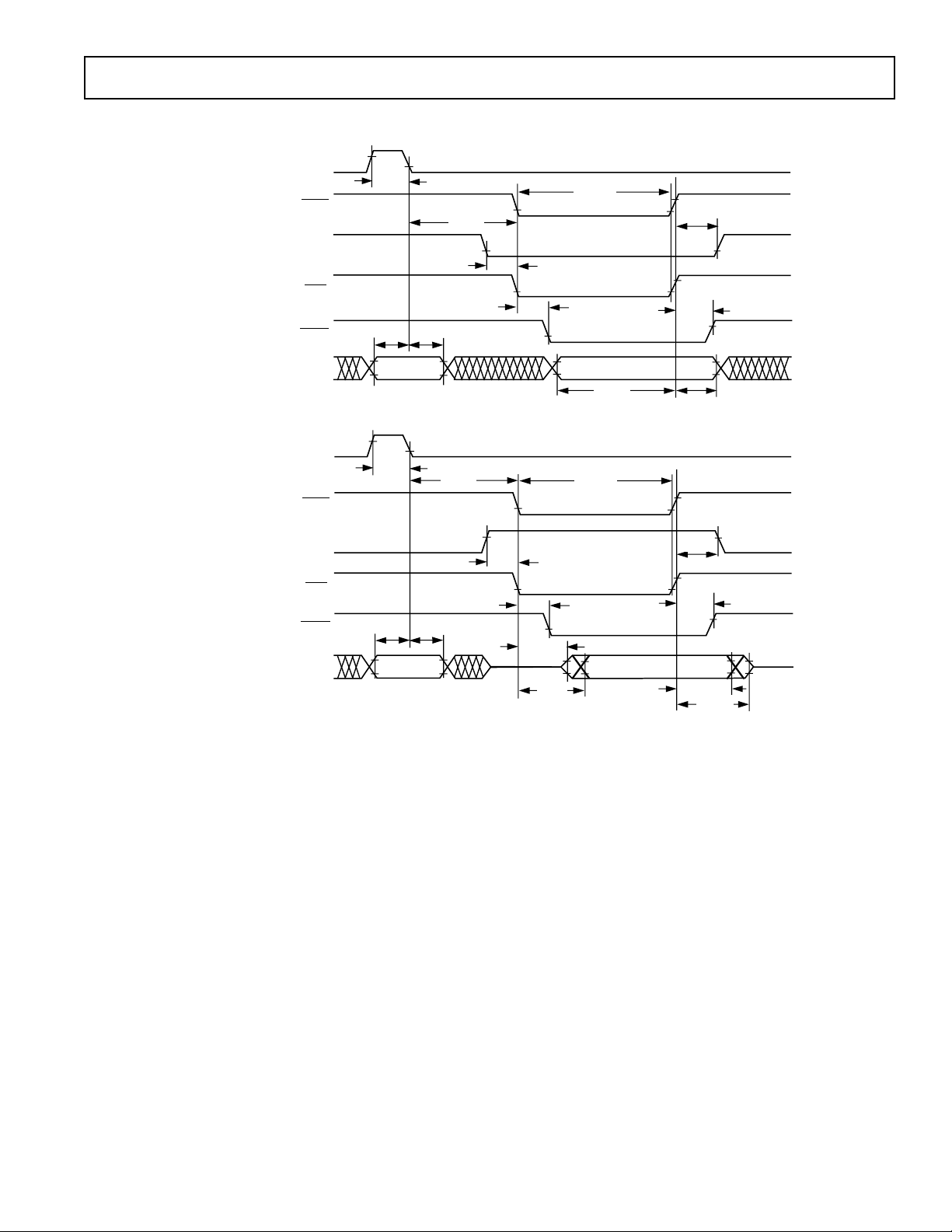
Host Write Cycle
ALE
HSEL
HRW
HDS
HACK
t
t
HALP
HASU
ADSP-21xx
t
HRWP
t
t
HALS
t
HSU
t
HSHK
t
HAH
HH
t
HKH
Host Read Cycle
HD15–0
ALE
HSEL
HRW
HDS
HACK
HD15–0
ADDRESS
t
HALP
t
HASU
ADDRESS
t
HAH
t
HALS
t
HDSU
t
HRWP
t
HSU
t
HSHK
t
HDE
t
HDD
Figure 38. Host Interface Port (HMD1 = 1, HMD0 = 1)
DATA
DATA
t
HWDH
t
t
HKH
t
HH
HRDH
t
HRDD
REV. B
–43–

ADSP-21xx
TIMING PARAMETERS (ADSP-2103/2162/2164)
GENERAL NOTES
Use the exact timing information given. Do not attempt to
derive parameters from the addition or subtraction of others.
While addition or subtraction would yield meaningful results for
an individual device, the values given in this data sheet reflect
statistical variations and worst cases. Consequently, you cannot
meaningfully add parameters to derive longer times.
TIMING NOTES
Timing requirements apply to signals that are controlled by
circuitry external to the processor, such as the data input for a
read operation. Timing requirements guarantee that the
processor operates correctly with other devices.
MEMORY REQUIREMENTS
The table below shows common memory device specifications
and the corresponding ADSP-21xx timing parameters, for your
convenience.
Switching characteristics specify how the processor changes its
signals. You have no control over this timing—circuitry external
to the processor must be designed for compatibility with these
signal characteristics. Switching characteristics tell you what the
processor will do in a given circumstance. You can also use
switching characteristics to ensure that any timing requirement
of a device connected to the processor (such as memory) is
satisfied.
ADSP-21xx
Memory Specification Timing Parameter Timing Parameter Definition
Address Setup to Write Start t
Address Setup to Write End t
Address Hold Time t
Data Setup Time t
Data Hold Time t
OE to Data Valid t
Address Access Time t
ASW
AW
WRA
DW
DH
RDD
AA
A0–A13, DMS, PMS Setup before WR Low
A0–A13, DMS, PMS Setup before WR Deasserted
A0–A13, DMS, PMS Hold after WR Deasserted
Data Setup before WR High
Data Hold after WR High
RD Low to Data Valid
A0–A13, DMS, PMS, BMS to Data Valid
–44–
REV. B

ADSP-21xx
TIMING PARAMETERS (ADSP-2103/2162/2164)
CLOCK SIGNALS & RESET
Frequency
10.24 MHz Dependency
Parameter Min Max Min Max Unit
Timing Requirement:
t
CK
t
CKL
t
CKH
t
RSP
Switching Characteristic:
t
CPL
t
CPH
t
CKOH
NOTES
1
Applies after powerup sequence is complete. Internal phase lock loop requires no more than 2000 CLKIN cycles assuming stable CLKIN (not including crystal
oscillator startup time).
CLKIN Period 97.6 150 ns
CLKIN Width Low 20 ns
CLKIN Width High 20 ns
RESET Width Low 488 5t
CK
1
ns
CLKOUT Width Low 38.8 0.5tCK – 10 ns
CLKOUT Width High 38.8 0.5tCK – 10 ns
CLKIN High to CLKOUT High 0 20 ns
t
CK
t
CKH
CLKIN
CLKOUT
t
CKL
t
CKOH
t
CPH
t
CPL
Figure 39. Clock Signals
REV. B
–45–

ADSP-21xx
TIMING PARAMETERS (ADSP-2103/2162/2164)
INTERRUPTS & FLAGS
Frequency
10.24 MHz Dependency
Parameter Min Max Min Max Unit
Timing Requirement:
t
t
IFS
IFH
IRQx1 or FI Setup before CLKOUT Low
IRQx1 or FI Hold after CLKOUT High
2, 3
2, 3
44.4 0.25tCK + 20 ns
24.4 0.25t
CK
ns
Switching Characteristic:
t
FOH
t
FOD
NOTES
1
IRQx=IRQ0, IRQ1, and IRQ2.
2
If IRQx and FI inputs meet t
following cycle. (Refer to the “Interrupt Controller” section in Chapter 3, Program Control, of the ADSP-2100 Family User’s Manual for further information on
interrupt servicing.)
3
Edge-sensitive interrupts require pulse widths greater than 10 ns. Level-sensitive interrupts must be held low until serviced.
FO Hold after CLKOUT High 0 ns
FO Delay from CLKOUT High 15 ns
and t
IFS
setup/hold requirements, they will be recognized during the current clock cycle; otherwise they will be recognized during the
IFH
CLKOUT
FLAG
OUTPUT(S)
IRQx
FI
t
FOH
t
FOD
t
IFH
t
IFS
Figure 40. Interrupts & Flags
–46–
REV. B
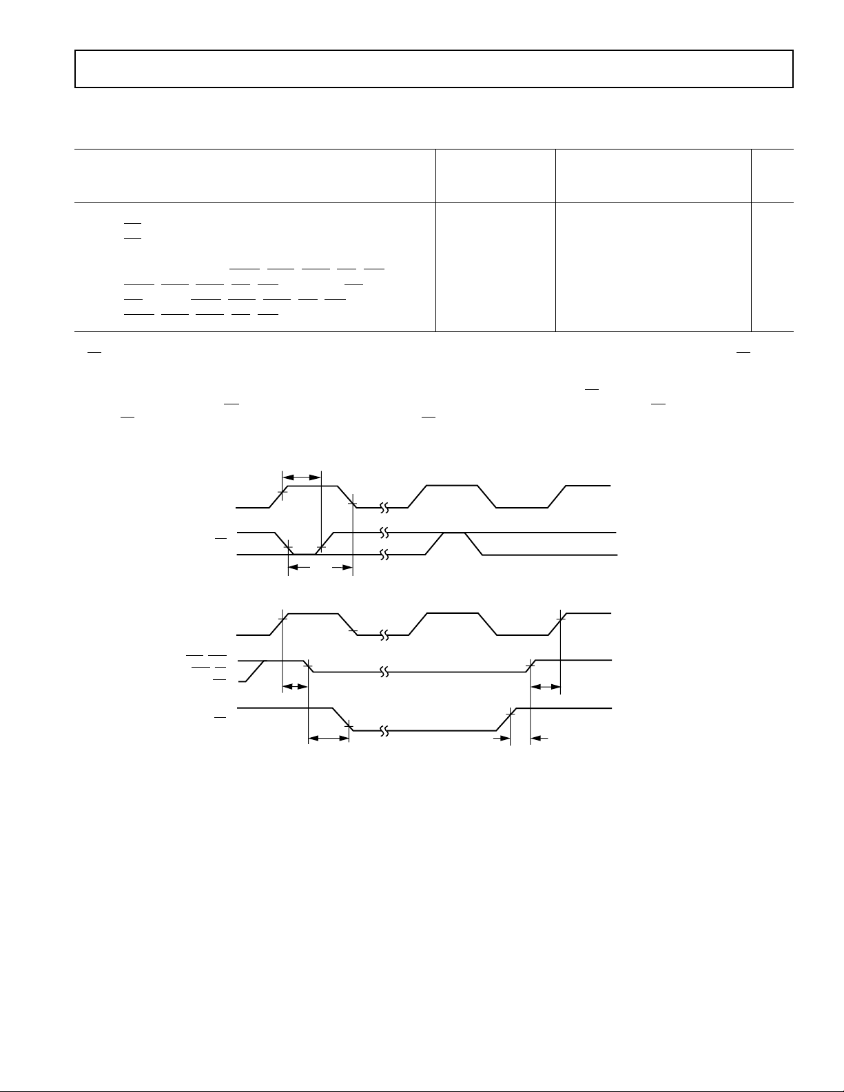
ADSP-21xx
TIMING PARAMETERS (ADSP-2103/2162/2164)
BUS REQUEST/GRANT
Frequency
10.24 MHz Dependency
Parameter Min Max Min Max Unit
Timing Requirement:
t
BH
t
BS
BR Hold after CLKOUT High
BR Setup before CLKOUT Low
1
1
29.4 0.25tCK + 5 ns
44.4 0.25tCK + 20 ns
Switching Characteristic:
t
SD
t
SDB
t
SE
t
SEC
NOTES
1
If BR meets the tBS and tBH setup/hold requirements, it will be recognized in the current processor cycle; otherwise it is recognized in the following cycle. BR
requires a pulse width greater than 10 ns.
Section 10.2.4, “Bus Request/Grant,” of the ADSP-2100 Family User’s Manual (1st Edition, ©1993) states that “When BR is recognized, the processor
responds immediately by asserting BG during the same cycle.” This is incorrect for the current versions of all ADSP-21xx processors: BG is asserted in the
cycle after BR is recognized. No external synchronization circuit is needed when BR is generated as an asynchronous signal.
CLKOUT High to DMS, PMS, BMS, RD, WR Disable 44.4 0.25tCK + 20 ns
DMS, PMS, BMS, RD, WR Disable to BG Low 0 ns
BG High to DMS, PMS, BMS, RD, WR Enable 0 ns
DMS, PMS, BMS, RD, WR Enable to CLKOUT High 14.4 0.25tCK – 10 ns
t
BH
CLKOUT
BR
t
BS
CLKOUT
PMS, DMS
BMS, RD
WR
BG
t
SD
t
SDB
t
SEC
t
SE
Figure 41. Bus Request/Grant
REV. B
–47–

ADSP-21xx
TIMING PARAMETERS (ADSP-2103/2162/2164)
MEMORY READ
Frequency
10.24 MHz Dependency
Parameter Min Max Min Max Unit
Timing Requirement:
t
RDD
t
AA
t
RDH
Switching Characteristic:
t
RP
t
CRD
t
ASR
t
RDA
t
RWR
w = wait states × t
RD Low to Data Valid 33.8 0.5tCK – 15 + w ns
A0–A13, PMS, DMS, BMS to Data Valid 49.2 0.75tCK – 24 + w ns
Data Hold from RD High 0 ns
RD Pulse Width 43.8 0.5tCK – 5 + w ns
CLKOUT High to RD Low 19.4 34.4 0.25tCK – 5 0.25tCK + 10 ns
A0–A13, PMS, DMS, BMS Setup before RD Low 12.4 0.25tCK – 12 ns
A0–A13, PMS, DMS, BMS Hold after RD Deasserted 14.4 0.25tCK – 10 ns
RD High to RD or WR Low 38.8 0.5tCK – 10 ns
CK.
CLKOUT
A0 – A13
DMS, PMS
BMS
RD
WR
t
RDA
t
RDD
t
RP
t
RWR
t
RDH
t
ASR
t
CRD
D
t
AA
Figure 42. Memory Read
–48–
REV. B

ADSP-21xx
TIMING PARAMETERS (ADSP-2103/2162/2164)
MEMORY WRITE
Frequency
10.24 MHz Dependency
Parameter Min Max Min Max Unit
Switching Characteristic:
t
DW
t
DH
t
WP
t
WDE
t
ASW
t
DDR
t
CWR
t
AW
t
WRA
t
WWR
w = wait states × t
Data Setup before WR High 38.8 0.5t
Data Hold after WR High 14.4 0.25t
– 10 + w ns
CK
– 10 ns
CK
WR Pulse Width 43.8 0.5tCK – 5 + w ns
WR Low to Data Enabled 0
A0–A13, DMS, PMS Setup before WR Low 12.4 0.25t
– 12 ns
CK
Data Disable before WR or RD Low 14.4 0.25tCK – 10 ns
CLKOUT High to WR Low 19.4 34.4 0.25t
A0–A13, DMS, PMS, Setup before WR Deasserted 58.2 0.75t
A0–A13, DMS, PMS Hold After WR Deasserted 14.4 0.25t
– 5 0.25tCK + 10 ns
CK
– 15 + w ns
CK
– 10 ns
CK
WR High to RD or WR Low 38.8 0.5tCK – 10 ns
CK.
CLKOUT
A0 – A13
DMS, PMS
WR
RD
t
WRA
t
WDE
t
WP
t
AW
t
DW
t
WWR
t
DH
t
DDR
t
ASW
t
CWR
D
Figure 43. Memory Write
REV. B
–49–

ADSP-21xx
TIMING PARAMETERS (ADSP-2103/2162/2164)
SERIAL PORTS
Frequency
10.24 MHz Dependency
Parameter Min Max Min Max Unit
Timing Requirement:
t
SCK
t
SCS
t
SCH
t
SCP
Switching Characteristic:
t
CC
t
SCDE
t
SCDV
t
RH
t
RD
t
SCDH
t
TDE
t
TDV
t
SCDD
t
RDV
SCLK Period 97.6 t
CK
ns
DR/TFS/RFS Setup before SCLK Low 8 ns
DR/TFS/RFS Hold after SCLK Low 10 ns
SCLK
CLKOUT High to SCLK
Width 28 ns
in
out
24.4 39.4 0.25t
CK
0.25t
+ 15 ns
CK
SCLK High to DT Enable 0 ns
SCLK High to DT Valid 28 ns
TFS/RFS
TFS/RFS
Hold after SCLK High 0 ns
out
Delay from SCLK High 28 ns
out
DT Hold after SCLK High 0 ns
TFS (alt) to DT Enable 0 ns
TFS (alt) to DT Valid 18 ns
SCLK High to DT Disable 30 ns
RFS (Multichannel, Frame Delay Zero) 20 ns
to DT Valid
CLKOUT
SCLK
DR
RFS
TFS
RFS
OUT
TFS
OUT
DT
TFS
( ALTERNATE
FRAME MODE )
( MULTICHANNEL MODE,
FRAME DELAY 0 {MFD = 0} )
RFS
t
CC
IN
IN
t
t
SCDE
t
RD
t
RH
SCDV
t
TDE
t
TDV
t
CC
t
SCDD
t
t
t
SCS
SCH
t
SCDH
t
RDV
SCP
t
SCK
t
SCP
Figure 44. Serial Ports
–50–
REV. B

PIN CONFIGURATIONS
68-Pin PGA
ADSP-21xx
L K J H G F E D C B A
BR
1
A5
2
GND
3
A8
4
A10
5
A12
6
PMS
7
BMS
8
XTAL
9
CLK
10
OUT
11
L K J H G F E D C B A
V
A6
A7
A9
A11
A13
DMS
BG
CLK
RD
WR
A3
DD
IRQ2
A0
A2
A4
PGA PACKAGE
ADSP-2101
TOP VIEW
(PINS DOWN)
IN
TFS0
DT0
GND
RFS0
SCLK0
DR0
IRQ1
(TFS1)
FO
(DT1)
RESET
A1
V
DD
MMAP
FI
(DR1)
IRQ0
(RFS1)
D22
D23
V
DD
SCLK1
D20
D21
INDEX
(NC)
D1
D0
GND
D19
D17
D15
D13
GND
D10
D8
D6
D4
D2
D18
D16
D14
D12
D11
LKJHGFEDCBA
1
2
3
4
5
6
7
D9
8
D7
9
D5
10
D3
11
1
GND
2
3
4
5
6
7
8
9
10
11
D18
D16
D14
D12
D11
D19
D17
D15
D13
GND
D10
D9
D8
D7
D6
D5
D4
D3
D2
D20
D21
INDEX
(NC)
D1
D0
D22
D23
PGA PACKAGE
V
DD
SCLK1
BR
V
DD
IRQ2
MMAP
ADSP-2101
BOTTOM VIEW
(PINS UP)
IRQ1
FI
(TFS1)
(DR1)
IRQ0
FO
(RFS1)
(DT1)
RESET
A0
SCLK0
DR0
A1
A2
GND
RFS0
A3
A4
TFS0
DT0
NC = NO CONNECT
V
A6
A7
A9
A11
A13
DMS
BG
CLK
RD
WR
DD
IN
A5
GND
A8
A10
A12
PMS
BMS
XTAL
CLK
OUT
LKJHGFEDCBA
1
2
3
4
5
6
7
8
9
10
11
PGA Pin
Number Name
K11
WR
K10 RD
J11 DT0
J10 TFS0
H11 RFS0
H10 GND
G11 DR0
G10 SCLK0
F11 FO (DT1)
F10
E11
IRQ1 (TFS1)
IRQ0 (RFS1)
E10 FI (DR1)
D11 SCLK1
D10 V
DD
C11 D0
C10 D1
B11 D2
PGA Pin
Number Name
A10 D3
B10 D4
A9 D5
B9 D6
A8 D7
B8 D8
A7 D9
B7 D10
A6 D11
B6 GND
A5 D12
B5 D13
A4 D14
B4 D15
A3 D16
B3 D17
A2 D18
PGA Pin
Number Name
B1 GND
B2 D19
C1 D20
C2 D21
D1 D22
D2 D23
E1 V
DD
E2 MMAP
F1
BR
F2 IRQ2
G1
RESET
G2 A0
H1 A1
H2 A2
J1 A3
J2 A4
K1 V
DD
PGA Pin
Number Name
L2 A5
K2 A6
L3 GND
K3 A7
L4 A8
K4 A9
L5 A10
K5 A11
L6 A12
K6 A13
L7
K7
PMS
DMS
L8 BMS
K8
BG
L9 XTAL
K9 CLKIN
L10 CLKOUT
C3 Index (NC)
REV. B
–51–

ADSP-21xx
D18
9
D17
8
PIN CONFIGURATIONS
68-Lead PLCC
D16
D15
D14
D13
D12
GND
D11
7
6
5
4
3
2
1
D10D9D8D7D6D5D4
68676665646362
D3
61
GND
D19
D20
D21
D22
D23
V
MMAP
BR
IRQ2
RESET
V
10
11
12
13
14
15
16
DD
17
18
19
20
A0
21
A1
22
A2
23
A3
24
A4
25
26
DD
272829
A5
A6
GND
PLCC PACKAGE
ADSP-2161/62/63/64
3031323334
A7A8A9
PIN 1
IDENTIFIER
ADSP-2101
ADSP-2103
ADSP-2105
ADSP-2115
TOP VIEW
(PINS DOWN)
3536373839
A10
A11
A12
A13
PMS
DMS
BMS
404142
BG
XTAL
CLKIN
43
CLKOUT
60
D2
59
D1
58
D0
57
V
DD
56
SCLK1
55
(DR1)
FI
54
IRQ0
(RFS1)
53
IRQ1
(TFS1)
52
FO
(DT1)
51
SCLK0
50
DR0
(NC on ADSP-2105)
49
GND
48
47
46
45
44
(NC on ADSP-2105)
RFS0
TFS0
(NC on ADSP-2105)
DT0
(NC on ADSP-2105)
RD
WR
NC = NO CONNECT
(NC on ADSP-2105)
PLCC Pin
Number Name
1 D11
2 GND
3 D12
4 D13
5 D14
6 D15
7 D16
8 D17
9 D18
10 GND
11 D19
12 D20
13 D21
14 D22
15 D23
16 V
DD
17 MMAP
PLCC Pin
Number Name
18
19
BR
IRQ2
20 RESET
21 A0
22 A1
23 A2
24 A3
25 A4
26 V
DD
27 A5
28 A6
29 GND
30 A7
31 A8
32 A9
33 A10
34 A11
PLCC Pin
Number Name
35 A12
36 A13
37
PMS
38 DMS
39
BMS
40 BG
41 XTAL
42 CLKIN
43 CLKOUT
44
45
WR
RD
46 DT0 (NC on ADSP-2105)
47 TFS0 (NC on ADSP-2105)
48 RFS0 (NC on ADSP-2105)
49 GND
50 DR0 (NC on ADSP-2105)
51 SCLK0 (NC on ADSP-2105)
–52–
PLCC Pin
Number Name
52 FO (DT1)
53
54
IRQ1 (TFS1)
IRQ0 (RFS1)
55 FI (DR1)
56 SCLK1
57 V
DD
58 D0
59 D1
60 D2
61 D3
62 D4
63 D5
64 D6
65 D7
66 D8
67 D9
68 D10
REV. B

DDVDD
V
PIN CONFIGURATIONS
80-Lead PQFP
80-Lead TQFP
A4A3A2A1A0
RESET
IRQ2BRMMAP
VDDVDDD23
D22
D21
D20
D19
GND
ADSP-21xx
GND
GND
GND
A10
A11
A12
A13
PMS
DMS
BMS
BG
XTAL
CLKIN
NC
NC
NC
80797877767574737271706968676665646362
A5
A6
A7
A8
A9
80797877767574737271706968676665646362
1
2
3
4
5
6
7
8
9
10
11
12
13
14
15
16
17
18
19
20
21222324252627282930313233343536373839
RD
WR
DT0
CLKOUT
PQFP PACKAGE
ADSP-2101
ADSP-2103
ADSP-2115
ADSP-2161/62/63/64
TOP VIEW
(PINS DOWN)
DR0
GND
RFS0
GND
SCLK0
TFS0
(DT1)
FO
(TFS1)
(RFS1)
IRQ1
IRQ0
(DR1)
F1
SCLK1
DD
V
D0D1D2
61
61
60
59
58
57
56
55
54
53
52
51
50
49
48
47
46
45
44
43
42
41
40
D3
NC = NO CONNECT
D18
D17
D16
D15
D14
D13
D12
GND
GND
D11
D10
D9
D8
D7
D6
D5
D4
NC
NC
NC
PQFP/
TQFP Pin
Number Name
1A5
2A6
3 GND
4 GND
5A7
6A8
7A9
8 A10
9 A11
10 A12
11 A13
12
PMS
13 DMS
14
BMS
15 BG
16 XTAL
17 CLKIN
18 NC
19 NC
20 NC
REV. B
PQFP/
TQFP Pin
Number Name
21 CLKOUT
22
WR
23 RD
24 DT0
25 TFS0
26 RFS0
27 GND
28 GND
29 DR0
30 SCLK0
31 FO (DT1)
32
IRQ1 (TFS1)
33 IRQ0 (RFS1)
34 FI (DR1)
35 SCLK1
36 V
DD
37 D0
38 D1
39 D2
40 D3
–53–
PQFP/
TQFP Pin
Number Name
41 NC
42 NC
43 NC
44 D4
45 D5
46 D6
47 D7
48 D8
49 D9
50 D10
51 D11
52 GND
53 GND
54 D12
55 D13
56 D14
57 D15
58 D16
59 D17
60 D18
PQFP/
TQFP Pin
Number Name
61 GND
62 GND
63 D19
64 D20
65 D21
66 D22
67 D23
68 V
69 V
DD
DD
70 MMAP
71 BR
72
IRQ2
73 RESET
74 A0
75 A1
76 A2
77 A3
78 A4
79 V
80 V
DD
DD

ADSP-21xx
PIN CONFIGURATIONS
100-Pin PGA
13 12 11 10 9 8 7 5 46321
N
M
RESETBR
L
PMS
V
K
J
H
G
F
E
D
C
B
A
DD
BMSBGDMS
WR RD
A5A4A3 DT0
A6GND BMODE
A8A7 HMD1 HMD0
DD
13 12 11 10 9 8 7 5 46321
D15 GND D8 FL2 FL0
PGA PACKAGE
ADSP-2111
TOP VIEW
(PINS DOWN)
HD9 HD7 XTALA11A9 HSIZE
HD4HD15A12A10
DD
D5D7 D3D18 D16 D13 D12 D10D20D21D23 D1 V
D4D6 D2D19 D17 D14 D11 D9D22GNDMMAP D0 FL1
INDEX
HD1HD3 HA1HD13 HD11 HD8 V
CLK
HD2
IN
SCLK1
(DR1)
IRQ0
(TFS1)
(RFS1)
FO
GND SCLK0
(DT1)
RFSOA1A0A2 TFS0 DR0
CLK
HACK
OUT
HRD/
PIN
HRW
(NC)
HWR/
HSEL
HA2/
HD0HD12 HD10 GND HD6 HD5HD14A13V
ALE
DD
F1
IRQ1
IRQ2
HDS
HA0
N
M
L
K
J
H
G
F
E
D
C
B
A
V
DD
N
M
FL0
L
F1
SCLK1
K
(DR1)
IRQ1
J
(RFS1)
(TFS1)
SCLK0
H
G
DT0
F
IRQ2
BMODE
E
HMD0
D
HSIZE
C
HWR/
B
HDS
A
D1
FL2
IRQ0
GND
CLK
OUT
HMD1
HRD/
HRW
HSEL
HA2/
ALE
FO
(DT1)
RFSODR0 TFS0
HACK
INDEX
PIN
(NC)
HA1
HD0
D4 D6D2 D19D17D11 D22D14D9
PGA PACKAGE
ADSP-2111
BOTTOM VIEW
(PINS UP)
HD1 HD3
CLK
HD2
IN
D12D5 D7D3 D18D16 D20D13D10 D23D21
GNDFL1 D0
D15GNDD8
HD9HD7XTAL
V
DD
HD11 HD13 HD15HD8HD4 A10A12
HD10HD6 HD12 HD14GNDHD5
RESET
DMS
RD
A1
A5
NC = NO CONNECT
13121110987546321
13121110987546321
N
MMAP
M
BR
L
V
PMS
DD
WR
A0
A4
A6
A8
A11
A13HA0
BMS
GND
K
J
BG
H
A2
G
A3
F
E
A7
D
A9
C
B
V
DD
A
13121110987546321
PGA Pin
Number Name
N13 D23
N12 D21
M13 MMAP
M12 GND
L13
BR
L12 RESET
K13
K12 V
PMS
DD
J13 BMS
J12 DMS
H13
BG
H12 WR
H11
RD
G13 A2
G12 A0
G11 A1
F13 A3
F12 A4
F11 A5
E13 GND
E12 A6
D13 A7
D12 A8
C13 A9
C12 A11
PGA Pin
Number Name
B13 A10
A13 V
DD
A12 A13
B12 A12
A11 HD14
B11 HD15
A10 HD12
B10 HD13
A9 HD10
B9 HD11
A8 GND
B8 HD8
C8 HD9
A7 HD6
B7 V
DD
C7 HD7
A6 HD5
B6 HD4
C6 XTAL
A5 CLKIN
B5 HD3
A4 HD2
B4 HD1
A3 HD0
B3 HA1
PGA Pin
Number Name
C3 Index (NC)
A2 HA2/ALE
A1 HA0
B1 HWR/HDS
B2
HSEL
C1 HSIZE
C2
HRD/HRW
D1 HMD0
D2 HMD1
E1
IRQ2
E2 BMODE
F1 DT0
F2 CLKOUT
F3
HACK
G1 DR0
G2 TFS0
G3 RFS0
H1 SCLK0
H2 GND
H3 FO (DT1)
J1
IRQ1 (TFS1)
J2 IRQ0 (RFS1)
K1 FI (DR1)
K2 SCLK1
L1 FL0
PGA Pin
Number Name
L2 FL2
M1 FL1
N1 V
DD
N2 D1
M2 D0
N3 D3
M3 D2
N4 D5
M4 D4
N5 D7
M5 D6
N6 D10
M6 D9
L6 D8
N7 D12
M7 D11
L7 GND
N8 D13
M8 D14
L8 D15
N9 D16
M9 D17
N10 D18
M10 D19
N11 D20
M11 D22
–54–
REV. B

GND
MMAP
RESET
BR
V
PMS
DMS
BMS
RD
WR
BG
GND
A10
A11
VDD
ADSP-21xx
PIN CONFIGURATIONS
100-Lead Bumpered PQFP
D23
D22
D21
D20
D19
D18
D17
D16
D15
D14
D13
D12
GND
D11
D10D9D8D7D6D5D4D3D2D1D0
987654321
131211
14
15
16
17
DD
A0
A1
A2
A3
A4
A5
A6
A7
A8
A9
18
19
20
21
22
23
24
25
26
27
28
29
30
31
32
33
34
35
36
37
38
10
BEVELED EDGE
PQFP PACKAGE
ADSP-2111
(PINS DOWN)
39404142434445464748495051525354555657585960616263
9998979695949392919089
100
TOP VIEW
88
87
86
85
84
83
82
81
80
79
78
77
76
75
74
73
72
71
70
69
68
67
66
65
64
VDD
FL2
FL1
FL0
SCLK1
FI
(DR1)
IRQ0
(RFS1)
IRQ1
(TFS1)
FO
(DT1)
GND
SCLK0
DR0
RFS0
TFS0
DT0
CLKOUT
HACK
IRQ2
BMODE
HMD0
HMD1
HSIZE
HRD/HRW
HWR/HDS
HSEL
PQFP Pin
Number Name
1 GND
2 D12
3 D13
4 D14
5 D15
6 D16
7 D17
8 D18
9 D19
10 D20
11 D21
12 D22
13 D23
14 GND
15 MMAP
16
17
18 V
RESET
BR
DD
19 PMS
20 DMS
21
BMS
22 RD
23
WR
24 BG
25 A0
A12
A13
HD15
HD14
NOTE: PIN 1 IS LOCATED AT THE CENTER OF THE BEVELED-EDGE SIDE OF THE PACKAGE.
PQFP Pin
Number Name
26 A1
27 A2
28 A3
29 A4
30 A5
31 GND
32 A6
33 A7
34 A8
35 A9
36 A10
37 A11
38 V
DD
39 A12
40 A13
41 HD15
42 HD14
43 HD13
44 HD12
45 HD11
46 HD10
47 HD9
48 HD8
49 GND
50 V
DD
HD13
HD12
HD11
HD10
HD9
HD8
HD7
HD6
HD5
HD4
VDD
GND
XTAL
PQFP Pin
Number Name
51 HD7
52 HD6
53 HD5
54 HD4
55 XTAL
56 CLKIN
57 HD3
58 HD2
59 HD1
60 HD0
61 HA2/ALE
62 HA1
63 HA0
64
65
66 HRD/HRW
67 HSIZE
68 HMD1
69 HMD0
70 BMODE
71
72 HACK
73 CLKOUT
74 DT0
75 TFS0
HD3
HD2
HD1
CLKIN
HSEL
HWR/HDS
IRQ2
HD0
HA2/ALE
HA1
HA0
PQFP Pin
Number Name
76 RFS0
77 DR0
78 SCLK0
79 GND
80 FO (DT1)
81
82
IRQ1 (TFS1)
IRQ0 (RFS1)
83 FI (DR1)
84 SCLK1
85 FL0
86 FL1
87 FL2
88 V
DD
89 D0
90 D1
91 D2
92 D3
93 D4
94 D5
95 D6
96 D7
97 D8
98 D9
99 D10
100 D11
REV. B
–55–

ADSP-21xx
OUTLINE DIMENSIONS
ADSP-2101
68-Pin Grid Array (PGA)
PGA LOCATION A1 QUADRANT MARKING
D
D
PLANE
A
φ
b
e
SEATING
INCHES MILLIMETERS
SYMBOL MIN TYP MAX MIN TYP MAX
e
1
e
2
1
2
GUIDE
PIN ONLY
e
1
e
2
A
1
L
3
φ
b
1
TOP VIEW
3
4
5
6
7
8
9
10
11
ABCDEFGHJKL
A 0.123 0.164 3.12 4.17
A
1
0.50 1.27
φb 0.016 0.018 0.020 0.46
φb
1
0.050 1.27
D 1.086 1.110 27.58 28.19
e
1
e
2
0.988 1.012 25.10 25.70
0.788 0.812 20.02 20.62
e 0.100 2.54
L
3
0.180 4.57
–56–
REV. B

OUTLINE DIMENSIONS
ADSP-21xx
68-Lead Plastic Leaded Chip Carrier (PLCC)
ADSP-21xx
9
PIN 1 IDENTIFIER
TOP VIEW
(PINS DOWN)
D
1
D
61
e
D
2
b
BOTTOM VIEW
(PINS UP)
b
1
D
A
1
A
INCHES MILLIMETERS
SYMBOL MIN TYP MAX MIN TYP MAX
A 0.169 0.172 0.175 4.29 14.37 4.45
A
1
0.104 12.64
b 0.017 0.018 0.019 0.43 10.46 0.48
b
1
0.027 0.028 0.029 0.69 10.71 0.74
D 0.985 0.990 0.995 25.02 25.15 25.27
D
1
D
2
0.950 0.952 0.954 24.13 24.18 24.23
0.895 0.910 0.925 22.73 23.11 23.50
e 0.050 11.27
D
0.004 10.10
REV. B
–57–

ADSP-21xx
OUTLINE DIMENSIONS
ADSP-21xx
80-Lead Metric Plastic Quad Flatpack (PQFP)
80-Lead Metric Thin Quad Flatpack (TQFP)
SEATING
PLANE
D
D
A
L
80 61
1
D
A
2
A
1
20
1
D
3
TOP VIEW
(PINS DOWN)
e
60
E
E
41
4021
B
E
1
3
PQFP TQFP
MILLIMETERS INCHES
SYMBOL MIN TYP MAX MIN TYP MAX
A 2.45 0.096
A
1
A
2
0.25 0.010
1.90 2.00 2.10 0.075 0.079 0.083
D, E 16.95 17.20 17.45 0.667 0.678 0.690
D1, E
D3, E
1
3
13.90 14.00 14.10 0.547 0.551 0.555
12.35 12.43 0.486 0.490
L 0.65 0.80 0.95 0.026 0.031 0.037
e 0.57 0.65 0.73 0.023 0.026 0.029
B 0.22 0.30 0.38 0.009 0.012 0.015
D
0.10 0.004
–58–
MILLIMETERS INCHES
MIN TYP MAX MIN TYP MAX
1.60 0.063
0.05 0.15 0.002 0.006
1.35 1.40 1.45 0.053 0.055 0.057
15.75 16.00 16.25 0.620 0.630 0.640
13.95 14.00 14.05 0.549 0.551 0.553
12.35 12.43 0.486 0.490
0.50 0.60 0.75 0.020 0.024 0.030
0.57 0.65 0.73 0.022 0.026 0.029
0.25 0.30 0.35 0.010 0.012 0.014
0.10 0.004
REV. B

PGA LOCATION A1 QUADRANT MARKING
D
A
SEATING
PLANE
φ b
ADSP-21xx
OUTLINE DIMENSIONS
ADSP-2111
100-Pin Grid Array (PGA)
e
1
e
2
1
2
3
INDEX
PIN
ONLY
e
e
2
1
D
e
φ b
A
1
L
3
1
TOP VIEW
4
5
6
7
8
9
10
11
12
13
ABCDEFGHJKLNM
REV. B
INCHES MILLIMETERS
SYMBOL MIN TYP MAX MIN TYP MAX
A 0.123 0.169 3.12 4.29
A
1
0.050 1.27
φb 0.016 0.018 0.020 0.41 0.46 0.51
φb
1
0.050 1.27
D 1.308 1.32 1.342 33.22 33.53 34.09
e
1
e
2
1.188 1.20 1.212 30.18 30.48 30.78
0.988 1.00 1.012 25.10 25.4 25.70
e 0.100 2.54
L
3
0.180 4.57
–59–

ADSP-21xx
SEATING
PLANE
D3, E
OUTLINE DIMENSIONS
ADSP-2111
100-Lead Bumpered Plastic Quad Flatpack (PQFP)
D
2
D
D
A
L
14
3
13
Beveled
Edge
1
1
TOP VIEW
(PINS DOWN)
89
88
E2E
E
1
38
D
A
2
A
1
NOTE: PIN 1 IS THE CENTER PIN ON THE BEVELED-EDGE SIDE OF THE PACKAGE.
39 63
e
B
64
INCHES MILLIMETERS
SYMBOL MIN TYP MAX MIN TYP MAX
A 0.180 4.572
A
1
A
2
0.020 0.030 0.040 0.508 0.762 1.016
0.130 0.140 0.150 3.302 3.556 3.810
D, E 0.875 0.880 0.885 22.225 22.352 22.479
D1, E
D2, E
D3, E
1
2
3
0.747 0.750 0.753 18.974 19.050 19.126
0.897 0.900 0.903 22.784 22.860 22.936
0.600 0.603 15.240 15.316
L 0.036 0.046 0.914 1.168
e 0.022 0.025 0.028 0.559 0.635 0.711
B 0.008 0.012 0.203 0.305
D
0.004 0.102
–60–
REV. B

ADSP-21xx
ORDERING GUIDE
Ambient
Part Number
1
ADSP-2101KG-66 0°C to +70°C 16.67 MHz 68-Pin PGA G-68A
ADSP-2101BG-66 –40°C to +85°C 16.67 MHz 68-Pin PGA G-68A
ADSP-2101KP-66 0°C to +70°C 16.67 MHz 68-Lead PLCC P-68A
ADSP-2101BP-66 –40°C to +85°C 16.67 MHz 68-Lead PLCC P-68A
ADSP-2101KS-66 0°C to +70°C 16.67 MHz 80-Lead PQFP S-80
ADSP-2101BS-66 –40°C to +85°C 16.67 MHz 80-Lead PQFP S-80
ADSP-2101KG-80 0°C to +70°C 20.0 MHz 68-Pin PGA G-68A
ADSP-2101BG-80 –40°C to +85°C 20.0 MHz 68-Pin PGA G-68A
ADSP-2101KP-80 0°C to +70°C 20.0 MHz 68-Lead PLCC P-68A
ADSP-2101BP-80 –40°C to +85°C 20.0 MHz 68-Lead PLCC P-68A
ADSP-2101KS-80 0°C to +70°C 20.0 MHz 80-Lead PQFP S-80
ADSP-2101BS-80 –40°C to +85°C 20.0 MHz 80-Lead PQFP S-80
ADSP-2101KP-100 0°C to +70°C 25.0 MHz 68-Pin PLCC P-68A
ADSP-2101BP-100 –40°C to +85°C 25.0 MHz 68-Pin PLCC P-68A
ADSP-2101KS-100 0°C to +70°C 25.0 MHz 80-Lead PQFP S-80
ADSP-2101BS-100 –40°C to +85°C 25.0 MHz 80-Lead PQFP S-80
ADSP-2101KG-100 0°C to +70°C 25.0 MHz 68-Lead PGA G-68A
ADSP-2101BG-100 –40°C to +85°C 25.0 MHz 68-Lead PGA G-68A
ADSP-2101TG-50 –55°C to +125°C 12.5 MHz 68-Pin PGA G-68A
ADSP-2103KP-40 (3.3 V) 0°C to +70°C 10.24 MHz 68-Lead PLCC P-68A
ADSP-2103BP-40 (3.3 V) –40°C to +85°C 10.24 MHz 68-Lead PLCC P-68A
ADSP-2103KS-40 (3.3 V) 0°C to +70°C 10.24 MHz 80-Lead PQFP S-80
ADSP-2103BS-40 (3.3 V) –40°C to +85°C 10.24 MHz 80-Lead PQFP S-80
ADSP-2105KP-55 0°C to +70°C 13.824 MHz 68-Lead PLCC P-68A
ADSP-2105BP-55 –40°C to +85°C 13.824 MHz 68-Lead PLCC P-68A
ADSP-2105KP-80 0°C to +70°C 20.0 MHz 68-Lead PLCC P-68A
ADSP-2105BP-80 –40°C to +85°C 20.0 MHz 68-Lead PLCC P-68A
ADSP-2115KP-66 0°C to +70°C 16.67 MHz 68-Lead PLCC P-68A
ADSP-2115BP-66 –40°C to +85°C 16.67 MHz 68-Lead PLCC P-68A
ADSP-2115KS-66 0°C to +70°C 16.67 MHz 80-Lead PQFP S-80
ADSP-2115BS-66 –40°C to +85°C 16.67 MHz 80-Lead PQFP S-80
ADSP-2115KST-66 0°C to +70°C 16.67 MHz 80-Lead TQFP ST-80
ADSP-2115BST-66 –40°C to +85°C 16.67 MHz 80-Lead TQFP ST-80
ADSP-2115KP-80 0°C to +70°C 20.0 MHz 68-Lead PLCC P-68A
ADSP-2115BP-80 –40°C to +85°C 20.0 MHz 68-Lead PLCC P-68A
ADSP-2115KS-80 0°C to +70°C 20.0 MHz 80-Lead PQFP S-80
ADSP-2115BS-80 –40°C to +85°C 20.0 MHz 80-Lead PQFP S-80
ADSP-2115KST-80 0°C to +70°C 20.0 MHz 80-Lead TQFP ST-80
ADSP-2115BST-80 –40°C to +85°C 20.0 MHz 80-Lead TQFP ST-80
ADSP-2115KP-100 0°C to +70°C 25.0 MHz 68-Lead PLCC P-68A
ADSP-2115BP-100 –40°C to +85°C 25.0 MHz 68-Lead PLCC P-68A
NOTES
1
K = Commercial Temperature Range (0°C to +70°C).
B = Industrial Temperature Range (–40 °C to +85°C).
T = Extended Temperature Range (–55°C to +125°C).
G = Ceramic PGA (Pin Grid Array).
P = PLCC (Plastic Leaded Chip Carrier).
S = PQFP (Plastic Quad Flatpack).
ST= TQFP (Thin Quad Flatpack)
Temperature Instruction Package Package
Range Rate (MHz) Description Option
REV. B
–61–

ADSP-21xx
ORDERING GUIDE
Ambient
Temperature Instruction Package Package
Range Rate (MHz) Description Option
Part Number
1
ADSP-2111KG-52 0°C to +70°C 13.0 MHz 100-Pin PGA G-100A
ADSP-2111BG-52 –40°C to +85°C 13.0 MHz 100-Pin PGA G-100A
ADSP-2111KS-52 0°C to +70°C 13.0 MHz 100-Lead PQFP S-100A
ADSP-2111BS-52 –40°C to +85°C 13.0 MHz 100-Lead PQFP S-100A
ADSP-2111KG-66 0°C to +70°C 16.67 MHz 100-Pin PGA G-100A
ADSP-2111BG-66 –40°C to +85°C 16.67 MHz 100-Pin PGA G-100A
ADSP-2111KS-66 0°C to +70°C 16.67 MHz 100-Lead PQFP S-100A
ADSP-2111BS-66 –40°C to +85°C 16.67 MHz 100-Lead PQFP S-100A
ADSP-2111KG-80 0°C to +70°C 20.0 MHz 100-Pin PGA G-100A
ADSP-2111BG-80 –40°C to +85°C 20.0 MHz 100-Pin PGA G-100A
ADSP-2111KS-80 0°C to +70°C 20.0 MHz 100-Lead PQFP S-100A
ADSP-2111BS-80 –40°C to +85°C 20.0 MHz 100-Lead PQFP S-100A
ADSP-2111TG-52 –55°C to +125°C 13.0 MHz 100-Pin PGA G-100A
ADSP-2161KP-66
ADSP-2161BP-66
ADSP-2161KS-66
ADSP-2161BS-66
ADSP-2162KP-40 (3.3 V)
ADSP-2162BP-40 (3.3 V)
ADSP-2162KS-40 (3.3 V)
ADSP-2162BS-40 (3.3 V)
ADSP-2163KP-66
ADSP-2163BP-66
ADSP-2163KS-66
ADSP-2163BS-66
ADSP-2163KP-100
ADSP-2163BP-100
ADSP-2163KS-100
ADSP-2163BS-100
ADSP-2164KP-40 (3.3 V)
ADSP-2164BP-40 (3.3 V)
ADSP-2164KS-40 (3.3 V)
ADSP-2164BS-40 (3.3 V)
2
2
2
2
2
2
2
2
2
2
2
2
2
2
2
2
2
2
2
2
0°C to +70°C 16.67 MHz 68-Lead PLCC P-68A
–40°C to +85°C 16.67 MHz 68-Lead PLCC P-68A
0°C to +70°C 16.67 MHz 80-Lead PQFP S-80
–40°C to +85°C 16.67 MHz 80-Lead PQFP S-80
0°C to +70°C 10.24 MHz 68-Lead PLCC P-68A
–40°C to +85°C 10.24 MHz 68-Lead PLCC P-68A
0°C to +70°C 10.24 MHz 80-Lead PQFP S-80
–40°C to +85°C 10.24 MHz 80-Lead PQFP S-80
0°C to +70°C 16.67 MHz 68-Lead PLCC P-68A
–40°C to +85°C 16.67 MHz 68-Lead PLCC P-68A
0°C to +70°C 16.67 MHz 80-Lead PQFP S-80
–40°C to +85°C 16.67 MHz 80-Lead PQFP S-80
0°C to +70°C 25 MHz 68-Lead PLCC P-68A
–40°C to +85°C 25 MHz 68-Lead PLCC P-68A
0°C to +70°C 25 MHz 80-Lead PQFP S-80
–40°C to +85°C 25 MHz 80-Lead PQFP S-80
0°C to +70°C 10.24 MHz 68-Lead PLCC P-68A
–40°C to +85°C 10.24 MHz 68-Lead PLCC P-68A
0°C to +70°C 10.24 MHz 80-Lead PQFP S-80
–40°C to +85°C 10.24 MHz 80-Lead PQFP S-80
NOTES
1
K = Commercial Temperature Range (0 °C to +70°C).
B = Industrial Temperature Range (–40°C to +85°C).
T = Extended Temperature Range (–55°C to +125°C).
G = Ceramic PGA (Pin Grid Array).
P = PLCC (Plastic Leaded Chip Carrier).
S = PQFP (Plastic Quad Flatpack).
2
Minimum order quantities required. Contact factory for further information.
–62–
REV. B

–63–

C1891b–10–2/96
–64–
PRINTED IN U.S.A.
 Loading...