with Integrated Fractional
-
N PLL and VC
O
ADRF6755
V
Preliminary Technical Data
FEATURES
I/Q modulator with integrated fractional-N PLL and VCO
Gain control span: 47 dB in 1 dB steps
Output frequency range: 300 MHz to 2310 MHz
Output 1 dB compression: 8 dBm
Output IP3: 21 dBm
Noise floor: −162 dBm/Hz
Baseband modulation bandwidth: 600 MHz (3 dB)
Output frequency resolution: 1 Hz
SPI and I2C-compatible serial interfaces
Power supply: 5 V/350 mA
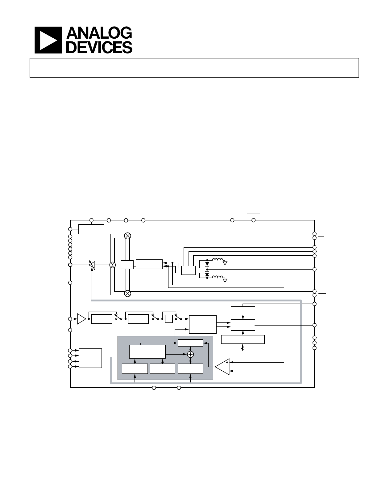
FUNCTIONAL BLOCKDIAGRAM
CC1VCC2VCC3VCC4
300 MHz to 2310 MHz I/Q Modulator
GENERAL DESCRIPTION
The ADRF6755 is a highly integrated quadrature modulator,
frequency synthesizer, and programmable attenuator. The
device covers an operating frequency range from 300 MHz
to 2310 MHz for use in satellite, cellular and broadband
communications.
The ADRF6755 modulator includes a high modulus fractional-N
frequency synthesizer with integrated VCO, providing better
than 1 Hz frequency resolution, and a 47 dB digitally controlled
output attenuator with 1 dB steps.
Control of all the on-chip registers is through a user-selected
SPI interface or I2C interface. The device operates from a single
power supply ranging from 4.75 V to 5.25 V.
LOMON
LOMON
REGOUT
VREG1
VREG2
VREG3
VREG4
VREG5
VREG6
RFOUT
TXDIS
REFIN
REFIN
SDI/SDA
CLK/SCL
SDO
CS
3.3V
REGULATOR
47dB
GAIN CONTROL
RANGE
×2
DOUBLER
SPI/
I2C
INTERFACE
ADRF6755
RFDIVIDER
0°/90°
5-BIT
DIVIDER
THIRD-ORDER
FRACTIONAL
INTERPOLATOR
FRACTIONAL
REGISTER
÷2
MODULUS
25
2
AGND DGND
VCO
CORE
+
FREQUENCY
DETECTOR
–
N-COUNTER
INTEGER
REGISTER
Figure 1.
PHASE
REFERENCE
CHARGE
PUMP
CURRENT SETTING
CR9[7:4]
IBB
IBB
CCOMP1
CCOMP2
CCOMP3
VTUNE
QBB
QBB
RSET
CP
LF3
LF2
LDET
08201-001
Rev. PrD
Information furnished by Analog Devices is believed to be accurate and reliable. However, no
responsibility is assumed by Analog Devices for its use, nor for any infringements of patents or other
rights of third parties that may result from its use. Specifications subject to change without notice. No
license is granted by implication or otherwise under any patent or patent rights of Analog Devices.
Trademarks and registered trademarks are the property of their respective owners.
One Technology Way, P.O. Box 9106, Norwood, MA 02062-9106, U.S.A.
Tel: 781.329.4700 www.analog.com
Fax: 781.461.3113 ©2012 Analog Devices, Inc. All rights reserved.

ADRF6755
TABLE OF CONTENTS
Features .............................................................................................. 1
General Description ......................................................................... 1
Functional Block Diagram .............................................................. 1
Specifications ..................................................................................... 3
Timing Characteristics ................................................................ 5
Absolute Maximum Ratings ............................................................ 7
ESD Caution .................................................................................. 7
Pin Configuration and Function Descriptions ............................. 8
Typical Performance Characteristics ........................................... 10
Theory of Operation ...................................................................... 18
Overview...................................................................................... 18
Preliminary Technical Data
SPI Interface ................................................................................ 24
Program Modes .......................................................................... 26
Register Map ................................................................................... 28
Register Map Summary ............................................................. 28
Register Bit Descriptions ........................................................... 29
Suggested Power-Up Sequence ..................................................... 33
Initial Register Write Sequence ................................................ 33
Evaluation Board ............................................................................ 35
General Description ................................................................... 35
Hardware Description ............................................................... 35
PCB Artwork .............................................................................. 38
PLL Synthesizer and VCO ......................................................... 18
Quadrature Modulator .............................................................. 21
Attenuator .................................................................................... 22
Voltage Regulator ....................................................................... 22
I2C Interface ................................................................................ 22
Bill of Materials........................................................................... 41
Outline Dimensions ....................................................................... 42
Ordering Guide .......................................................................... 42
Rev. PrD | Page 2 of 43

Preliminary Technical Data ADRF6755
SPECIFICATIONS
VCC = 5 V, TA = 25°C, I/Q inputs = 0.9 V p-p differential sine waves in quadrature on a 500 mV dc bias, REFIN = 80 MHz, PFD = 40 MHz,
baseband frequency = 1 MHz, LOMON off, unless otherwise noted.
Table 1.
Parameter Test Conditions/Comments Min Typ Max Unit
RF OUTPUT RFOUT pin
Operating Frequency Range 300 2310 MHz
Nominal Output Power VIQ = 0.9 V p-p differential −0.5 dBm
Gain Flatness Any 40 MHz ±0.1 dB
Output P1dB 8 dBm
Output IP3 f1BB = 3.5 MHz, f2BB = 4.5 MHz, P
Output Return Loss Attenuator setting = 0 dB −15 dB
LO Carrier Feedthrough Attenuator setting = 0 dB to 47 dB −45 dBc
2× LO Carrier Feedthrough Attenuator setting = 0 dB to 47 dB −45 dBm
Sideband Suppression −45 dBc
Noise Floor I/Q inputs = 0 V p-p differential, Attenuator setting = 0 dB −162 dBm/Hz
Attenuator setting = 0 dB to 21 dB, carrier offset = 15 MHz −147 dBc/Hz
Attenuator setting = 21 dB to 47 dB, carrier offset = 15 MHz −170 dBm/Hz
Harmonics −55 dBc
REFERENCE CHARACTERISTICS REFIN pin
Input Frequency With R divide-by-2 enabled 10 300 MHz
With R divide-by-2 disabled 10 165 MHz
Input Sensitivity AC-coupled 0.4 VREG V p-p
Input Capacitance 10 pF
Input Current ±100 µA
CHARGE PUMP
ICP Sink/Source Programmable, RSET = 4.7 kΩ
High Value 5 mA
Low Value 312.5 µA
Absolute Accuracy 4.0 %
VCO
Gain K
SYNTHESIZER SPECIFICATIONS
Frequency Resolution 1 Hz
Spurs Integer boundary < loop bandwidth −55 dBc
> 256 kHz offset from carrier −65 dBc
>10 MHz offset from carrier −75 dBc
Phase Noise1 LO = 2310 MHz
100 Hz offset −85 dBc/Hz
1 kHz offset −96 dBc/Hz
10 kHz offset −100 dBc/Hz
100 kHz offset −106 dBc/Hz
1 MHz offset −132 dBc/Hz
>15 MHz offset −152 dBc/Hz
Integrated Phase Noise1 1 kHz to 8 MHz integration bandwidth, LO=2310MHz 0.20
Frequency Settling1 Any step size, maximum frequency error = 100 Hz 0.17 ms
Maximum Frequency Step for
No Autocalibration
Phase Detector Frequency 10 40 MHz
25 MHz/V
VCO
Frequency step with no autocalibration routine;
Register CR24, Bit 0 = 1
= −6 dBm per tone 21 dBm
OUT
100/2
RFDIV
kHz
rms
Rev. PrD | Page 3 of 43

ADRF6755
INH
INH
INL
Preliminary Technical Data
Parameter Test Conditions/Comments Min Typ Max Unit
GAIN CONTROL
Gain Range 47 dB
Step Size 1 dB
Relative Step Accuracy Fixed frequency, adjacent steps
All attenuation steps ±0.3 dB
Over full frequency range, adjacent steps ±1.5 dB
Absolute Step Accuracy2 47 dB attenuation step −2.0 dB
Output Settling Time Any step; output power settled to ±0.2 dB 15 µs
OUTPUT DISABLE TXDIS pin
Off Isolation RFOUT, Attenuator setting = 0 dB to 47 dB, TXDIS high −100 dBm
LO, Attenuator setting = 0 dB to 47 dB, TXDIS high −80 dBm
2 x LO, Attenuator setting = 0 dB to 47 dB, TXDIS high −50 dBm
Turn-On Settling Time TXDIS high to low: Output power to 90% of envelope 500 ns
Frequency settling to 100Hz 2 µs
Turn-Off Settling Time TXDIS low to high (to −55 dBm) 500 ns
MONITOR OUTPUT
LOMON,
LOMON
pins,
Nominal Output Power −24 dBm
BASEBAND INPUTS
IBB
, QBB,
QBB
pins
IBB,
I and Q Input Bias Level 500 mV
3 dB Bandwidth 600 MHz
LOGIC INPUTS
Input High Voltage, V
Input Low Voltage, V
Input High Voltage, V
Input Low Voltage, V
Input Current, I
INH/IINL
CS, TXDIS pins 1.4 V
CS, TXDIS pins 0.6 V
INL
SDI/SDA, CLK/SCL pins 2.1 V
SDI/SDA, CLK/SCL pins 1.1 V
CS, TXDIS, SDI/SDA, CLK/SCL pins ±1 µA
Input Capacitance, CIN CS, TXDIS, SDI/SDA, CLK/SCL pins 10 pF
LOGIC OUTPUTS
Output High Voltage, VOH SDO, LDET pins; IOH = 500 µA 2.8 V
Output Low Voltage, VOL SDO, LDET pins; IOL = 500 µA 0.4 V
SDA (SDI/SDA); IOL = 3 mA 0.4 V
POWER SUPPLIES VCC1, VCC2, VCC3, VCC4, VREG1, VREG2, VREG3, VREG4,
VREG5, VREG6, and REGOUT pins
REGOUT normally connected to VREG1, VREG2, VREG3,
VREG4, VREG5, and VREG6
Voltage Range VCC1, VCC2, VCC3, and VCC4 4.75 5 5.25 V
REGOUT, VREG1, VREG2, VREG3, VREG4, VREG5, and
3.3 V
VREG6
Supply Current VCC1, VCC2, VCC3, and VCC4 combined; REGOUT con-
350 390 mA
nected to VREG1, VREG2, VREG3, VREG4, VREG5, and VREG6
Power Down Current CR29[0]=0, Power Down Modulator
7 mA
CR12[2]=1, Power Down PLL
CR28[4]=1, Power Down RFDIVIDER
CR27[2]=0, Power Down LOMON
Operating Temperature −40 85 °C
1
LBW = 100 kHz at LO = 2310 MHz; ICP = 5 mA.
2
All other attenuation steps have an absolute error of <±2.0 dB.
Rev. PrD | Page 4 of 43
Preliminary Technical Data ADRF6755
SC
L
LOW
HD;STA
SU;DAT
SU;
STO
VD;DAT
BUF
08201-003
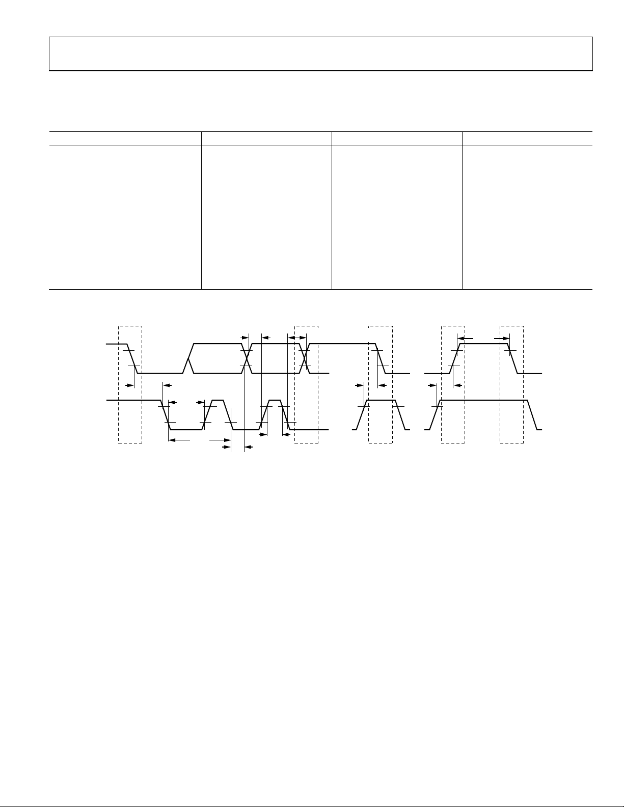
TIMING CHARACTERISTICS
I2C Interface Timing
Table 2.
Parameter1 Symbol Limit Unit
SCL Clock Frequency f
SCL Pulse Width High t
SCL Pulse Width Low t
Start Condition Hold Time t
Start Condition Setup Time t
Data Setup Time t
Data Hold Time t
Stop Condition Setup Time t
Data Valid Time t
Data Valid Acknowledge Time t
Bus Free Time t
1
See Figure 2.
400 kHz max
600 ns min
HIGH
1300 ns min
600 ns min
600 ns min
SU;STA
100 ns min
300 ns min
HD;DAT
600 ns min
900 ns max
900 ns max
VD;ACK
1300 ns min
t
t
SU;DAT
VD;DAT AND
t
VD;ACK (ACK SIGNAL ONLY)
t
BUF
SDA
SCL
t
HD;STA
t
LOW
S S SP
START
CONDITION
1/f
SCL
t
HD;DAT
t
HIGH
t
SU;STA
t
SU;STO
Figure 2. I2C Port Timing Diagram
STOP
CONDITION
Rev. PrD | Page 5 of 43
ADRF6755
t
Preliminary Technical Data
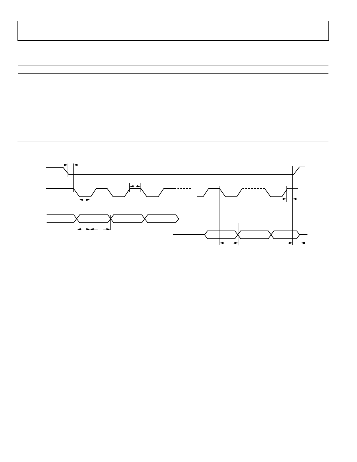
SPI Interface Timing
Table 3.
Parameter1 Symbol Limit Unit
CLK Frequency f
20 MHz max
CLK
CLK Pulse Width High t1 15 ns min
CLK Pulse Width Low t2 15 ns min
Start Condition Hold Time t3 5 ns min
Data Setup Time t4 10 ns min
Data Hold Time t5 5 ns min
Stop Condition Setup Time t6 5 ns min
SDO Access Time t7 15 ns min
CS to SDO High Impedance t8 25 ns max
1
See Figure 3.
3
CS
t
1
CLK
SDI
t
t
2
t
t
5
4
Figure 3. SPI Port Timing Diagram
SDO
t
7
6
t
8
08201-004
Rev. PrD | Page 6 of 43
Preliminary Technical Data ADRF6755
ABSOLUTE MAXIMUM RATINGS
Table 4.
Parameter Rating
Supply Voltage VCC1, VCC2, VCC3, and VCC4 −0.3 V to +6 V
Supply Voltage VREG1, VREG2, VREG3, VREG4,
VREG5, and VREG6
IBB,
, QBB, and
IBB
Digital I/O −0.3 V to +4 V
Analog I/O (Other Than IBB,
)
QBB
Maximum Junction Temperature 125°C
Storage Temperature Range −65°C to +150°C
QBB
, QBB, and
IBB
−0.3 V to +4 V
0 V to 2.5 V
−0.3 V to +4 V
Stresses above those listed under Absolute Maximum Ratings
may cause permanent damage to the device. This is a stress
rating only; functional operation of the device at these or any
other conditions above those indicated in the operational
section of this specification is not implied. Exposure to absolute
maximum rating conditions for extended periods may affect
device reliability.
ESD CAUTION
Rev. PrD | Page 7 of 43
Preliminary Technical Data ADRF6755
SET
T
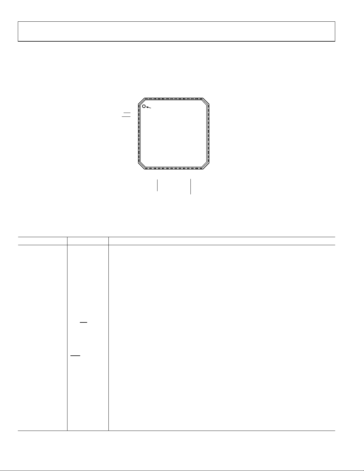
PIN CONFIGURATION AND FUNCTION DESCRIPTIONS
D
2
2
N
N
C
C
G
G
C
C
A
A
V
V
3
4
5
6
5
5
5
5
PIN 1
1VCC4
INDICATOR
2IBB
3IBB
4QBB
5QBB
6AGND
7RSET
8LF3
9CP
10LF2
11VCC1
12REGOUT
13VREG1
14VREG2
NOTES
1. CONNECT EXPOSED PAD TO GROUND PLANE VIA
A LOW IMPEDANCE PATH.
6
7
5
1
1
1
3
4
N
I
G
G
F
E
E
E
R
R
R
V
V
ADRF6755
TOP VIEW
(Not to Scale)
8
1
N
I
F
E
R
U
N
N
N
N
O
F
G
G
G
G
R
A
A
A
A
2
8
9
0
1
5
4
4
5
5
1
9
0
2
1
2
22232
D
D
D
D
D
N
N
N
N
N
G
G
G
G
G
A
A
A
A
A
T
D
D
D
D
D
U
S
D
D
O
I
T
X
N
N
E
D
U
G
G
X
D
T
A
A
L
M
4
3
5
6
7
4
4
4
4
4
42 VCC3
41 VCC3
40 AGND
39 AGND
38 VTUNE
37 AGND
36 VREG6
35 CCOMP3
34 CCOMP2
33 CCOMP1
32 DGND
31 VREG5
30 CLK/SCL
29 SDI/SDA
4
5
6
7
8
2
2
2
2
S
D
N
N
O
C
N
O
D
O
S
G
M
M
A
O
O
L
L
08298-005
Figure 4. Pin Configuration
Table 5. Pin Function Descriptions
Pin No. Mnemonic Description
11, 55, 56, 41, 42, 1 VCC1 to VCC4 Positive Power Supplies for I/Q Modulator. Apply a 5 V power supply to VCC1, which should be
decoupled with power supply decoupling capacitors. Connect VCC2, VCC3, and VCC4 to the same
5 V power supply.
12 REGOUT 3.3 V Output Supply. Drives VREG1, VREG2, VREG3, VREG4, VREG5, and VREG6.
13, 14, 15, 16, 31,
36
6, 19, 20, 21, 22, 23,
VREG1 to
VREG6
Positive Power Supplies for PLL Synthesizer, VCO, and Serial Port. Connect these pins to REGOUT
(3.3 V) and decouple them separately.
AGND Analog Ground. Connect to a low impedance ground plane.
24, 37, 39, 40, 46,
47, 49, 50, 51, 52,
53, 54
32 DGND Digital Ground. Connect to the same low impedance ground plane as the AGND pins.
IBB,
2, 3
IBB
Differential In-Phase Baseband Inputs. These high impedance inputs must be dc-biased to approximately 500 mV dc and should be driven from a low impedance source. Nominal characterized ac
signal swing is 450 mV p-p on each pin. This results in a differential drive of 0.9 V p-p with a 500 mV
dc bias, resulting in a single sideband output power of approximately −1.6 dBm. These inputs are
not self-biased and must be externally biased.
4, 5
QBB
, QBB
Differential Quadrature Baseband Inputs. These high impedance inputs must be dc-biased to
approximately 500 mV dc and should be driven from a low impedance source. Nominal characterized ac signal swing is 450 mV p-p on each pin. This results in a differential drive of 0.9 V p-p with
a 500 mV dc bias, resulting in a single sideband output power of approximately −1.6 dBm. These
inputs are not self-biased and must be externally biased.
33, 34, 35 CCOMP1 to
Internal Compensation Nodes. These pins must be decoupled to ground with a 100 nF capacitor.
CCOMP3
38 VTUNE Control Input to the VCO. This voltage determines the output frequency and is derived from
filtering the CP output voltage.
7 RSET Charge Pump Current Set. Connecting a resistor between this pin and ground sets the maximum
charge pump output current. The relationship between ICP and R
is as follows:
Rev. PrD | Page 8 of 43

Preliminary Technical Data ADRF6755
SET
CP max
Pin No. Mnemonic Description
5.23
I
CPmax
where R
9 CP Charge Pump Output. When enabled, this output provides ±ICP to the external loop filter, which, in
turn, drives the internal VCO.
27 CS Chip Select, CMOS Input. When CS is high, the data stored in the shift registers is loaded into one of
31 latches. In I2C mode, when CS is high, the slave address of the device is 0x60, and when CS is low,
the slave address is 0x40.
29 SDI/SDA Serial Data Input for SPI Port/Serial Data Input/Output for I2C Port. In SPI mode, this pin is a high
impedance CMOS data input, and data is loaded in an 8-bit word. In I2C mode, this pin is a bidirectional port.
30 CLK/SCL Serial Clock Input for SPI/I2C Port. This serial clock is used to clock in the serial data to the registers.
This input is a high impedance CMOS input.
28 SDO Serial Data Output for SPI Port. Register states can be read back on the SDO data output line.
17 REFIN Reference Input. This high impedance CMOS input should be ac-coupled.
18
REFIN
Reference Input Bar. This pin should be either grounded or ac-coupled to ground.
48 RFOUT RF Output. Single-ended, 50 Ω, internally biased RF output. This pin must be ac-coupled to the
load. Nominal output power is −1.6 dBm for a single sideband baseband drive of 0.9 V p-p differ-
ential on the I and Q inputs (attenuation = minimum).
45 TXDIS Output Disable. This pin can be used to disable the RF output. Connect to high logic level to disable
the output. Connect to low logic level for normal operation.
25, 26 LOMON,
LOMON
Differential Monitor Outputs. These pins provide a replica of the internal local oscillator frequency
(1× LO) at four different power levels: −6 dBm, −12 dBm, −18 dBm, and −24 dBm, approximately.
These open-collector outputs must be terminated with external resistors to REGOUT. These outputs
can be disabled through serial port programming and should be tied to REGOUT if not used.
10, 8 LF2, LF3 No connect pins.
44 LDET Lock Detect. This output pin indicates the state of the PLL: a high level indicates a locked condition,
whereas a low level indicates a loss of lock condition.
43 MUXOUT Muxout. This output is a test output for diagnostic use only. It should be left unconnected by the
customer.
Exposed Paddle EP Exposed Paddle. Connect to ground plane via a low impedance path.
R
SET
= 4.7 kΩ and I
= 5 mA.
Rev. PrD | Page 9 of 43

Preliminary Technical Data ADRF6755
odata
vailabl
e
odatavailable
odatavailable
odatavailableodatavailabl
e
odatavailable
TYPICAL PERFORMANCE CHARACTERISTICS
VCC = 5 V, TA = 25°C, I/Q inputs = 0.9 V p-p differential sine waves in quadrature on a 500 mV dc bias, REFIN = 80 MHz, PFD = 40 MHz,
baseband frequency = 1 MHz, LOMON is off, unless otherwise noted. A nominal condition is defined as 25°C, 5.00 V, and worst-case
frequency. A worst-case condition is defined as having the worst-case temperature, supply voltage, and frequency.
Figure 5. Output Power vs. LO Frequency, Supply, and Temperature
Figure 6. Output Power Distribution at Nominal and
Worst-Case Conditions
Figure 8. Sideband Suppression vs. LO Frequency, Supply, and Temperature
Figure 9. Sideband Suppression Distribution at Nominal and
Worst-Case Conditions
Figure 7. Output Power vs. LO Frequency for External VCO Mode
at Nominal Conditions
Figure 10. LO Carrier Feedthrough vs. Attenuation, LO Frequency,
Supply, and Temperature
Rev. PrD | Page 10 of 43

Preliminary Technical Data ADRF6755
odatavailable
odata
vailabl
e
odata
vailabl
e
odata
vailabl
e
odatavailable
odata
vailabl
e
Figure 11. LO Carrier Feedthrough Distribution at Nominal and Worst-Case
Conditions and Attenuation Setting
Figure 12. 2 × LO Carrier Feedthrough vs. Attenuation, LO Frequency,
Supply, and Temperature
Figure 14. Output P1dB Compression Point Distribution at Nominal
and Worst-Case Conditions
Figure 15. Output P1dB Compression Point vs. LO Frequency at
Nominal Conditions
Figure 13. Output P1dB Compression Point at Worst-Case LO Frequency
vs. Supply and Temperature
Rev. PrD | Page 11 of 43
Figure 16. Output IP3 Distribution at Nominal and Worst-Case
Conditions

ADRF6755
odatavailable
odatavailable
odata
vailabl
e
odata
vailabl
e
odatavailable
odata
vailabl
e
Preliminary Technical Data
Figure 17. Output IP3 vs. LO Frequency at Nominal Conditions
Figure 18. LO Off Isolation vs. Attenuation, LO Frequency, Supply,
and Temperature
Figure 20. Second-Order and Third-Order Harmonic Distortion vs.
Figure 21. Noise Floor at 15 MHz Offset Frequency Distribution at
LO Frequency, Supply, and Temperature
Worst-Case Conditions and Different Attenuation Settings
Figure 19. 2 × LO Off Isolation vs. Attenuation, LO Frequency, Supply,
and Temperature
Figure 22. Noise Floor at 0 dB Attenuation vs. Output Power
at Nominal Conditions
Rev. PrD | Page 12 of 43

Preliminary Technical Data ADRF6755
odata
vailabl
e
odata
vailabl
e
odata
vailabl
e
odatavailable
odatavailable
odata
vailabl
e
Figure 23. Normalized I and Q Input Bandwidth
Figure 24. Output Return Loss at Worst-Case Attenuation vs.
LO Frequency, Supply, and Temperature
Figure 26. RF Output Spectral Plot over a 100 MHz Span
Figure 27. RF Output Spectral Plot over a Wide Span
Figure 25. RF Output Spectral Plot over a 10 MHz Span
Rev. PrD | Page 13 of 43
Figure 28. Phase Noise Performance vs. LO Frequency, Supply,
and Temperature
 Loading...