

1200 MHz to 2400 MHz Quadrature Modulator with
V
V
V
V
V
V
V
1550 MHz to 2150 MHz Frac-N PLL and Integrated VCO
Data Sheet
FEATURES
IQ modulator with integrated fractional-N PLL
Output frequency range: 1200 MHz to 2400 MHz
Internal LO frequency range: 1550 MHz to 2150 MHz
Output P1dB: 13.1 dBm @ 2140 MHz
Output IP3: 29.1 dBm @ 2140 MHz
Noise floor: −159.6 dBm/Hz @ 1960 MHz
Baseband bandwidth: 750 MHz (3 dB)
SPI serial interface for PLL programming
Integrated LDOs and LO buffer
Power supply: 5 V/240 mA
40-lead 6 mm × 6 mm LFCSP
APPLICATIONS
Cellular communications systems
GSM/EDGE, CDMA2000, W-CDMA, TD-SCDMA, LTE
Broadband wireless access systems
Satellite modems
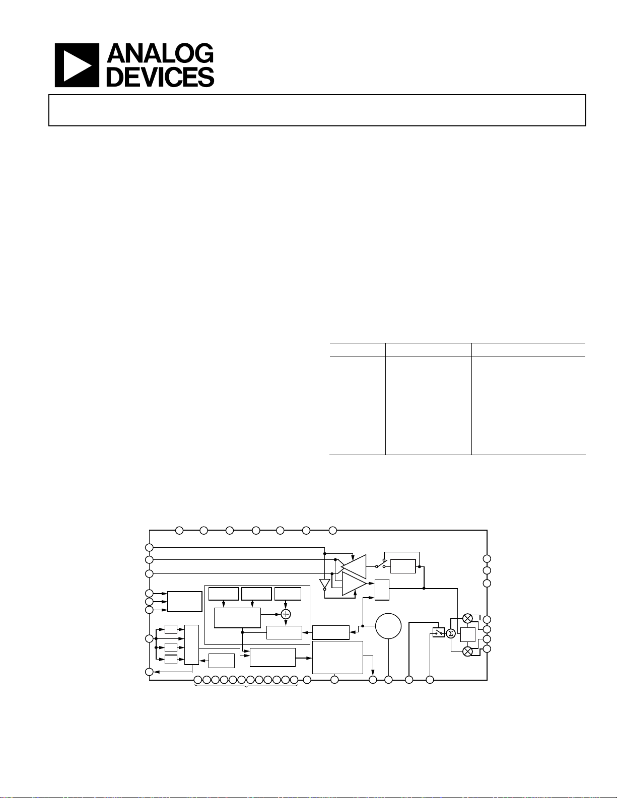
GENERAL DESCRIPTION
The ADRF6702 provides a quadrature modulator and
synthesizer solution within a small 6 mm × 6 mm footprint
while requiring minimal external components.
The ADRF6702 is designed for RF outputs from 1200 MHz to
2400 MHz. The low phase noise VCO and high performance
quadrature modulator make the ADRF6702 suitable for next
generation communication systems requiring high signal
dynamic range and linearity. The integration of the IQ
modulator, PLL, and VCO provides for significant board
savings and reduces the BOM and design complexity.
ADRF6702
The integrated fractional-N PLL/synthesizer generates a 2× f
input to the IQ modulator. The phase detector together with an
external loop filter is used to control the VCO output. The VCO
output is applied to a quadrature divider. To reduce spurious
components, a sigma-delta (Σ-) modulator controls the
programmable PLL divider.
The IQ modulator has wideband differential I and Q inputs,
which support baseband as well as complex IF architectures.
The single-ended modulator output is designed to drive a
50 Ω load impedance and can be disabled.
The ADRF6702 is fabricated using an advanced silicongermanium BiCMOS process. It is available in a 40-lead,
exposed-paddle, Pb-free, 6 mm × 6 mm LFCSP package.
Performance is specified from −40°C to +85°C. A lead-free
evaluation board is available.
Table 1.
Part No. Internal LO Range ±3 dB RF
Balun Range
OUT
ADRF6701 750 MHz 400 MHz
1150 MHz 1250 MHz
ADRF6702 1550 MHz 1200 MHz
2150 MHz 2400 MHz
ADRF6703 2100 MHz 1550 MHz
2600 MHz 2650 MHz
ADRF6704 2500 MHz 2050 MHz
290 MHz 3000 MHz
LO
FUNCTIONAL BLOCK DIAGRAM
CC5
CC6
CC7
29
34
36
LOSEL
LON
37
38
LOP
12
DATA
13
CLK
14
LE
6
REFIN
8
MUXOUT
NOTES
1. NC = NO CONNECT. DO NOT CO NNECT TO THIS PI N.
Rev. B
Information furnished by Analog Devices is believed to be accurate and reliable. However, no
responsibility is assumed by Anal og Devices for its use, nor for any infringements of patents or ot her
rights of third parties that may result from its use. Specifications subject to change without notice. No
license is granted by implication or otherwise under any patent or patent rights of Analog Devices.
Trademarks and registered trademarks are the property of their respective owners.
SPI
INTERFACE
×2
MUX
÷2
÷4
27 17 10 122
FRACTION
SENSOR
7 11 15 20 21 23 2425 28 30 31 35
MODULUS
REG
THIRD-ORDER
FRACTIONAL
INTERPOL ATOR
TEMP
GND
CC4
N COUNTER
–
PHASE
+
FREQUENCY
DETECTOR
CC3
INTEGER
REG
21 TO 123
CC1
CC2
PRESCALER
÷2
CHARGE PUMP
250µA,
500µA (DEFAULT ),
750µA,
1000µA
RSET CP VTUNE
Figure 1.
One Technology Way, P.O. Box 9106, Norwood, MA 02062-9106, U.S.A.
Tel: 781.329.4700 www.analog.com
Fax: 781.461.3113 ©2011 Analog Devices, Inc. All rights reserved.
BUFFER
BUFFER
2:1
MUX
VCO
CORE
DIVIDER
÷2
ENOP
ADRF6702
261639354
RFOUTNC
0/90
40
DECL3
9
DECL2
2
DECL1
18
QP
19
QN
÷2
32
IN
33
IP
08568-001

ADRF6702 Data Sheet
TABLE OF CONTENTS
Features.............................................................................................. 1
Applications....................................................................................... 1
General Description ......................................................................... 1
Functional Block Diagram .............................................................. 1
Revision History ............................................................................... 2
Specifications..................................................................................... 3
Timing Characteristics ................................................................ 6
Absolute Maximum Ratings............................................................ 7
ESD Caution.................................................................................. 7
Pin Configuration and Function Descriptions............................. 8
Typical Performance Characteristics ........................................... 10
Theory of Operation ...................................................................... 16
PLL + VCO.................................................................................. 16
Basic Connections for Operation............................................. 16
External LO ................................................................................. 16
Loop Filter ................................................................................... 17
DAC-to-IQ Modulator Interfacing ..........................................18
Adding a Swing-Limiting Resistor ........................................... 18
IQ Filtering.................................................................................. 19
Baseband Bandwidth ................................................................. 19
Device Programming and Register Sequencing..................... 19
Register Summary .......................................................................... 20
Register Description....................................................................... 21
Register 0—Integer Divide Control (Default: 0x0001C0) .... 21
Register 1—Modulus Divide Control (Default: 0x003001).. 22
Register 2—Fractional Divide Control (Default: 0x001802) 22
Register 3—Σ- Modulator Dither Control (Default:
0x10000B).................................................................................... 23
Register 4—PLL Charge Pump, PFD, and Reference Path
Control (Default: 0x0AA7E4)................................................... 24
Register 5—LO Path and Modulator Control (Default:
0x0000D5)................................................................................... 26
Register 6—VCO Control and VCO Enable (Default:
0x1E2106).................................................................................... 27
Register 7—External VCO Enable........................................... 27
Characterization Setups................................................................. 28
Evaluation Board............................................................................ 30
Evaluation Board Control Software......................................... 30
Outline Dimensions....................................................................... 35
Ordering Guide .......................................................................... 35
REVISION HISTORY
10/11—Rev. A to Rev. B
Changes Table 1 ................................................................................ 1
7/11—Rev. 0 to Rev. A
Changes to Noise Floor in Features Section and Table 1 ............ 1
Changes to Specifications Section.................................................. 2
Changes to Figure 16, Figure 17, and Figure 18 ......................... 12
Changes to Figure 28...................................................................... 14
Changes to Figure 32 and Figure 34............................................. 15
Added Figure 34, Renumbered Sequentially .............................. 15
Changes to Figure 35...................................................................... 17
Added Figure 40.............................................................................. 19
Changes to Figure 52...................................................................... 31
4/11—Revision 0: Initial Version
Rev. B | Page 2 of 36

Data Sheet ADRF6702
SPECIFICATIONS
VS = 5 V; TA = 25°C; baseband I/Q amplitude = 1 V p-p differential sine waves in quadrature with a 500 mV dc bias; baseband I/Q
frequency (f
Table 2.
Parameter Test Conditions/Comments Min Typ Max Unit
OPERATING FREQUENCY RANGE IQ modulator (±3 dB RF output range) 1200 2400 MHz
PLL LO range 1550 2150 MHz
RF OUTPUT = 1850 MHz RFOUT pin
Nominal Output Power Baseband VIQ = 1 V p-p differential 4 dBm
IQ Modulator Voltage Gain RF output divided by baseband input voltage 0 dB
OP1dB 13.5 dBm
Carrier Feedthrough −41.2 dBm
Sideband Suppression −43.7 dBc
Quadrature Error ±1 Degrees
I/Q Amplitude Balance 0.02 dB
Second Harmonic P
Third Harmonic P
Output IP2 f1BB = 3.5 MHz, f2BB = 4.5 MHz, P
Output IP3 f1BB = 3.5 MHz, f2BB = 4.5 MHz, P
Noise Floor I/Q inputs = 0 V differential with 500 mV dc bias, 20 MHz carrier offset −158.9 dBm/Hz
RF OUTPUT = 1960 MHz RFOUT pin
Nominal Output Power Baseband VIQ = 1 V p-p differential 4.1 dBm
IQ Modulator Voltage Gain RF output divided by baseband input voltage 0.1 dB
OP1dB 13.6 dBm
Carrier Feedthrough −40.6 dBm
Sideband Suppression −53.9 dBc
Quadrature Error +0.7/−1.7 Degrees
I/Q Amplitude Balance 0.03 dB
Second Harmonic P
Third Harmonic P
Output IP2 f1BB = 3.5 MHz, f2BB = 4.5 MHz, P
Output IP3 f1BB = 3.5 MHz, f2BB = 4.5 MHz, P
Noise Floor I/Q inputs = 0 V differential with 500 mV dc bias, 20 MHz carrier offset −159.6 dBm/Hz
RF OUTPUT = 2140 MHz RFOUT pin
Nominal Output Power Baseband VIQ = 1 V p-p differential 3.8 dBm
IQ Modulator Voltage Gain RF output divided by baseband input voltage −0.2 dB
OP1dB 13.1 dBm
Carrier Feedthrough −46.8 dBm
Sideband Suppression −44.4 dBc
Quadrature Error ±1 Degrees
I/Q Amplitude Balance 0.02 dB
Second Harmonic P
Third Harmonic P
Output IP2 f1BB = 3.5 MHz, f2BB = 4.5 MHz, P
Output IP3 f1BB = 3.5 MHz, f2BB = 4.5 MHz, P
Noise Floor I/Q inputs = 0 V differential with 500 mV dc bias, 20 MHz carrier offset −158.1 dBm/Hz
SYNTHESIZER SPECIFICATIONS Synthesizer specifications referenced to the modulator output
Internal LO Range 1550 2150 MHz
Figure of Merit (FOM)1 −220.5 dBc/Hz/Hz
) = 1 MHz; f
BB
= 38.4 MHz; f
PFD
OUT
OUT
OUT
OUT
OUT
OUT
= 153.6 MHz at +4 dBm Re:50 (1 V p-p); 130 kHz loop filter, unless otherwise noted.
REF
− P (fLO ± (2 × fBB)) −62.2 dBc
− P (fLO ± (3 × fBB)) −50.6 dBc
≈ −2 dBm per tone 56 dBm
OUT
≈ −2 dBm per tone 31 dBm
OUT
− P (fLO ± (2 × fBB)) −74.6 dBc
− P (fLO ± (3 × fBB)) −54.1 dBc
≈ −2 dBm per tone 66.4 dBm
OUT
≈ −2 dBm per tone 30.1 dBm
OUT
− P (fLO ± (2 × fBB)) −71.8 dBc
− P (fLO ± (3 × fBB)) −57.3 dBc
≈ −2 dBm per tone 70.4 dBm
OUT
≈ −2 dBm per tone) 29.1 dBm
OUT
Rev. B | Page 3 of 36

ADRF6702 Data Sheet
Parameter Test Conditions/Comments Min Typ Max Unit
REFERENCE CHARACTERISTICS REFIN, MUXOUT pins
REFIN Input Frequency 12 160 MHz
REFIN Input Capacitance 4 pF
Phase Detector Frequency 20 40 MHz
MUXOUT Output Level Low (lock detect output selected) 0.25 V
High (lock detect output selected) 2.7 V
MUXOUT Duty Cycle 50 %
CHARGE PUMP
Charge Pump Current Programmable to 250 µA, 500 µA, 750 µA, 1000 µA 500 µA
Output Compliance Range 1 2.8 V
PHASE NOISE (FREQUENCY =
1850 MHz, f
= 38.4 MHz)
PFD
Closed loop operation (see
Figure 35 for loop filter design)
10 kHz offset −110.8 dBc/Hz
100 kHz offset −105.8 dBc/Hz
1 MHz offset −124.6 dBc/Hz
10 MHz offset −150 dBc/Hz
Integrated Phase Noise 1 kHz to 10 MHz integration bandwidth 0.27
Reference Spurs f
f
f
f
f
PHASE NOISE (FREQUENCY =
1960 MHz, f
= 38.4 MHz)
PFD
/2 −112 dBc
PFD
−84 dBc
PFD
× 2 −87 dBc
PFD
× 3 −93 dBc
PFD
× 4 −90 dBc
PFD
Closed loop operation (see Figure 35 for loop filter design)
10 kHz offset −108.5 dBc/Hz
100 kHz offset −104.2 dBc/Hz
1 MHz offset −125.1 dBc/Hz
10 MHz offset −149.9 dBc/Hz
Integrated Phase Noise 1 kHz to 10 MHz integration bandwidth 0.25
Reference Spurs f
f
f
f
f
PHASE NOISE (FREQUENCY =
2140 MHz, f
= 38.4 MHz)
PFD
/2 −110 dBc
PFD
−83 dBc
PFD
× 2 −97 dBc
PFD
× 3 −91 dBc
PFD
× 4 −97 dBc
PFD
Closed loop operation (see Figure 35 for loop filter design)
10 kHz offset −107.5 dBc/Hz
100 kHz offset −102.7 dBc/Hz
1 MHz offset −126.1 dBc/Hz
10 MHz offset −150.4 dBc/Hz
Integrated Phase Noise 1 kHz to 10 MHz integration bandwidth 0.25
Reference Spurs f
f
f
f
f
/2 −111 dBc
PFD
−86 dBc
PFD
× 2 −88 dBc
PFD
× 3 −91 dBc
PFD
× 4 −99 dBc
PFD
RF OUTPUT HARMONICS Measured at RFOUT, frequency = 2140 MHz
Second harmonic −47 dBc
Third harmonic −74 dBc
LO INPUT/OUTPUT LOP, LON
Output Frequency Range Divide by 2 circuit in LO path enabled 1550 2150 MHz
Divide by 2 circuit in LO path disabled 3100 4300 MHz
LO Output Level at 1960 MHz 2× LO or 1× LO mode, into a 50 Ω load, LO buffer enabled 1 dBm
LO Input Level Externally applied 2× LO, PLL disabled 0 dBm
LO Input Impedance Externally applied 2× LO, PLL disabled 50 Ω
Rev. B | Page 4 of 36
°rms
°rms
°rms

Data Sheet ADRF6702
Parameter Test Conditions/Comments Min Typ Max Unit
BASEBAND INPUTS IP, IN, QP, QN pins
I and Q Input DC Bias Level 400 500 600 mV
Bandwidth P
0.5 dB 350 MHz
3 dB 750 MHz
Differential Input Impedance 920 Ω
Differential Input Capacitance 1 pF
LOGIC INPUTS CLK, DATA, LE, ENOP, LOSEL
Input High Voltage, V
Input Low Voltage, V
Input Current, I
1.4 3.3 V
INH
0 0.7 V
INL
0.1 µA
INH/IINL
Input Capacitance, CIN 5 pF
TEMPERATURE SENSOR VPTAT voltage measured at MUXOUT
Output Voltage
Temperature Coefficient
POWER SUPPLIES VCC1, VCC2, VCC3, VCC4, VCC5, VCC6, VCC7
Voltage Range 4.75 5 5.25 V
Supply Current Normal Tx mode (PLL and IQMOD enabled, LO buffer disabled) 240 mA
Tx mode using external LO input (internal VCO/PLL disabled) 130 mA
Tx mode with LO buffer enabled 290 mA
Power-down mode 22 µA
1
The figure of merit (FOM) is computed as phase noise (dBc/Hz) – 10log10(f
f
power = 10 dBm (500 V/s slew rate) with a 40 MHz f
REF
≈ −7 dBm, RF flatness of IQ modulator output calibrated out
OUT
= 25°C, RL ≥10 kΩ (LO buffer disabled)
T
A
= −40°C to +85°C, RL ≥10 kΩ
T
A
) – 20log10(fLO/f
. The FOM was computed at 50 kHz offset.
PFD
PFD
). The FOM was measured across the full LO range, with f
PFD
1.64 V
3.9
mV/°C
= 80 MHz,
REF
Rev. B | Page 5 of 36
ADRF6702 Data Sheet
A
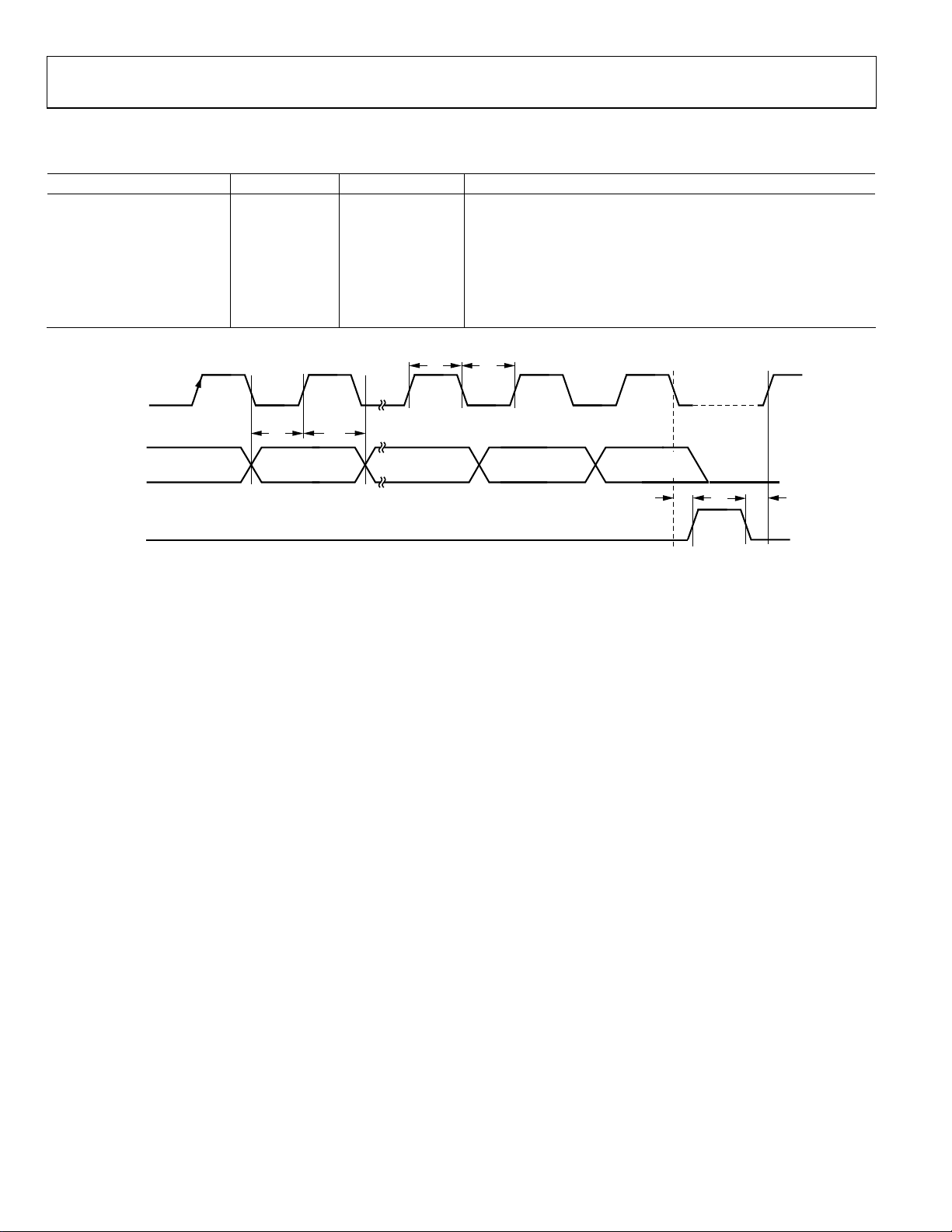
TIMING CHARACTERISTICS
Table 3.
Parameter Limit Unit Test Conditions/Comments
t1 20 ns min LE to CLK setup time
t2 10 ns min DATA to CLK setup time
t3 10 ns min DATA to CLK hold time
t4 25 ns min CLK high duration
t5 25 ns min CLK low duration
t6 10 ns min CLK to LE setup time
t7 20 ns min LE pulse width
CLK
t
4
t
5
t
2
D
DB23 (MSB) DB 22
TA
LE
t
3
DB2 DB1
(CONTROL BIT C2)(CONTROL BIT C3)
DB0 (LSB)
(CONTROL BIT C1)
t
t
t
7
6
1
08568-002
Figure 2. Timing Diagram
Rev. B | Page 6 of 36
Data Sheet ADRF6702
ABSOLUTE MAXIMUM RATINGS
Table 4.
Parameter Rating
Supply Voltage (VCC1 to VCC7) 5.5 V
Digital I/O, CLK, DATA, LE −0.3 V to +3.6 V
LOP, LON 18 dBm
IP, IN, QP, QN −0.5 V to +1.5 V
REFIN −0.3 V to +3.6 V
θJA (Exposed Paddle Soldered Down)1 35°C/W
Maximum Junction Temperature 150°C
Operating Temperature Range −40°C to +85°C
Storage Temperature Range −65°C to +150°C
1
Per JDEC standard JESD 51-2.
Stresses above those listed under Absolute Maximum Ratings
may cause permanent damage to the device. This is a stress
rating only; functional operation of the device at these or any
other conditions above those indicated in the operational
section of this specification is not implied. Exposure to absolute
maximum rating conditions for extended periods may affect
device reliability.
ESD CAUTION
Rev. B | Page 7 of 36
ADRF6702 Data Sheet
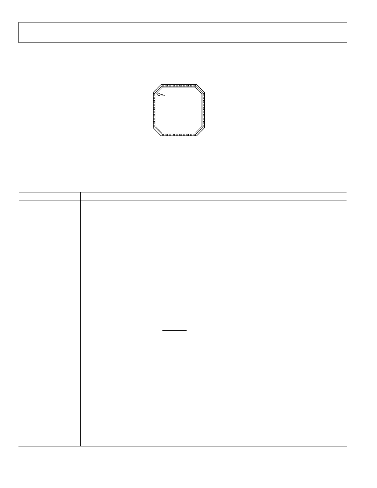
PIN CONFIGURATION AND FUNCTION DESCRIPTIONS
SEL
ND
CC7
IP
V
G
LO
LON
LOP
VTUNE
DECL3
37
38
39
40
PIN 1
1VCC1
INDICATOR
2DECL1
3CP
4
GND
RSET
REFIN
GND
MUXOUT
DECL2
10
VCC2
NOTES
1. NC = NO CONNECT. DO NOT CONNECT TO THIS PIN.
2. THE EXPOSED PADDLE SHOULD BE SOLDERED TO A
LOW IMPEDANCE GROUND PL ANE.
5
6
7
8
9
ADRF6702
TOP VIEW
(Not to Scale)
11
12
13
14
LE
CLK
GND
DATA
Figure 3. Pin Configuration
Table 5. Pin Function Descriptions
Pin No. Mnemonic Description
1, 10, 17, 22, 27, 29, 34
2 DECL1
VCC1, VCC2, VCC3,
VCC4, VCC5, VCC6,
VCC7
Power Supply Pins. The power supply voltage range is 4.75 V to 5.25 V. Drive all of
these pins from the same power supply voltage. Decouple each pin with 100 pF and
0.1 µF capacitors located close to the pin.
Decoupling Node for Internal 3.3 V LDO. Decouple this pin with 100 pF and 0.1 µF
capacitors located close to the pin.
3 CP
Charge Pump Output Pin. Connect VTUNE to this pin through the loop filter. If
an external VCO is being used, connect the output of the loop filter to the VCO’s
voltage control pin. The PLL control loop should then be closed by routing the VCO’s
frequency output back into the ADRF6702 through the LON and LOP pins.
4, 7, 11, 15, 20, 21, 23,
GND Ground. Connect these pins to a low impedance ground plane.
25, 28, 30, 31, 35
24 NC Do not connect to this pin.
5 RSET
Charge Pump Current. The nominal charge pump current can be set to 250 µA, 500 µA,
750 µA, or 1000 µA using DB10 and DB11 of Register 4 and by setting DB18 to 0 (CP
reference source).
In this mode, no external RSET is required. If DB18 is set to 1, the four nominal charge
pump currents (I
equation:
×
4.217
⎛
⎜
= 8.37
R
SET
⎜
I
NOMINAL
⎝
where I
is the base charge pump current in microamps. For further details on the
CP
charge pump current, see the Register 4—PLL Charge Pump, PFD, and Reference Path
Control section.
6 REFIN
Reference Input. The nominal input level is 1 V p-p. Input range is 12 MHz to 160 MHz.
This pin has high input impedance and should be ac-coupled. If REFIN is being driven
by laboratory test equipment, the pin should be externally terminated with a 50 Ω
resistor (place the ac-coupling capacitor between the pin and the resistor). When
driven from an 50 Ω RF signal generator, the recommended input level is 4 dBm.
8 MUXOUT
Multiplexer Output. This output allows a digital lock detect signal, a voltage
proportional to absolute temperature (VPTAT), or a buffered, frequency-scaled
reference signal to be accessed externally. The output is selected by programming
DB21 to DB23 in Register 4.
9 DECL2
Decoupling Node for 2.5 V LDO. Connect 100 pF, 0.1 µF, and 10 µF capacitors between this
pin and ground.
12 DATA
Serial Data Input. The serial data input is loaded MSB first with the three LSBs being
the control bits.
GND
IN
32
31
33
34
35
36
30 GND
29 VCC6
28 GND
27 VCC5
RFOUT
26
25
GND
24 NC
23 GND
22 VCC4
21
GND
15
17
16
20
19
18
QP
QN
GND
GND
VCC3
ENOP
08568-003
) can be externally tweaked according to the following
NOMINAL
I
⎞
CP
⎟
Ω−
⎟
⎠
Rev. B | Page 8 of 36
Data Sheet ADRF6702
Pin No. Mnemonic Description
13 CLK
14 LE
16 ENOP Modulator Output Enable/Disable. See Table 6.
18, 19, 32, 33 QP, QN, IN, IP
26 RFOUT
36 LOSEL
37, 38 LON, LOP
39 VTUNE
40 DECL3
EP
Serial Clock Input. This serial clock input is used to clock in the serial data to the
registers. The data is latched into the 24-bit shift register on the CLK rising edge.
Maximum clock frequency is 20 MHz.
Latch Enable. When the LE input pin goes high, the data stored in the shift registers is
loaded into one of the six registers, the relevant latch being selected by the first three
control bits of the 24-bit word.
Modulator Baseband Inputs. Differential in-phase and quadrature baseband inputs.
These inputs should be dc-biased to 0.5 V.
RF Output. Single-ended, 50 Ω internally biased RF output. RFOUT must be ac-coupled
to its load.
LO Select. This digital input pin determines whether the LOP and LON pins operate as
inputs or outputs. This pin should not be left floating. LOP and LON become inputs if
the LOSEL pin is set low and the LDRV bit of Register 5 is set low. External LO drive
must be a 2× LO. In addition to setting LOSEL and LDRV low and providing an external
2× LO, the LXL bit of Register 5 (DB4) must be set to 1 to direct the external LO to the
IQ modulator. LON and LOP become outputs when LOSEL is high or if the LDRV bit of
Register 5 (DB3) is set to 1. A 1× LO or 2× LO output can be selected by setting the
LDIV bit of Register 5 (DB5) to 1 or 0 respectively (see Table 7).
Local Oscillator Input/Output. The internally generated 1× LO or 2× LO is available on
these pins. When internal LO generation is disabled, an external 1× LO or 2× LO can be
applied to these pins.
VCO Control Voltage Input. This pin is driven by the output of the loop filter. Nominal
input voltage range on this pin is 1.3 V to 2.5 V. If the external VCO mode is activated,
this pin can be left open.
Decoupling Node for VCO LDO. Connect a 100 pF capacitor and a 10 µF capacitor
between this pin and ground.
Exposed Paddle. The exposed paddle should be soldered to a low impedance
ground plane.
Table 6. Enabling RFOUT
ENOP Register 5 Bit DB6 RFOUT
X1 0 Disabled
0 X1 Disabled
1 1 Enabled
1
X = don’t care.
Table 7. LO Port Configuration
1, 2
LON/LOP Function LOSEL Register 5 Bit DB5(LDIV) Register 5 Bit DB4(LXL) Register 5 Bit DB3 (LDRV)
Input (2× LO) 0 X 1 0
Output (Disabled) 0 X 0 0
Output (1× LO) 0 0 0 1
Output (1× LO) 1 0 0 0
Output (1× LO) 1 0 0 1
Output (2× LO) 0 1 0 1
Output (2× LO) 1 1 0 0
Output (2× LO) 1 1 0 1
1
X = don’t care.
2
LOSEL should not be left floating.
Rev. B | Page 9 of 36
ADRF6702 Data Sheet
m
m
m
m
TYPICAL PERFORMANCE CHARACTERISTICS
VS = 5 V; TA = 25°C; baseband I/Q amplitude = 1 V p-p differential sine waves in quadrature with a 500 mV dc bias; baseband I/Q
frequency (f
) = 1 MHz; f
BB
= 38.4 MHz; f
PFD
= 153.6 MHz at +4 dBm Re:50 (1 V p-p); 130 kHz loop filter, unless otherwise noted.
REF
10
9
8
)
7
6
5
4
3
SSB OUTPUT POWER (dB
2
1
0
1550 1600 1650 1700 1750 1800 1850 1900 1950 2000 2050 2100 2150
LO FREQUENCY (MHz)
Figure 4. Single Sideband (SSB) Output Power (P
LO Frequency (f
20
19
)
18
17
16
15
14
13
12
1dB OUTPUT COMPRESSION (dB
11
10
1550 1600 1650 1700 1750 1800 1850 1900 1950 2000 2050 2100 2150
) and Temperature; Multiple Devices Shown
LO
LO FREQUENCY (MHz)
TA=–40°C
T
=+25°C
A
T
=+85°C
A
) vs.
OUT
TA=–40°C
T
=+25°C
A
T
=+85°C
A
Figure 5. SSB Output 1dB Compression Point (OP1dB) vs. LO Frequency (f
and Temperature; Multiple Devices Shown
0
–10
–20
CARRIER FEEDTHROUGH (dBm)
–30
–40
–50
–60
–70
–80
SIDEBAND SUPPRESSION (dBc)
CARRIER FEEDTHROUGH (dBm),
THIRD-ORDER DISTORTION (dBc),
SECOND-ORDER DISTORTION (dBc),
–90
–100
SIDEBAND
SUPPRESSION (dBc)
0.1 1 10
BASEBAND INPUT VOLTAGE (V p-p Differential)
SSB OUTPUT
POWER (dBm)
SECOND-ORDER
DISTORTION (dBc)
THIRD-ORDER
DISTORTION (dBc)
20
16
12
8
4
0
–4
–8
–12
–16
–20
Figure 6. SSB Output Power, Second- and Third-Order Distortion, Carrier
Feedthrough and Sideband Suppression vs. Baseband Differential Input
Voltage (f
= 1960 MHz)
OUT
08568-104
08568-105
)
LO
SSB OUTPUT POWER (dBm)
08568-106
10
9
8
)
7
6
5
VS=5V
4
3
SSB OUTPUT POWER (dB
2
1
0
1550 1600 1650 1700 1750 1800 1850 1900 1950 2000 2050 2100 2150
VS=5.25V
LO FREQUENCY (MHz)
Figure 7. Single Sideband (SSB) Output Power (P
LO Frequency (f
20
19
)
18
17
16
15
14
13
12
1dB OUTPUT COMPRESSION (dB
11
10
1550 1600 1650 1700 1750 1800 1850 1900 1950 2000 2050 2100 2150
) and Power Supply; Multiple Devices Shown
LO
VS=5.25V
VS=5V
VS=4.75V
LO FREQUENCY (MHz)
Figure 8. SSB Output 1dB Compression Point (OP1dB) vs. LO Frequency (f
VS=4.75V
) vs.
OUT
08568-107
08568-108
)
LO
and Power Supply
0
–10
–20
–30
–40
–50
–60
–70
–80
SIDEBAND SUPPRESSION (dBc)
CARRIER FEEDTHROUGH (dBm),
THIRD-ORDER DISTORTION (dBc),
SECOND-ORDER DISTORTION (dBc),
–90
–100
0.1 1 10
CARRIER
FEEDTHROUGH (dBm)
BASEBAND INPUT VOLTAGE (V p-p Differential)
SSB OUTPUT
POWER (dBm)
SIDEBAND
SUPPRESSION (dBc)
SECOND-ORDER
DISTORTION (dBc)
THIRD-ORDER
DISTORTION (dBc)
20
16
12
8
4
0
–4
–8
–12
–16
–20
SSB OUTPUT POWER (dBm)
08568-109
Figure 9. SSB Output Power, Second- and Third-Order Distortion, Carrier
Feedthrough and Sideband Suppression vs. Baseband Differential Input
Voltage (f
= 2140 MHz)
OUT
Rev. B | Page 10 of 36
Data Sheet ADRF6702
m
m
m
–
0
–10
)
–20
TA=–40°C
T
=+25°C
A
T
=+85°C
A
0
–10
)
–20
TA=–40°C
T
=+25°C
A
T
=+85°C
A
–30
–40
–50
–60
CARRIER FEEDTHROUGH (dB
–70
–80
1550 1600 1650 1700 1750 1800 1850 1900 1950 2000 2050 2100 2150
LO FREQUENCY (MHz)
Figure 10. Carrier Feedthrough vs. LO Frequency (f
LO
Multiple Devices Shown
0
TA=–40°C
T
=+25°C
A
–10
T
=+85°C
A
–20
–30
–40
–50
–60
–70
SIDEBAND SUPPRESSION (dBc)
–80
–90
1550 1600 1650 1700 1750 1800 1850 1900 1950 2000 2050 2100 2150
LO FREQUENCY (MHz)
Figure 11. Sideband Suppression vs. LO Frequency (f
LO
Multiple Devices Shown
) and Temperature;
) and Temperature;
–30
–40
–50
–60
CARRIER FEEDTHROUGH (dB
–70
–80
1550 1600 1650 1700 1750 1800 1850 1900 1950 2000 2050 2100 2150
08568-110
Figure 13. Carrier Feedthrough vs. LO Frequency (f
LO FREQUENCY (MHz)
) and Temperature After
LO
08568-113
Nulling at 25°C; Multiple Devices Shown
0
–10
–20
–30
–40
–50
–60
–70
SIDEBAND SUPPRESSION (dBc)
–80
–90
1550 1600 1650 1700 1750 1800 1850 1900 1950 2000 2050 2100 2150
08568-111
LO FREQUENCY (MHz)
Figure 14. Sideband Suppression vs. LO Frequency (f
TA=–40°C
T
=+25°C
A
T
=+85°C
A
) and Temperature
LO
08568-114
After Nulling at 25°C; Multiple Devices Shown
90
80
70
)
60
50
40
30
OUTPUT IP3 AND IP2 (dB
20
10
0
1550 1600 1650 1700 1750 1800 1850 1900 1950 2000 2050 2100 2150
Figure 12. OIP3 and OIP2 vs. LO Frequency (f
OIP2
OIP3
TA=–40°C
T
=+25°C
A
T
=+85°C
A
LO FREQUENCY (MHz)
≈ −2 dBm per Tone); Multiple Devices Shown
(P
OUT
LO
) and Temperature
08568-112
Figure 15. Second- and Third-Order Distortion vs. LO Frequency (f
Rev. B | Page 11 of 36
20
–25
–30
–35
–40
–45
–50
–55
–60
–65
THIRD-ORDER DISTORTION (dBc),
–70
SECOND-ORDER DISTORTION (dBc)
–75
–80
1550 1600 1650 1700 1750 1800 1850 1900 1950 2000 2050 2100 2150
THIRD-ORDER DISTORTION
SECOND-ORDER DISTORTION
LO FREQUENCY (MHz)
TA=–40°C
T
T
Temperature
=+25°C
A
=+85°C
A
LO
) and
08568-115

ADRF6702 Data Sheet
C
C
C
A
m
–
–
0
–10
–20
–30
–40
Y = 1850MHz (dBc/Hz)
PHASE NOISE , LO F REQUEN
–50
–60
–70
–80
–90
–100
–110
–120
–130
–140
–150
–160
3.5kHz LOOP FILTER
130kHz LOOP FILT ER
1k 10k 100k 1M 10M 100M
OFFSET FREQUENCY (Hz)
TA = –40°C
= +25°C
T
A
= +85°C
T
A
Figure 16. Phase Noise vs. Offset Frequency and Temperature,
= 1850 MHz, 3.5 KHz Filter
f
LO
08568-116
1.0
0.9
s)
0.8
0.7
0.6
0.5
0.4
TED PHASE NOISE (° r
0.3
0.2
INTEGR
0.1
0
1550 1600 1650 1700 1750 1800 1850 1900 1950 2000 2050 2100 2150
LO FREQUENCY (MHz)
TA=–40°C
T
A
T
A
Figure 19. Integrated Phase Noise vs. LO Frequency
=+25°C
=+85°C
08568-119
0
–10
–20
–30
Y = 1960MHz (dBc/Hz)
PHASE NOISE, LO FREQUEN
–40
–50
–60
–70
–80
–90
–100
–110
–120
–130
–140
–150
–160
3.5kHz LOO P FILTER
130kHz LOOP FILT ER
1k 10k 100k 1M 10M 100M
OFFSET FREQUENCY (Hz)
TA = –40°C
= +25°C
T
A
= +85°C
T
A
Figure 17. Phase Noise vs. Offset Frequency and Temperature,
= 1960 MHz, 3.5 KHz Filter
f
LO
0
–10
–20
–30
Y = 2140MHz (dBc/Hz)
PHASE NOISE, LO FREQUEN
–40
–50
–60
–70
–80
–90
–100
–110
–120
–130
–140
–150
–160
3.5kHz LOOP FILTER
130kHz LOOP FILT ER
1k 10k 100k 1M 10M 100M
OFFSET FREQUENCY (Hz)
TA = –40°C
= +25°C
T
A
= +85°C
T
A
Figure 18. Phase Noise vs. Offset Frequency and Temperature,
= 2140 MHz, 3.5 KHz Filter
f
LO
80
TA= –40°C
T
–85
–90
–95
–100
–105
–110
–115
–120
–125
–130
PHASE NOISE (dBc/Hz)
–135
–140
–145
–150
08568-117
=+25°C
A
T
=+85°C
A
1550 1600 1650 1700 1750 1800 1850 1900 1950 2000 2050 2100 2150
OFFSET = 1kHz
OFFSET = 100kHz
OFFSET = 5MHz
LO FREQUENCY (MHz)
08568-120
Figure 20. Phase Noise vs. LO Frequency at 1 kHz, 100 kHz, and 5 MHz Offsets
80
–85
–90
–95
–100
–105
–110
–115
–120
–125
–130
–135
PHASE NOISE (dBc/Hz)
–140
–145
–150
–155
–160
1550 1600 1650 1700 1750 1800 1850 1900 1950 2000 2050 2100 2150
08568-118
OFFSET = 10kHz
OFFSET = 1MHz
LO FREQUENCY (MHz)
TA=–40°C
T
=+25°C
A
T
=+85°C
A
08568-121
Figure 21. Phase Noise vs. LO Frequency at 10 kHz and 1 MHz Offsets
Rev. B | Page 12 of 36

Data Sheet ADRF6702
–
–
–
–
70
2 × PFD FREQUENCY
4 × PFD FREQUENCY
–75
–80
–85
–90
–95
–100
SPUR LEVEL (dBc)
–105
–110
–115
–120
1550 1600 1650 1700 1750 1800 1850 1900 1950 2000 2050 2100 2150
LO FREQUENCY (MHz)
TA=–40°C
T
=+25°C
A
T
=+85°C
A
Figure 22. PLL Reference Spurs vs. LO Frequency (2× PFD and 4× PFD) at
Modulator Output
70
1 × PFD FREQUENCY
3 × PFD FREQUENCY
–75
–80
–85
–90
–95
–100
SPUR LEVEL (dBc)
–105
–110
–115
–120
1550 1600 1650 1700 1750 1800 1850 1900 1950 2000 2050 2100 2150
0.5 × PFD FREQUENCY
LO FREQUENCY (MHz)
TA=–40°C
T
=+25°C
A
T
=+85°C
A
Figure 23. PLL Reference Spurs vs. LO Frequency (0.5× PFD, 1× PFD,
and 3× PFD) at Modulator Output
08568-122
08568-123
70
2×PFDFREQUENCY
4×PFDFREQUENCY
–75
–80
–85
–90
–95
–100
SPUR LEVEL (dBc)
–105
–110
–115
–120
1550 1600 1650 1700 1750 1800 1850 1900 1950 2000 2050 2100 2150
LO FREQUENCY (MHz)
TA=–40°C
T
=+25°C
A
T
=+85°C
A
08568-126
Figure 25. PLL Reference Spurs vs. LO Frequency (2× PFD and 4× PFD) at LO
Output
70
1×PFDFREQUENCY
3×PFDFREQUENCY
–75
–80
–85
–90
–95
–100
SPUR LEVEL (dBc)
–105
–110
–115
–120
1550 1600 1650 1700 1750 1800 1850 1900 1950 2000 2050 2100 2150
0.5 × PFD FREQUENCY
LO FREQUENCY (MHz)
TA=–40°C
T
=+25°C
A
T
=+85°C
A
08568-125
Figure 26. PLL Reference Spurs vs. LO Frequency (0.5× PFD, 1× PFD, and
3× PFD) at LO Output
2.8
2.6
2.4
2.2
2.0
1.8
VTUNE (V)
1.6
1.4
1.2
1.0
1550 1600 1650 1700 1750 1800 1850 1900 1950 2000 2050 2100 2150
LO FREQUENCY (MHz)
TA=–40°C
T
A
T
A
Figure 24. VTUNE vs. LO Frequency and Temperature
=+25°C
=+85°C
08568-124
Figu re 27. Open-Loop VCO Phase Noise at 1841.074 MHz, 1943.26 MHz, and
Rev. B | Page 13 of 36
0
–20
–40
–60
–80
–100
–120
PHASE NOISE (dBc/Hz)
–140
–160
–180
1k 10k 100k 1M 10M
LO = 1943.26MHz
LO = 2140.48MHz
LO = 1841.074MHz
FREQUENCY (Hz)
2140.48 MHz
08568-127

ADRF6702 Data Sheet
A
A
m
)
A
100
1850MHz
1960MHz
90
2140MHz
80
70
60
50
40
TIVE PERCENTAGE (%)
30
20
CUMUL
10
0
–164
–162 –160 –158 –156
–163
–161 –159 –157 –155 –154
NOISE F LOOR (d Bm/Hz)
08568-128
Figure 28. IQ Modulator Noise Floor Cumulative Distributions at 1850 MHz,
1960 MHz, and 2140 MHz
25
20
15
10
5
TION FROM 1960MHz (MHz)
0
–5
–10
FREQUENCY DEVI
–15
0 50 100 150 200 250 300
TIME (µs)
08568-129
Figure 29. Frequency Deviation from LO Frequency at
LO = 1.97 GHz to 1.96 GHz vs. Lock Time
0
–10
–20
–30
–40
–50
–60
–70
–80
–90
–100
SSB OUTPUT POWER AND LO FEEDTHROUGH (dB
1550 1600 1650 1700 1750 1800 1850 1900 1950 2000 2050 2100 2150
SSB OUTPUT POWER
LO FEEDTHROUGH
LO FREQUENCY (MHz)
Figure 30. SSB Output Power and LO Feedthrough with RF Output Disabled
2.0
1.9
1.8
1.7
1.6
T(V)
1.5
VPT
1.4
1.3
1.2
1.1
1.0
–40 –15 10 35 60 85
TEMPERATURE (°C)
08568-131
Figure 31. VPTAT Voltage vs. Temperature
08568-130
Rev. B | Page 14 of 36

Data Sheet ADRF6702
m
0
–1
–2
–3
–4
–5
–6
–7
–8
–9
RETURN LOSS (dB)
–10
–11
–12
–13
–14
1550 1600 1650 1700 1750 1800 1850 1900 1950 20 00 2050 2100 2150
LO INPUT
Figure 32. Input Return Loss of LO Input (LON, LOP Driven Through MABA-
007159 1:1 Balun) and Output Return Loss of RFOUT vs. Frequency
280
270
260
A)
250
240
230
220
210
SUPPLY CURRENT (
200
190
180
1550 1600 1650 1700 1750 1800 1850 1900 1950 2000 2050 2100 2150
Figure 33. Power Supply Current vs. Frequency and Temperature (PLL and
IQMOD Enabled, LO Buffer Disabled)
RF OUTPUT
LO FREQ UENCY (MHz)
TA=+85°C
T
=+25°C
A
TA= –40°C
LO FREQUENCY (MHz)
LO = 2150MHz
08568-032
LO = 1550MHz
08568-234
Figure 34. Smith Chart Representation of RF Output
08568-133
Rev. B | Page 15 of 36

ADRF6702 Data Sheet
THEORY OF OPERATION
The ADRF6702 integrates a high performance IQ modulator
with a state of the art fractional-N PLL. The ADRF6702 also
integrates a low noise VCO. The programmable SPI port allows
the user to control the fractional-N PLL functions and the
modulator optimization functions. This includes the capability
to operate with an externally applied LO or VCO.
The quadrature modulator core within the ADRF6702 is a part
of the next generation of industry-leading modulators from
Analog Devices, Inc. The baseband inputs are converted to
currents and then mixed to RF using high performance NPN
transistors. The mixer output currents are transformed to a
single-ended RF output using an integrated RF transformer
balun. The high performance active mixer core, coupled with
the low-loss RF transformer balun results in an exceptional
OIP3 and OP1dB, with a very low output noise floor for excellent dynamic range. The use of a passive transformer balun
rather than an active output stage leads to an improvement
in OIP3 with no sacrifice in noise floor. At 1960 MHz the
ADRF6702 typically provides an output P1dB of 13.6 dBm,
OIP3 of 30.1 dBm, and an output noise floor of −156.5 dBm/Hz.
Typical image rejection under these conditions is −44.4 dBc
with no additional I and Q gain compensation.
PLL + VCO
The fractional divide function of the PLL allows the frequency
multiplication value from REFIN to the LOP/LON outputs to
be a fractional value rather than restricted to an integer as in
traditional PLLs. In operation, this multiplication value is INT
+ (FRAC/MOD) where INT is the integer value, FRAC is the
fractional value, and MOD is the modulus value, all of which
are programmable via the SPI port. In previous fractional-N
PLL designs, the fractional multiplication was achieved by
periodically changing the fractional value in a deterministic
way. The downside of this was often spurious components close
to the fundamental signal. In the ADRF6702, a sigma delta
modulator is used to distribute the fractional value randomly,
thus significantly reducing the spurious content due to the
fractional function.
BASIC CONNECTIONS FOR OPERATION
Figure 35 shows the basic connections for operating the
ADRF6702 as they are implemented on the device’s evaluation
board. The seven power supply pins should be individually
decoupled using 100 pF and 0.1 μF capacitors located as close
as possible to the pins. A single 10 µF capacitor is also recommended. The three internal decoupling nodes (labeled DECL3,
DECL2, and DECL1) should be individually decoupled with
capacitors as shown in Figure 35.
The four I and Q inputs should be driven with a bias level of
500 mV. These inputs are generally dc-coupled to the outputs of
a dual DAC (see the DAC-to-IQ Modulator Interfacing and IQ
Filtering sections for more information).
A 1 V p-p (0.353 V rms) differential sine wave on the I and Q
inputs results in a single sideband output power of +4.1 dBm (at
1960 MHz) at the RFOUT pin (this pin should be ac-coupled as
shown in Figure 35). This corresponds to an IQ modulator
voltage gain of +0.1 dB.
The reference frequency for the PLL (typically 1 V p-p between
12 MHz and 160 MHz) should be applied to the REFIN pin,
which should be ac-coupled. If the REFIN pin is being driven
from a 50 source (for example, a lab signal generator), the
pin should be terminated with 50 as shown in Figure 35 (an
RF drive level of +4 dBm should be applied). Multiples or
fractions of the REFIN signal can be brought back off-chip at
the multiplexer output pin (MUXOUT). A lock-detect signal
and an analog voltage proportional to the ambient temperature
can also be brought out on this pin by setting the appropriate
bits on (DB21-DB23) in Register 4 (see the Register Description
section).
EXTERNAL LO
The internally generated local oscillator (LO) signal can be
brought off-chip as either a 1× LO or a 2× LO (via pins LOP
and LON) by asserting the LOSEL pin and making the appropriate internal register settings. The LO output must be disabled
whenever the RF output of the IQ modulator is disabled.
The LOP and LON pins can also be used to apply an external
LO. This can be used to bypass the internal PLL/VCO or if
operation using an external VCO is desired. To turn off the
PLL Register 6, Bits[20:17] must be zero.
Rev. B | Page 16 of 36

Data Sheet ADRF6702
V
VCC
R39
10kΩ
(0402)
S1
R40
10kΩ
(0402)
5
EXT LO
43
MABA-007159
REF_IN
49.9Ω
(0402)
SEE TEXT
REFOUT OPEN
NOTES
1. NC = NO CO NNECT. DO NOT CONNECT TO T HIS PIN.
T3
R73
1
100pF
(0402)
R16
OPEN
(0402)
C29
C6
100pF
(0402)
C5
100pF
(0402)
MUXOUT
LOSEL
LON
LOP
REFIN
VCC
RED
+5V
C28
10µF
(3216)
C27
C25
C23
C7
0.1µF
0.1µF
(0402)
C8
100pF
(0402)
34 22 17 10 1
29
36
37
38
FRACTION
ADRF6702
×2
6
8
MUX
÷2
÷4
TEMP
SENSOR
1174 2015 2321 25 243028 3531
0.1µF
(0402)
(0402)
C26
C24
100pF
100pF
(0402)
(0402)
27
MODULUS
REG
THIRD-ORDER
FRACTIONAL
INTERPOLATOR
GND
(OPEN)
N COUNTER
21 TO 123
–
PHASE
+
FREQUENC Y
DETECTO R
CP
TEST
POINT
INTEGER
OPEN
(0402)
22pF
(0603)
(0603)
0.1µF
(0402)
C22
100pF
(0402)
REG
R38
C14
C43
10µF
C20
0.1µF
(0402)
C21
100pF
(0402)
PRESCALER
CHARGE PUM P
250µA,
500µA (DEFAULT),
750µA,
1000µA
R37
0Ω
(0402)
R9 10kΩ
(0402)
R10
3kΩ
(0603)
R11
OPEN
(0402)
C2
OPEN
(0402)
Figure 35. Basic Connections for Operation (Loop Filter Set to 130 kHz)
C19
0.1µF
(0402)
C18
100pF
(0402)
VDDVDDVDDVDDVDDVDD VDD
BUFFER
BUFFER
÷2
5
RSETNC
R2
OPEN
(0402)
R65 10kΩ
(0402)
C13
6.8pF
C15
(0603)
2.7nF
(1206)
C1
100pF
(0402)
CC
R43
10kΩ
(0402)
S2
C9
0.1µF
(0402)
C10
100pF
(0402)
2:1
MUX
VCO
CORE
CP VTUNE
C40
22pF
(0603)
R12
0Ω
(0402)
R20
0Ω
(0402)
R47
10kΩ
(0402)
DIVIDE R
÷2
40393
DECL3 RFOUT
R62
0Ω
(0402)
R63
OPEN
(0402)
ENOP
CLK
13 12
16
INTERFACE
VTUNE
OPEN
LE (USB)
DATA (USB)
CLK (USB)
DATA
LE
14
DECL2
9
C16
100pF
18
19
32
33
2
DECL1
QP
QN
IN
IP
(0402)
C12
100pF
(0402)
C3
100pF
(0402)
R23
OPEN
(0402)
R3
OPEN
(0402)
SPI
÷2
0/90
26
OPEN
C17
0.1µF
(0402)
C11
0.1µF
(0402)
RFOUT
C42
10µF
(0603)
C41
OPEN
(0603)
QP
QN
IN
IP
8568-023
LOOP FILTER
The loop filter is connected between the CP and VTUNE pins.
The return for the loop filter components should be to Pin 40
(DECL3). The loop filter design in Figure 35 results in a 3 dB
loop bandwidth of 130 kHz. The ADRF6702 closed loop phase
noise was also characterized using a 2.5 kHz loop filter design.
The recommended components for both filter designs are
shown in Tab l e 8 . For assistance in designing loop filters with
other characteristics, download the most recent revision of
ADIsimPLL™ from www.analog.com/adisimpll. Operation with
an external VCO is possible. In this case, the return for the loop
filter components is ground (assuming a ground reference on
the external VCO tuning input). The output of the loop filter is
connected to the external VCO’s tuning pin. The output of the
VCO is brought back into the device on the LOP and LON pins
(using a balun if necessary).
Rev. B | Page 17 of 36
Table 8. Recommended Loop Filter Components
Component 130 kHz Loop Filter 2.5 kHz Loop Filter
C14 22 pF 0.1 µF
R10 3 kΩ 68 Ω
C15 2.7 nF 4.7 µF
R9 10 kΩ 270 Ω
C13 6.8 pF 47 nF
R65 10 kΩ 0 Ω
C40 22 pF Open
R37 0 Ω 0 Ω
R11 Open Open
R12 0 Ω 0 Ω

ADRF6702 Data Sheet
DAC-TO-IQ MODULATOR INTERFACING
The ADRF6702 is designed to interface with minimal components
to members of the Analog Devices, Inc., family of TxDACs®. These
dual-channel differential current output DACs provide an output
current swing from 0 mA to 20 mA. The interface described in
this section can be used with any DAC that has a similar output.
An example of an interface using the AD9122 TxDAC is shown
in Figure 36. The baseband inputs of the ADRF6702 require
a dc bias of 500 mV. The average output current on each of the
outputs of the AD9122 is 10 mA. Therefore, a single 50 Ω resistor to ground from each of the DAC outputs results in an average
current of 10 mA flowing through each of the resistors, thus
producing the desired 500 mV dc bias for the inputs to the
ADRF6702.
AD9122 ADRF6702
OUT1_P
OUT1_N
OUT2_N
OUT2_P
RBIP
50Ω
RBIN
50Ω
RBQN
50Ω
RBQP
50Ω
IN
IP
QN
QP
Figure 36. Interface Between the AD9122 and ADRF6702 with 50 Ω Resistors
to Ground to Establish the 500 mV DC Bias for the ADRF6702 Baseband Inputs
The AD9122 output currents have a swing that ranges from
0 mA to 20 mA. With the 50 Ω resistors in place, the ac voltage
swing going into the ADRF6702 baseband inputs ranges from
0 V to 1 V (with the DAC running at 0 dBFS). So the resulting
drive signal from each differential pair is 2 V p-p differential
with a 500 mV dc bias.
ADDING A SWING-LIMITING RESISTOR
The voltage swing for a given DAC output current can be
reduced by adding a third resistor to the interface. This resistor
is placed in the shunt across each differential pair, as shown in
Figure 37. It has the effect of reducing the ac swing without
changing the dc bias already established by the 50 Ω resistors.
08568-033
AD9122 ADRF6702
OUT1_P
OUT1_N
OUT2_N
OUT2_P
RBIP
50Ω
RBIN
50Ω
RBQN
50Ω
RBQP
50Ω
R
(SEE TEXT)
R
(SEE TEXT)
SL
SL
IP
IN
QN
QP
Figure 37. AC Voltage Swing Reduction Through the Introduction
of a Shunt Resistor Between the Differential Pair
The value of this ac voltage swing limiting resistor (RSL as shown
in Figure 37) is chosen based on the desired ac voltage swing
and IQ modulator output power. Figure 38 shows the relationship between the swing-limiting resistor and the peak-to-peak
ac swing that it produces when 50 Ω bias-setting resistors are
used. A higher value of swing-limiting resistor will increase the
output power of the ADRF6702 and signal-to-noise ratio (SNR)
at the cost if higher intermodulation distortion. For most
applications, the optimum value for this resistor will be between
100 Ω and 300 Ω.
When setting the size of the swing-limiting resistor, the input
impedance of the I and Q inputs should be taken into account.
The I and Q inputs have a differential input resistance of 920 Ω.
As a result, the effective value of the swing-limiting resistance is
920 Ω in parallel with the chosen swing-limiting resistor. For
example, if a swing-limiting resistance of 200 Ω is desired
(based on Figure 37), the value of R
200 Ω = (920 × R
resulting in a value for R
2.0
1.8
1.6
1.4
1.2
1.0
0.8
0.6
DIFFERENTIAL SWING (V p-p)
0.4
0.2
0
10 100 1000 10000
Figure 38. Relationship Between the AC Swing-Limiting Resistor and the
Peak-to-Peak Voltage Swing with 50 Ω Bias-Setting Resistors
)/(920 + RSL)
SL
of 255 Ω.
SL
should be set such that
SL
RSL(Ω)
08568-035
08568-034
Rev. B | Page 18 of 36

Data Sheet ADRF6702
IQ FILTERING
An antialiasing filter must be placed between the DAC and
modulator to filter out Nyquist images and broadband DAC
noise. The interface for setting up the biasing and ac swing
discussed in the Adding a Swing-Limiting Resistor section,
lends itself well to the introduction of such a filter. The filter
can be inserted between the dc bias setting resistors and the
ac swing-limiting resistor. Doing so establishes the input and
output impedances for the filter.
Unless a swing-limiting resistor of 100 Ω is chosen, the filter
must be designed to support different source and load
impedances. In addition, the differential input capacitance of
the I and Q inputs (1 pF) should be factored into the filter
design. Modern filter design tools allow for the simulation and
design of filters with differing source and load impedances as
well as inclusion of reactive load components.
BASEBAND BANDWIDTH
Figure 39 shows the frequency response of the ADRF6702’s
baseband inputs. This plot shows 0.5 dB and 3 dB bandwidths
of 350 MHz and 750 MHz respectively. Any flatness variations
across frequency at the ADRF6702 RF output have been
calibrated out of this measurement.
4
2
0
–2
–4
–6
–8
BASEBAND FREQUENCY RESPONSE (dBc)
–10
10 100 1000
BB FREQUENCY (MHz)
Figure 39. Baseband Bandwidth
08568-134
1000
900
800
700
RESISTANCE (Ω)
600
500
400
0 100 200 300 400 500
Figure 40. Differential Baseband Input R and Input C Equivalents (Shunt R
BASEBAND FREQUE NCY ( MHz)
and Shunt C)
CAPACITANCE
RESISTANCE
1.2
1.0
0.8
0.6
0.4
0.2
0
CAPACITANCE (pF)
08568-141
DEVICE PROGRAMMING AND REGISTER SEQUENCING
The device is programmed via a 3-pin SPI port. The timing
requirements for the SPI port are shown in Tabl e 3 and Figure 2.
Eight programmable registers, each with 24 bits, control the
operation of the device. The register functions are listed in
Tabl e 9 . The eight registers should initially be programmed
in reverse order, starting with Register 7 and finishing with
Register 0. Once all eight registers have been initially
programmed, any of the registers can be updated without any
attention to sequencing.
Software is available on the ADRF6702 product page at
www.analog.com that allows programming of the evaluation
board from a PC running Windows® XP or Windows Vista.
To operate correctly under Windows XP, Version 3.5 of
Microsoft .NET must be installed. To run the software on
a Windows 7 PC, XP emulation mode must be used (using
Virtual PC).
Rev. B | Page 19 of 36

ADRF6702 Data Sheet
REGISTER SUMMARY
Table 9. Register Functions
Register Function
Register 0 Integer divide control (for the PLL)
Register 1 Modulus divide control (for the PLL)
Register 2 Fractional divide control (for the PLL)
Register 3 Σ-∆ modulator dither control
Register 4 PLL charge pump, PFD, and reference path control
Register 5 LO path and modulator control
Register 6 VCO control and VCO enable
Register 7 External VCO enable
Rev. B | Page 20 of 36

Data Sheet ADRF6702
REGISTER DESCRIPTION
REGISTER 0—INTEGER DIVIDE CONTROL (DEFAULT: 0x0001C0)
With Register 0, Bits[2:0] set to 000, the on-chip integer divide
control register is programmed as shown in Figure 41.
Divide Mode
Divide mode determines whether fractional mode or integer
mode is used. In integer mode, the RF VCO output frequency
) is calculated by
(f
VCO
= 2 × f
f
VCO
where:
f
is the output frequency of the internal VCO.
VCO
is the frequency of operation of the phase-frequency detector.
f
PFD
INT is the integer divide ratio value (21 to 123 in integer mode).
DB23 DB22 DB21 DB20 DB19 DB18 DB17 DB16 DB15 DB14 DB13 DB12 DB11 DB10 DB9 DB8 DB7 DB6 DB5 DB4 DB3 DB2 DB1 DB0
0000000000000DMID6ID5ID4ID3ID2ID1ID0C3(0)C2(0)C1(0)
× (INT) (1)
PFD
RESERVED
Integer Divide Ratio
The integer divide ratio bits are used to set the integer value in
Equation 2. The INT, FRAC, and MOD values make it possible
to generate output frequencies that are spaced by fractions of
the PFD frequency. The VCO frequency (f
f
VCO
= 2 × f
× (INT + (FRAC/MOD)) (2)
PFD
) equation is
VCO
where:
INT is the preset integer divide ratio value (24 to 119 in
fractional mode).
MOD is the preset fractional modulus (1 to 2047).
FRAC is the preset fractional divider ratio value (0 to MOD − 1).
DIVIDE
MODE
INTEGER DI VIDE RATIO CONTROL BITS
DM
DIVIDE MODE
0
FRACTIONAL (DEFAULT)
1
INTEGER
ID6 ID5 ID4 ID3 ID2 ID1 ID0
0010101
0010110
0010111
0011000
... ... ... ... ... ... ...
... ... ... ... ... ... ...
0111000
... ... ... ... ... ... ...
... ... ... ... ... ... ...
1110111
1111000
1111001
1111010
1111011
INTEGER DIVIDE RATIO
21 (INTEG ER MODE ONL Y)
22 (INTEG ER MODE ONL Y)
23 (INTEG ER MODE ONL Y)
24
...
...
56 (DEFAULT)
...
...
119
120 (INTEGER MODE ONL Y)
121 (INTEGER MODE ONL Y)
122 (INTEGER MODE ONL Y)
123 (INTEGER MODE ONL Y)
08568-014
Figure 41. Register 0—Integer Divide Control Register Map
Rev. B | Page 21 of 36

ADRF6702 Data Sheet
REGISTER 1—MODULUS DIVIDE CONTROL (DEFAULT: 0x003001)
With Register 1, Bits[2:0] set to 001, the on-chip modulus
divide control register is programmed as shown in Figure 42.
Modulus Value
The modulus value is the preset fractional modulus ranging
from 1 to 2047.
RESERVED
DB23 DB22 DB21 DB20 DB19 DB18 DB17 DB16 DB15 DB14 DB13 DB12 DB11 DB10 DB9 DB8 DB7 DB6 DB5 DB4 DB3 DB2 DB1 DB0
0 0 0 0 0 0 0 0 0 0 MD10 M D9 MD8 MD7 MD6 MD5 MD4 MD3 MD2 MD1 MD0 C3(0) C2(0) C1(1)
REGISTER 2—FRACTIONAL DIVIDE CONTROL (DEFAULT: 0x001802)
With Register 2, Bits[2:0] set to 010, the on-chip fractional
divide control register is programmed as shown in Figure 43.
Fractional Value
The FRAC value is the preset fractional modulus ranging from
0 to <MDR.
MODULUS VALUE
CONTROL BI TS
MD10MD9MD8MD7MD6MD5MD4MD3MD2MD1MD0
0 0000000001
0 0000000010
... ... ... ... ... ... ... ... ... ... ...
... ... ... ... ... ... ... ... ... ... ...
1 1000000000
... ... ... ... ... ... ... ... ... ... ...
... ... ... ... ... ... ... ... ... ... ...
1 1111111111
MODULUS VALUE
1
2
...
...
1536 (DEFAULT )
...
...
2047
Figure 42. Register 1—Modulus Divide Control Register Map
DB23 DB22 DB21 DB20 DB19 DB18 DB17 DB16 DB15 DB14 DB13 DB12 DB11 DB10 DB9 DB8 DB7 DB6 DB5 DB4 DB3 DB2 DB1 DB0
FRACTIONAL VALUERESERVED
0000000000FD10FD9FD8FD7FD6FD5FD4FD3FD2FD1FD0C3(0)C2(1)C1(0)
FD10FD9FD8FD7FD6FD5FD4FD3FD2FD1FD0
0 0000000000
0 0000000001
... ... ... ... ... ... ... ... ... ... ...
... ... ... ... ... ... ... ... ... ... ...
0 1100000000
... ... ... ... ... ... ... ... ... ... ...
... ... ... ... ... ... ... ... ... ... ...
FRACTIONAL VALUE MUST BE L ESS THAN MO DULUS.
Figure 43. Register 2—Fractional Divide Control Register Map
CONTROL BI TS
FRACTIONAL VALUE
0
1
...
...
768 (DEFAULT)
...
...
<MDR
8568-015
8568-016
Rev. B | Page 22 of 36

Data Sheet ADRF6702
REGISTER 3—Σ-Δ MODULATOR DITHER CONTROL (DEFAULT: 0x10000B)
With Register 3, Bits[2:0] set to 011, the on-chip Σ- modulator
dither control register is programmed as shown in Figure 44. The
recommended and default setting for dither enable is enabled (1).
DITHER
MAGNITUDE
DB23 DB22 DB21 DB20 DB19 DB18 DB17 DB16 DB15 DB14 DB13 DB12 DB11 DB10 DB9 DB8 DB7 DB6 DB5 DB4 DB3 DB2 DB1 DB0
0 DITH1 DITH0 DEN DV16 DV15 DV14 DV13 DV12 DV11 DV10 DV9 DV8 DV7 DV6 DV5 DV4 DV3 DV2 DV1 DV0 C3(0) C2(1) C1(1)
DITHER
ENABLE
The default value of the dither magnitude (15) should be set to a
recommended value of 1.
The dither restart value can be programmed from 0 to 2
17
− 1,
though a value of 1 is typically recommended.
DITHER RESTART VALUE CONTROL BITS
DITH1 DITH0
00
01
10
11
DITHER MAGNITUDE
15 (DEFAULT )
7
3
1 (RECOMMENDED)
DV16 DV15 DV14 DV13 DV12 DV11
0000 0 0
... ... ... ... ... ...
... ... ... ... ... ...
1111 1 1
DITHER ENABLE
DEN
DISABLE
0
ENABLE (DEFAULT, RECOMMENDED)
1
DV10 DV9 DV8 DV7 DV6 DV5 DV4 DV3 DV2 DV1 DV0
0 0000000001
... ... ... ... ... ... ... ... ... ... ...
... ... ... ... ... ... ... ... ... ... ...
1 111111111
Figure 44. Register 3—Σ-Δ Modulator Dither Control Register Map
DV2
0
...
...
11
DITHER RESTART
VALUE
0x00001 (DEFAULT )
...
...
0x1FFFF
08568-017
Rev. B | Page 23 of 36

ADRF6702 Data Sheet
REGISTER 4—PLL CHARGE PUMP, PFD, AND REFERENCE PATH CONTROL (DEFAULT: 0x0AA7E4)
With Register 4, Bits[2:0] set to 100, the on-chip charge pump,
PFD, and reference path control register is programmed as
shown in Figure 45.
CP Current
The nominal charge pump current can be set to 250 µA, 500 µA,
750 µA, or 1000 µA using DB10 and DB11 of Register 4 and by
setting DB18 to 0 (CP reference source).
In this mode, no external RSET is required. If DB18 is set to 1,
the four nominal charge pump currents (I
externally tweaked according to the following equation:
I
×
4.217
⎛
⎜
R
= 8.37
SET
⎜
I
NOMINAL
⎝
where I
is the base charge pump current in microamps.
CP
The PFD phase offset multiplier (θ
⎞
CP
⎟
⎟
⎠
Ω−
(3)
), which is set by
PFD,OFS
Bits[16:12] of Register 4, causes the PLL to lock with a
nominally fixed phase offset between the PFD reference signal
and the divided-down VCO signal. This phase offset is used
to linearize the PFD-to-CP transfer function and can improve
NOMINAL
) can be
fractional spurs. The magnitude of the phase offset is determined by the following equation:
OFSPFD
,
5.22(deg)θ=ΔΦ
I
(4)
MULTCP
,
The default value of the phase offset multiplier (10 × 22.5°)
should be set to a recommended value of 6 × 22.5°.
This phase offset can be either positive or negative depending
on the value of DB17 in Register 4.
The reference frequency applied to the PFD can be manipulated
using the internal reference path source. The external reference
frequency applied can be internally scaled in frequency by 2×,
1×, 0.5×, or 0.25×. This allows a broader range of reference
frequency selections while keeping the reference frequency
applied to the PFD within an acceptable range.
The device also has a MUXOUT pin that can be programmed
to output a selection of several internal signals. The default
mode is to provide a lock-detect output to allow the user to
verify when the PLL has locked to the target frequency. In
addition, several other internal signals can be passed to the
MUXOUT pin as described in Figure 35.
Rev. B | Page 24 of 36

Data Sheet ADRF6702
REF OUP UT
MUX SELECT
DB23 DB22 DB21 DB20 DB19 DB18 DB17 DB16 DB15 DB14 DB13 DB12 DB11 DB10 DB9 DB8 DB7 DB6 DB5 DB4 DB3 DB2 DB1 DB0
RMS2 RMS1 RMS0 RS1 RS0 CPM CPBD CPB4 CPB3 CPB2 CPB1 CPB0 CPP1 CPP0 CPS CPC1 CPC0 PE1 PE0 PAB1 PAB0 C3(1) C2(0) C1(0)
INPUT REF
PATH
CP
CURRENT
REF
SOURCE
PFD
POL
PFD PHASE OFFSET
MULTIPLIER
CP
CURRENT
CP
SOURCE
CP
CONTROL
PFD EDGE CONTROL BITS
PFD ANTI-
BACKLASH
DELAY
CPB4 CPB3 CPB2 CP B1 CPB0
0000 0
0000 1
0011 0
0101 0
1000 0
1111 1
CPC1 CPC0
00
01
10
11
CHARGE PUMP CONTROL SOURCE
CPS
CONTROL BASE D ON STATE O F DB7/DB8 (CP CO NTROL)
0
CONTROL FRO M PFD (DEFAUL T)
1
CPP1 CPP0
00
01
10
11
PFD PHASE OFF SET MULTIPLIER
0 × 22.5°/I
1 × 22.5°/I
6 × 22.5°/I
10 × 22.5°/I
16 × 22.5°/I
31 × 22.5°/I
CHARGE PUMP CURRENT
250µA
500µA (DEFAUL T)
750µA
1000µA
CP,MULT
CP,MULT
(RECOMMENDED)
CP,MULT
(DEFAULT)
CP,MULT
CP,MULT
CP,MULT
PAB1 PAB0
00
10
01
11
REFERENCE PATH EDGE
PE0
SENSITIVITY
0
FALLING EDGE
RISING EDG E (DEFAULT )
1
DIVIDER PATH EDGE
PE1
SENSITIVITY
0
FALLING EDGE
RISING EDG E (DEFAULT )
1
CHARGE PUMP CONT ROL
BOTH ON
PUMP DOWN
PUMP UP
TRISTATE (DEFAULT)
PFD ANTIBACKLASH
DELAY
0ns (DEFAULT)
0.5ns
0.75ns
0.9ns
RMS2 RMS1 RMS0
000
001
010
011
100
101
110
111
CPBD
0
1
CHARGE PUMP CURRENT
CPM
REFERENCE SOURCE
INTERNAL (DEF AULT)
0
EXTERNAL
1
RS1 RS0
00
10
01
11
REF OUTPUT MUX SELECT
LOCK DETECT (DEFAULT)
VPTAT
REFIN (BUFF ERED)
0.5× REFIN (BUFFERED)
2× REFI N (BUFF ERED)
TRISTATE
RESERVED
RESERVED
INPUT REF
PATH SOURCE
2× REFIN
REFIN (DEFAUL T)
0.5× REFIN
0.25× REFIN
Figure 45. Register 4—PLL Charge Pump, PFD, and Reference Path Control Register Map
PFD PHASE OFFSET POLARITY
NEGATIVE
POSITIVE (DEFAULT)
Rev. B | Page 25 of 36
08568-018

ADRF6702 Data Sheet
REGISTER 5—LO PATH AND MODULATOR CONTROL (DEFAULT: 0x0000D5)
With Register 5, Bits[2:0] set to 101, the LO path and modulator
control register is programmed as shown in Figure 46.
The modulator output or the complete modulator can be
disabled using the modulator bias enable and modulator
output enable addresses of Register 5.
The LO port (LOP and LON pins) can be used to apply an
external 2× LO (that is, bypass internal PLL) to the IQ
modulator. A differential LO drive of 0 dBm is recommended.
The LO port can also be used as an output where a 2× LO or
1× LO can be brought out and used to drive another mixer.
The nominal output power provided at the LO port is 3 dBm.
The mode of operation of the LO port is determined by the
status of the LOSEL pin (3.3 V logic) along with the settings
in a number of internal registers (see Ta b le 1 0).
Table 10. LO Port Configuration
LON/LOP
Function LOSEL
Input (2× LO) 0 X 1 0
Output (Disabled) 0 X 0 0
Output (1× LO) 0 0 0 1
Output (1× LO) 1 0 0 0
Output (1× LO) 1 0 0 1
Output (2× LO) 0 1 0 1
Output (2× LO) 1 1 0 0
Output (2× LO) 1 1 0 1
1
X = don’t care.
2
LOSEL should not be left floating.
The internal VCO of the device can also be bypassed. In this
case, the charge pump output drives an external VCO through
the loop filter. The loop is completed by routing the VCO into
the device through the LO port.
RESERVED
DB23 DB22 DB21 DB20 DB19 DB18 DB17 DB16 DB15 DB14 DB13 DB12 DB11 DB10 DB9 DB8 DB7
00000000000 0
0 0 0 0 RFEN LDIV LXL LDRV C3(1) C2(0) C1(1 )
MOD
BIAS
ENABLE
MBE
1, 2
LO
Register 5,
Bit DB4
(LXL)
LO
OUTPUT
DRIVER
ENABLE
CONTRO L BIT S
Register 5,
Bit DB5
(LDIV)
RF
OUTPUT
ENABLE
LO
OUTPUT
DIVIDER
DB6 DB5 DB4 DB3 DB2 DB1 DB0
IN/OUT
CONTROL
Register 5,
Bit DB3
(LDRV)
LO OUTPUT DRIVER
LDRV
ENABLE
DRIVER OFF (DEFAULT)
0
DRIVER ON
1
LO INPUT/ OUTPUT CONTROL
LXL
LO OUTPUT (DEFAULT)
0
LO INPUT
1
LO OUTPUT DIVIDE MODE
LDIV
DIVIDE BY 1
0
DIVIDE BY 2 (DEFAULT)
1
RFEN
RF OUTPUT ENABLE
DISABLE
0
ENABLE (DEFAULT)
1
MBE
MOD BIAS ENABLE
DISABLE
0
ENABLE (DEFAULT)
1
08568-019
Figure 46. Register 5—LO Path and Modulator Control Register Map
Rev. B | Page 26 of 36

Data Sheet ADRF6702
REGISTER 6—VCO CONTROL AND VCO ENABLE (DEFAULT: 0x1E2106)
With Register 6, Bits[2:0] set to 110, the VCO control and
enable register is programmed as shown in Figure 47.
The VCO tuning band is normally selected automatically by the
band calibration algorithm, although the user can directly select
the VCO band using Register 6.
The VCO BS SRC bit (DB9) determines whether the result of
the calibration algorithm is used to select the VCO band or if
the band selected is based on the value in VCO band select
(DB8 to DB3).
The VCO amplitude can be controlled through Register 6. The
VCO amplitude setting can be controlled between 0 and 63. The
default value of 8 should be set to a recommended value of 63.
The internal VCOs can be disabled using Register 6.
The internal charge pump can be disabled through Register 6.
By default, the charge pump is enabled.
To turn off the PLL (for example, if the ADRF6702 is being
driven by an external LO), set Register 6, Bits[20:17] to zero.
CHARGE
PUMP
DB22 DB21 DB20 DB19 DB18 DB17 DB16 DB15 DB14 DB13 DB12 DB11 DB10 DB9 DB8 DB7 DB6 DB5 DB4 DB3 DB2 DB1 DB0
DB23
000
ENABLE
3.3V
VCO LDO
LDO
ENABLE
ENABLE
CPEN L3EN VCO EN VCO SW VC5
LVEN
VCO
ENABLE
VCO
SWITCH
VC4 VC3 VC2 VC1 VC0 VBSRC VBS5 VBS4 VBS3 VBS2 VBS1 VBS0 C3(1) C2(1) C1(0)
VCO AMPLI TUDERESERVED
REGISTER 7—EXTERNAL VCO ENABLE
With Register 7, Bits[2:0] set to 111, the external VCO control
register is programmed as shown in Figure 48.
The external VCO enable bit allows the use of an external VCO
in the PLL instead of the internal VCO. This can be advantageous
in cases where the internal VCO is not capable of providing the
desired frequency or where the internal VCO’s phase noise is
higher than desired. By setting this bit (DB22) to 1, and setting
Register 6, Bits[15:10] to 0, the internal VCO is disabled, and
the output of an external VCO can be fed into the part differentially on Pin 38 and Pin 37 (LOP and LON). Because the loop
filter is already external, the output of the loop filter simply
needs to be connected to the external VCO’s tuning voltage pin.
VCO
BW SW
CTRL
VCO BAND SELECT FROM SPI
CONTROL BI TS
CHARGE PUMP ENABLE
CPEN
DISABLE
0
ENABLE (DEFAULT)
1
L3EN 3.3V LDO ENABLE
0
1
DISABLE
ENABLE (DEFAULT)
LVEN VCO LDO ENABLE
DISABLE
0
ENABLE (DEFAULT )
1
VCO EN
0
1
VCO SW
0
1
VCO ENABLE
DISABLE
ENABLE (DEFAULT)
VC[5:0] VCO AMPLITUDE
0x00 0
…. ….
0x18 8 ( DEFAULT)
…. ….
0x2B 43
…. ….
0x3F 63 (RECOMMENDED)
VCO SWITCH CONTROL FROM SPI
REGULAR (DEFAULT)
BAND CAL
VBS[5:0] VCO BAND SELECT FROM SPI
0x00
0x01
….
0x3F
VBSRC
VCO BW CAL AND SW SOURCE CONTRO L
0
BAND CAL (DEFAULT)
SPI
1
DEFAULT 0x20
08568-020
Figure 47. Register 6—VCO Control and VCO Enable Register Map
EXTERNAL
VCO
RES
ENABLE
DB23 DB22 DB21 DB20 DB19 DB18 DB17 DB16 DB15 DB14 DB13 DB12 DB11 DB10 DB9 DB8 DB7 DB6 DB5 DB4 DB3 DB2 DB1 DB0
0 XVCO
XVCO
0
1
EXTERNAL VCO ENABLE
INTERNAL VCO ( DEFAULT)
EXTERNAL VCO
00 0 0000 00 000 00 000 00C3(1)C2(1)C1(1)
RESERVED CONTROL BI TS
08568-021
Figure 48. Register 7—External VCO Enable Register Map
Rev. B | Page 27 of 36

ADRF6702 Data Sheet
V
CHARACTERIZATION SETUPS
Figure 49 and Figure 50 show characterization bench setups
used to characterize the ADRF6702. The setup shown in
Figure 49 was used to do most of the testing. An automated
VEE program was used to control equipment over the IEEE
bus. The setup was used to measure SSB, OIP2, OIP3, OP1dB,
LO, and USB NULL.
ADRF670x TEST RACK ASSEMBLY (INTERNAL
ALL INSTRUMENTS ARE CONNECTED IN DAISY CHAIN
FASHION VIA GBIP CABLE UNLESS OTHERWISE NOTED.
CO CONFIGURATION)
For phase noise and reference spurs measurements, see the
phase noise setup on Figure 50. Phase noise was measured on
LO and modulator output.
E3631A POWER SUPPLY
(+6V ADJUSTED TO 5V)
+5V FOR
VPOS TO 34950
MODULE
34401A DMM (FOR SUPPLY
CURRENT MEASUREMENT)
AGILENT E4440A PSA SPECTRUM ANALYZER
ROHDE AND SCHWARTZ SMT 06 SIGNAL GENERATOR
AEROFLEX IFR 3416 FREQUENCY GENERATOR
(WITH BASEBAND OUTPUTS AT 1MHz)
(REFIN)
34980A
OUTPUT (REF)
WITH 34950 AND (×2) 34921 MODULES
INPUT
(RFOUT)
KEITHLEY S46 SWITCH SYSTEM #1
(FOR RFOUT AND REFIN ON 6 SITES)
KEITHLEY S46 SWITCH SYSTEM #2
(FOR BASEBAND INPUTS ON 6 SITES)
BASEBAND OUTPUTS
(IN, IP, QN, QP)
Figure 49. General Characterization Setup
PROGRAMMING
AND DC CABLE
(×6 FOR MULTISITE)
9-PIN DSUB
CONNECTOR
10-PIN CONNECTOR
DC HEADER
REF IN
6dB
RF OUT
6dB
BASEBAND INPUTS AT 1MHz
CONNECTED TO SYSTEM VIA USB TO GPIB ADAPTER
PC CONTROL
(REGISTER
PROGRAMMING)
ADRF6702
EVAL BOARD
08568-043
Rev. B | Page 28 of 36

Data Sheet ADRF6702
ADRF670x PHASE NOISE STAND SETUP
ALL INSTRUMENTS ARE CONNECTED IN DAISY CHAIN FASHION
VIA GBIP CABLE UNLESS OTHERWISE NOTED.
ROHDE AND SCHWARTZ
SMA 100 SIGNAL GENERATOR
REFIN
KEITHLEY S46 SWITCH SYSTEM 2
(FOR IF OUT AND REFIN ON 6 SITES)
AGILENT E5052 SIGNAL SOURCE
ANALYZER
AGILENT E4440A SPECTRUM
ANALYZER
IF OUT
REFIN LO OUT
IFR 3416 SIGNAL GENERATOR
(BASEBAND SOURCE)
AGILENT E3631A POWER
SUPPLY
AGILENT 34401A DMM
(IN DC I MODE, SUPPLY CURRENT
MEASUREMENT)
KEITHLEY S46 SWITCH SYSTEM 1
(FOR BASEBAND INPUTS ON 6 SITES)
10 PIN CONNECTOR
(DC MEASUREMENT, +5V POS)
AND9PINDSUB
CONNECTOR (VCO AND PLL
PROGRAMMING)
34980A MULTIFUNCTION SWITCH
(WITH 34950 AND 34921 MODULES)
INPUT DC
CONNECTED TO SYSTEM VIA USB TO GPIB ADAPTER
Figure 50. Characterization Setup for Phase Noise and Reference Spur Measurements
PC CONTROL
BASEBAND INPUTS
(IP, IN, QP, QN)
ADRF6702
EVAL BOARD
08568-044
Rev. B | Page 29 of 36

ADRF6702 Data Sheet
EVALUATION BOARD
Figure 52 shows the schematic of the device’s RoHS-compliant
evaluation board. This board was designed using Rogers 4350
material to minimize losses at high frequencies. FR4 material
would also be adequate but with the slightly higher trace loss
of this material.
Whereas the on-board USB interface circuitry of the evaluation
board is powered directly from the PC, the main section of the
evaluation board requires a separate 5 V power supply.
The evaluation board is designed to operate using the internal
VCO (default configuration) of the device or with an external
VCO. To use an external VCO, R62 and R12 should be
removed. 0 resistors should be placed in R63 and R11. A
side-launched SMA connector (Johnson 142-0701-851) must
be soldered to the pad labeled VTUNE. The input of the
external VCO should be connected to the VTUNE SMA
connector and a portion of the VCO’s output should be
connected to the EXT LO SMA connector. In addition to
these hardware changes, internal register settings must also
be changed (as detailed in the Register Description section)
to enable operation with an external VCO.
Additional configuration options for the evaluation board are
described in Ta bl e 11 .
The serial port of the ADRF6702 can be programmed from a
PC’s USB port (a USB cable is provided with the evaluation
board). The on-board USB interface circuitry can if desired be
bypassed by removing the 0 Ω resistors, R15, R17, and R18 (see
Figure 52) and driving the ADRF6702 serial interface through
the P3 4-pin header (P3 must be first installed, Samtec TSW104-08-G-S).
EVALUATION BOARD CONTROL SOFTWARE
USB-based programming software is available to download
from the ADRF6702 product page at www.analog.com
(Evaluation Board Software Rev 6.1.0). To install the software,
download and extract the zip file. Then run the following
installation file:
ADRF6X0X_6p1p0_customer_installer.exe.
To operate correctly under Windows XP, Version 3.5 of
Microsoft .NET must be installed. To run the software on a
Windows 7 PC, XP emulation mode must be used (using
Virtual PC).
08568-135
Figure 51. Control Software Opening Menu
Figure 51 shows the opening window of the software where the
user selects the device being programmed. Figure 55 shows a
screen shot of the control software’s main controls with the
default settings displayed. The text box in the bottom left corner
provides an immediate indication of whether the software is
successfully communicating with the evaluation board. If the
evaluation board is connected to the PC via the USB cable
provided and the software is successfully communicating with
the on-board USB circuitry, this text box shows the following
message:
ADRF6X0X eval board connected.
Rev. B | Page 30 of 36

Data Sheet ADRF6702
V
VCC
R39
10kΩ
(0402)
S1
R40
10kΩ
(0402)
5
EXT LO
43
T3
MABA-007159
REF_IN
R73
49.9Ω
(0402)
SEE TEXT
REFOUT OPEN
NOTES
1. NC = NO CO NNECT. DO NOT CONNECT TO THIS PIN.
1
100pF
(0402)
R16
OPEN
(0402)
C29
C6
100pF
(0402)
C5
100pF
(0402)
MUXOUT
LOSEL
LON
LOP
REFIN
VCC
RED
+5V
C28
10µF
(3216)
C27
C25
C23
C7
0.1µF
0.1µF
(0402)
C8
100pF
(0402)
34 22 17 10 1
29
36
37
38
FRACTION
ADRF6702
×2
6
8
MUX
÷2
÷4
TEMP
SENSOR
1174 2015 2321 25 243028 3531
0.1µF
(0402)
(0402)
C26
C24
100pF
100pF
(0402)
(0402)
27
MODULUS
REG
THIRD-ORDER
FRACTIONAL
INTERPOLATOR
GND
(OPEN)
N COUNTER
21 TO 123
–
PHASE
+
FREQUENC Y
DETEC TOR
CP
TEST
POINT
INTEGER
OPEN
(0402)
(0603)
0.1µF
(0402)
C22
100pF
(0402)
REG
R38
C14
22pF
C43
10µF
(0603)
C20
0.1µF
(0402)
C21
100pF
(0402)
PRESCALER
CHARGE PUMP
250µA,
500µA (DEFAULT),
750µA,
1000µA
R37
0Ω
(0402)
R9 10kΩ
(0402)
R10
3kΩ
(0603)
R11
OPEN
(0402)
C2
OPEN
(0402)
Figure 52. Evaluation Board Schematic (Loop Filter Set to 130 kHz)
C19
0.1µF
(0402)
C18
100pF
(0402)
VDDVDDVDDVDDVDDVDD VDD
BUFFER
BUFFER
÷2
5
RSETNC
R2
OPEN
(0402)
R65 10kΩ
(0402)
C13
6.8pF
C15
(0603)
2.7nF
(1206)
C1
100pF
(0402)
CC
R43
10kΩ
(0402)
S2
C9
0.1µF
(0402)
C10
100pF
(0402)
2:1
MUX
VCO
CORE
CP VTUNE
C40
22pF
(0603)
R12
0Ω
(0402)
R20
0Ω
(0402)
R47
10kΩ
(0402)
ENOP
16
DIVIDE R
÷2
40393
DECL3 RFOUT
R62
0Ω
(0402)
R63
OPEN
(0402)
CLK
DATA
13 12
SPI
INTERFACE
÷2
0/90
VTUNE
OPEN
14
LE
26
OPEN
9
2
18
19
32
33
DECL2
DECL1
QP
QN
IN
IP
LE (USB)
DATA (USB)
CLK (USB)
C16
100pF
(0402)
C12
100pF
(0402)
R23
OPEN
(0402)
R3
OPEN
(0402)
C3
100pF
(0402)
C17
0.1µF
(0402)
C11
0.1µF
(0402)
QP
QN
IN
IP
RFOUT
C42
10µF
(0603)
C41
OPEN
(0603)
8568-027
08568-048
08568-047
Figure 54. Evaluation Board Bottom Layer
Figure 53. Evaluation Board Top Layer
Rev. B | Page 31 of 36

ADRF6702 Data Sheet
Table 11. Evaluation Board Configuration Options
Default Condition/Option
Component Description
S1, R39, R40
EXT LO, T3
REFIN SMA Connector, R73
REFOUT SMA Connector, R16
CP Test Point, R38
C13, C14, C15, C40R9, R10, R37, R65 Loop filter. Loop filter components. See Table 8
R11, R12, R62, R63, VTUNE SMA
Connector
R2 RSET. This pin is unused and should be left open. R2 = open (0402)
R23, R3
P3 4-Pin Header, R15, R17, R18
LO select. Switch and resistors to ground LOSEL pin. The LOSEL
pin setting in combination with internal register settings,
determines whether the LOP/LON pins function as inputs or
outputs. With the LOSEL pin grounded, register settings can
set the LOP/LON pins to be inputs or outputs.
LO input/output. An external 1× LO or 2× LO can be applied to
this single-ended input connector. Alternatively, the internal
1× or 2× LO can be brought out on this pin. The differential LO
signal on LOP and LON is converted to a single-ended signal
using a broadband 1:1 balun (Macom MABA-007159, 4.5 MHz
to 3000 MHz frequency range). The balun footprint on the
evaluation board is also designed to accommodate Johanson
baluns: 3600BL14M050 (1:1, 3.3 GHz to 3.9 GHz) and
3700BL15B050E (1:1, 3.4 GHz to 4 GHz).
Reference input. The input reference frequency for the PLL is
applied to this connector. Input resistance is set by R73 (49.9 Ω).
Multiplexer output. The REFOUT connector connects directly
to the device’s MUXOUT pin. The on-board multiplexer can
be programmed to bring out the following signals:
REFIN, 2× REFIN, REFIN/2, REFIN/4,
Temperature sensor output voltage (VPTAT),
Lock detect indicator.
Charge pump test point. The unfiltered charge pump signal
can be probed at this test point. Note that this pin should not
be probed during critical measurements such as phase noise.
Internal vs. external VCO. When the internal VCO is enabled,
the loop filter components connect directly to the VTUNE pin
(Pin 39) by installing a 0 Ω resistor in R62. In addition, the loop
filter components should be returned to Pin 40 (DECL3) by
installing a 0 Ω resistor in R12.
To use an external VCO, R62 should be left open. A 0 Ω resistor
should be installed in R63, and the voltage input of the VCO
should be connected to the VTUNE SMA connector. The output
of the VCO is brought back into the PLL via the LO IN/OUT SMA
connector. In addition, the loop filter components should be
returned to ground by installing a 0 Ω resistor in R11.
Loop filter return.
Baseband input termination. Termination resistors for the
baseband filter of the DAC can be placed on R23 and R3. In
addition to terminating the baseband filters, these resistors
also scale down the baseband voltage from the DAC without
changing the bias level. These resistors are generally set in the
100 Ω to 300 Ω range.
USB circuitry bypass. The USB circuitry can be bypassed,
allowing for the serial port of the ADRF6702 to be driven
directly. P3 (Samtec TSW-104-08-G-S) must be installed, and
0 Ω resistors (R15, R17 and R18) must be removed.
Settings
T3 = Macom MABA-007159
EXT LO SMA connector = installed
= 153.6 MHz
F
REFIN
R73 = 49.9 Ω
REFOUT SMA connector = open
R16 = open
CP = open
R38 = open
R12 = 0 Ω (0402)
R11 = open (0402)
R62 = 0 Ω (0402)
R63 = open (0402)
VTUNE = open
R3 = R23 = open (0402)
P3 = open
R15, R17, R18 = 0 Ω (0402)
Rev. B | Page 32 of 36

Data Sheet ADRF6702
Figure 55. Main Controls of the Evaluation Board Control Software
08568-136
Rev. B | Page 33 of 36

ADRF6702 Data Sheet
8568-028
Figure 56. USB Interface Circuitry on the Customer Evaluation Board
Rev. B | Page 34 of 36

Data Sheet ADRF6702
OUTLINE DIMENSIONS
PIN 1
INDICATOR
1.00
0.85
0.80
12° MAX
SEATING
PLANE
6.00
BSC SQ
TOP
VIEW
0.80 MAX
0.65 TYP
0.30
0.23
0.18
COMPLIANT TO JEDEC STANDARDS MO-220-VJJD-2
5.75
BSC SQ
0.20 REF
0.05 MAX
0.02 NOM
COPLANARITY
0.60 MAX
0.50
BSC
0.50
0.40
0.30
0.08
0.60 MAX
31
30
EXPOSED
(BOTTOM VIEW)
21
20
40
1
PAD
10
11
4.50
REF
FOR PROPER CONNECTION OF
THE EXPOSED PAD, REFER TO
THE PIN CONF IGURATIO N AND
FUNCTION DES CRIPTIONS
SECTION O F THIS DAT A SHEET.
PIN 1
INDICATOR
4.25
4.10 SQ
3.95
0.25 MIN
072108-A
Figure 57. 40-Lead Lead Frame Chip Scale Package [LFCSP_VQ]
6 mm × 6 mm Body, Very Thin Quad
(CP-40-1)
Dimensions shown in millimeters
ORDERING GUIDE
Model1 Temperature Range (°C) Package Description Package Option
ADRF6702ACPZ-R7 −40°C to +85°C 40-Lead Lead Frame Chip Scale Package [LFCSP_VQ] CP-40-1
ADRF6702-EVALZ Evaluation Board
1
Z = RoHS Compliant Part.
Rev. B | Page 35 of 36

ADRF6702 Data Sheet
NOTES
©2011 Analog Devices, Inc. All rights reserved. Trademarks and
registered trademarks are the property of their respective owners.
D08568-0-10/11(B)
Rev. B | Page 36 of 36
 Loading...