

2100 MHz to 2600 MHz Rx Mixer with
V
V
Integrated Fractional-N PLL and VCO
FEATURES
Rx mixer with integrated fractional-N PLL
RF input frequency range: 1100 MHz to 3200 MHz
Internal LO frequency range: 2100 MHz to 2600 MHz
Input P1dB: 14.8 dBm
Input IP3: 28.5 dBm
IIP3 optimization via external pin
SSB noise figure
IP3SET pin open: 14.3 dB
IP3SET pin at 3.3 V: 15.6 dB
Voltage conversion gain: 6.7 dB
Matched 200 Ω IF output impedance
IF 3 dB bandwidth: 500 MHz
Programmable via 3-wire SPI interface
40-lead, 6 mm × 6 mm LFCSP
APPLICATIONS
Cellular base stations
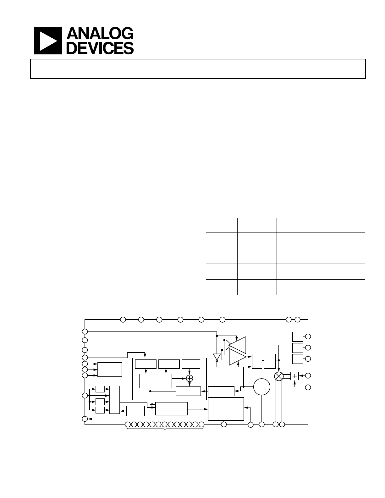
GENERAL DESCRIPTION
The ADRF6603 is a high dynamic range active mixer with
integrated phase-locked loop (PLL) and voltage controlled
oscillator (VCO). The PLL/synthesizer uses a fractional-N
PLL to generate a f
can be divided or multiplied and then applied to the PLL phase
frequency detector (PFD).
LODRV_EN
Rev. A
Information furnished by Analog Devices is believed to be accurate and reliable. However, no
responsibility is assumed by Analog Devices for its use, nor for any infringements of patents or other
rights of third parties that may result from its use. Specifications subject to change without notice. No
license is granted by implication or otherwise under any patent or patent rights of Analog Devices.
Trademarks and registered trademarks are the property of their respective owners.
input to the mixer. The reference input
LO
CC1
36
LON
37
38
LOP
PLL_EN
DATA
CLK
REF_IN
MUXOUT
16
12
13
14
LE
6
8
SPI
INTERFACE
×2
MUX
÷2
÷4
FRACTION
TEMP
SENSOR
7 11 15 20 21 23 24 25 28 30 31 35
FUNCTIONAL BLOCK DIAGRAM
CC2VCC_LOVCC_MIXVCC_V2IVCC_LO
PHASE
INTEGER
N COUNTER
21 TO 123
MODULUS
REG
THIRD-ORDER
FRACTIONAL
INTERPOLATOR
–
+
FREQUENCY
DETECTOR
GND
REG
Figure 1.
ADRF6603
The PLL can support input reference frequencies from 12 MHz
to 160 MHz. The PFD output controls a charge pump whose
output drives an off-chip loop filter.
The loop filter output is then applied to an integrated VCO. The
VCO output at 2 × f
programmable PLL divider. The programmable PLL divider is
controlled by a sigma-delta (Σ-) modulator (SDM). The modulus
of the SDM can be programmed from 1 to 2047.
The active mixer converts the single-ended 50 RF input to
a 200 Ω differential IF output. The IF output can operate up
to 500 MHz.
The ADRF6603 is fabricated using an advanced silicon-germanium
BiCMOS process. It is available in a 40-lead, RoHS-compliant,
6 mm × 6 mm LFCSP with an exposed paddle. Performance is
specified over the −40°C to +85°C temperature range.
Table 1.
Internal LO
Part No.
Range
ADRF6601 750 MHz 300 MHz 450 MHz
1160 MHz 2500 MHz 1600 MHz
ADRF6602 1550 MHz 1000 MHz 1350 MHz
2150 MHz 3100 MHz 2750 MHz
ADRF6603 2100 MHz 1100 MHz 1450 MHz
2600 MHz 3200 MHz 2850 MHz
ADRF6604 2500 MHz 1200 MHz 1600 MHz
2900 MHz 3600 MHz 3200 MHz
2717101 22
34
BUFFER
BUFFER
PRESCALER
÷2
CHARGE PUMP
250µA,
500µA (DEFAULT),
750µA,
1000µA
54
R
SET
One Technology Way, P.O. Box 9106, Norwood, MA 02062-9106, U.S.A.
Tel: 781.329.4700 www.analog.com
Fax: 781.461.3113 ©2010 Analog Devices, Inc. All rights reserved.
is applied to an LO divider, as well as to a
LO
±3 dB RF
Balun Range
ADRF6603
INTERNAL L O RANGE
2100MHz TO 2600 M Hz
DIV
2:1
BY
MUX
2, 1
VCO
CORE
3
CP VTUNE
IFP
191839
IFN
NC
32 33
3.3V
LDO
2.5V
LDO
VCO
LDO
NC
IN
2
9
40
26
29
±1 dB RFIN
Balun Range
DECL3P3
DECL2P5
DECLVCO
RF
IN
IP3SET
08547-001

ADRF6603
TABLE OF CONTENTS
Features .............................................................................................. 1
Applications ....................................................................................... 1
General Description ......................................................................... 1
Functional Block Diagram .............................................................. 1
Revision History ............................................................................... 2
Specifications ..................................................................................... 3
RF Specifications .......................................................................... 3
Synthesizer/PLL Specifications ................................................... 4
Logic Input and Power Specifications ....................................... 4
Timing Characteristics ................................................................ 5
Absolute Maximum Ratings ............................................................ 6
ESD Caution .................................................................................. 6
Pin Configuration and Function Descriptions ............................. 7
Typical Performance Characteristics ............................................. 9
RF Frequency Sweep .................................................................... 9
IF Frequency Sweep ................................................................... 10
Spurious Performance................................................................ 15
Register Structure ........................................................................... 16
Register 0—Integer Divide Control (Default: 0x0001C0)..... 16
Register 1—Modulus Divide Control (Default: 0x003001) .. 16
Register 2—Fractional Divide Control
(Default: 0x001802) .................................................................... 17
Register 3—Σ-Δ Modulator Dither Control
(Default: 0x10000B) ................................................................... 17
Register 4—PLL Charge Pump, PFD, and Reference Path
Control (Default: 0x0AA7E4) ................................................... 18
Register 5—PLL Enable and LO Path Control
(Default: 0x0000E5) ................................................................... 19
Register 6—VCO Control and VCO Enable
(Default: 0x1E2106) ................................................................... 19
Register 7—Mixer Bias Enable and External VCO Enable
(Default: 0x000007) .................................................................... 19
Theory of Operation ...................................................................... 20
Programming the ADRF6603 ................................................... 20
Initialization Sequence .............................................................. 20
LO Selection Logic ..................................................................... 21
Applications Information .............................................................. 22
Basic Connections for Operation ............................................. 22
AC Test Fixture ............................................................................... 23
Evaluation Board ............................................................................ 24
Evaluation Board Control Software ......................................... 24
Schematic and Artwork ............................................................. 26
Evaluation Board Configuration Options ............................... 28
Outline Dimensions ....................................................................... 29
Ordering Guide .......................................................................... 29
REVISION HISTORY
11/10—Rev. 0 to Rev. A
Changes to Features and General Description ............................. 1
Changes to Table 1 ............................................................................ 1
Changes to Table 2 ............................................................................ 3
Changes to Table 3 and Table 4 ....................................................... 4
Changes to Table 6 ............................................................................ 6
Change to Table 7, Pin 36 Description .......................................... 8
Changes to Typical Performance Characteristics Section ........... 9
Added Spurious Performance Section ......................................... 15
Changes to Programming the ADRF6603 Section .................... 20
Changes to Figure 46 ...................................................................... 22
Added AC Test Fixture Section and Figure 47;
Renumbered Sequentially ............................................................. 23
Changes to Evaluation Board Control Software Section;
Changes to Figure 48 ...................................................................... 24
Changes to Figure 49 ...................................................................... 25
Changes to Figure 50 ...................................................................... 26
1/10—Revision 0: Initial Version
Rev. A | Page 2 of 32

ADRF6603
SPECIFICATIONS
RF SPECIFICATIONS
VS = 5 V; ambient temperature (TA) = 25°C; f
using CDAC (0x1) and IP3SET (3.3 V), unless otherwise noted.
Table 2.
Parameter Test Conditions/Comments Min Typ Max Unit
INTERNAL LO FREQUENCY RANGE 2100 2600 MHz
RF INPUT FREQUENCY RANGE ±3 dB RF input range 1100 3200 MHz
RF INPUT AT 2140 MHz
Input Return Loss Relative to 50 Ω (can be improved with external match) <(−20) dB
Input P1dB 14.9 dBm
Second-Order Intercept (IIP2) −5 dBm each tone (10 MHz spacing between tones) 55.3 dBm
Third-Order Intercept (IIP3) −5 dBm each tone (10 MHz spacing between tones) 29.3 dBm
Single-Side Band Noise Figure IP3SET = 3.3 V 15.6 dB
IP3SET = open 14.4 dB
LO-to-IF Leakage At 1× LO frequency, 50 Ω termination at the RF port −43 dBm
RF INPUT AT 2400 MHz
Input Return Loss Relative to 50 Ω (can be improved with external match) −16 dB
Input P1dB 14.9 dBm
Second-Order Intercept (IIP2) −5 dBm each tone (10 MHz spacing between tones) 55.1 dBm
Third-Order Intercept (IIP3) −5 dBm each tone (10 MHz spacing between tones) 28.6 dBm
Single-Side Band Noise Figure IP3SET = 3.3 V 15.8 dB
IP3SET = open 14.2 dB
LO-to-IF Leakage At 1× LO frequency, 50 Ω termination at the RF port −43 dBm
RF INPUT AT 2650 MHz
Input Return Loss Relative to 50 Ω (can be improved with external match) −11 dB
Input P1dB 14.7 dBm
Second-Order Intercept (IIP2) −5 dBm each tone (10 MHz spacing between tones) 52.1 dBm
Third-Order Intercept (IIP3) −5 dBm each tone (10 MHz spacing between tones) 28.1 dBm
Single-Side Band Noise Figure IP3SET = 3.3 V 15.8 dB
IP3SET = open 14.5 dB
LO-to-IF Leakage At 1× LO frequency, 50 Ω termination at the RF port −44 dBm
IF OUTPUT
Voltage Conversion Gain Differential 200 Ω load 6.7 dB
IF Bandwidth Small signal 3 dB bandwidth 500 MHz
Output Common-Mode Voltage External pull-up balun or inductors required 5 V
Gain Flatness Over frequency range, any 5 MHz/50 MHz 0.2/1.0 dB
Gain Variation Over full temperature range 1.2 dB
Output Swing Differential 200 Ω load 2 V p-p
Differential Output Return Loss Measured through 4:1 balun −15 dB
LO INPUT/OUTPUT (LOP, LON) Externally applied 1× LO input, internal PLL disabled
Frequency Range 250 6000 MHz
Output Level (LO as Output) 1× LO into a 50 Ω load, LO output buffer enabled −7 dBm
Input Level (LO as Input) −6 0 +6 dBm
Input Impedance 50 Ω
= 153.6 MHz; f
REF
= 38.4 MHz; high-side LO injection; fIF = 140 MHz; IIP3 optimized
PFD
Rev. A | Page 3 of 32

ADRF6603
SYNTHESIZER/PLL SPECIFICATIONS
VS = 5 V; ambient temperature (TA) = 25°C; f
= 140 MHz; IIP3 optimized using CDAC (0x1) and IP3SET (3.3 V), unless otherwise noted.
f
IF
Table 3.
Parameter Test Conditions/Comments Min Typ Max Unit
SYNTHESIZER SPECIFICATIONS Synthesizer specifications referenced to 1× LO
Frequency Range Internally generated LO 2100 2600 MHz
Figure of Merit1 P
Reference Spurs f
f
f
PFD
PFD
PFD
>f
PHASE NOISE fLO = 2100 MHz to 2600 MHz, f
1 kHz to 10 kHz offset −88 dBc/Hz
100 kHz offset −99.5 dBc/Hz
500 kHz offset −120 dBc/Hz
1 MHz offset −128 dBc/Hz
5 MHz offset −142 dBc/Hz
10 MHz offset −148 dBc/Hz
20 MHz offset −150 dBc/Hz
Integrated Phase Noise 1 kHz to 40 MHz integration bandwidth 0.42
PFD Frequency 20 40 MHz
REFERENCE CHARACTERISTICS REF_IN, MUXOUT pins
REF_IN Input Frequency 12 160 MHz
REF_IN Input Capacitance 4 pF
MUXOUT Output Level VOL (lock detect output selected) 0.25 V
V
MUXOUT Duty Cycle 50 %
CHARGE PUMP
Pump Current Programmable to 250 μA, 500 μA, 750 μA, 1 mA 500 μA
Output Compliance Range 1 2.8 V
1
The figure of merit (FOM) is computed as phase noise (dBc/Hz) – 10Log10(f
power = 10 dBm (500 V/μs slew rate) with a 40 MHz f
and f
REF
= 153.6 MHz; f
REF
= 0 dBm −222 dBc/Hz/Hz
REF_IN
power = 4 dBm; f
REF
= 38.4 MHz; high-side LO injection;
PFD
= 38.4 MHz
/4 −107 dBc
−82 dBc
−85 dBc
PFD
= 38.4 MHz
PFD
°rms
(lock detect output selected) 2.7 V
OH
) – 20Log10(fLO/f
. The FOM was computed at 50 kHz offset.
PFD
PFD
). The FOM was measured across the full LO range, with f
PFD
= 80 MHz,
REF
LOGIC INPUT AND POWER SPECIFICATIONS
VS = 5 V; ambient temperature (TA) = 25°C; f
using CDAC (0x1) and IP3SET (3.3 V), unless otherwise noted.
Table 4.
Parameter Test Conditions/Comments Min Typ Max Unit
LOGIC INPUTS CLK, DATA, LE
Input High Voltage, V
Input Low Voltage, V
Input Current, I
1.4 3.3 V
INH
0 0.7 V
INL
0.1 μA
INH/IINL
Input Capacitance, CIN 5 pF
POWER SUPPLIES VCC1, VCC2, VCC_LO, VCC_MIX, and VCC_V2I pins
Voltage Range 4.75 5 5.25 V
Supply Current PLL only 97 mA
External LO mode (internal PLL disabled, LO output buffer off, IP3SET pin = 3.3 V) 164 mA
Internal LO mode (internal PLL enabled, IP3SET pin = 3.3 V, LO output buffer on) 274 mA
Internal LO mode (internal PLL enabled, IP3SET pin = 3.3 V, LO output buffer off) 261 mA
Power-down mode 30 mA
= 153.6 MHz; f
REF
= 38.4 MHz; high-side LO injection; fIF = 140 MHz; IIP3 optimized
PFD
Rev. A | Page 4 of 32
ADRF6603
TIMING CHARACTERISTICS
VCC2 = 5 V ± 5%.
Table 5.
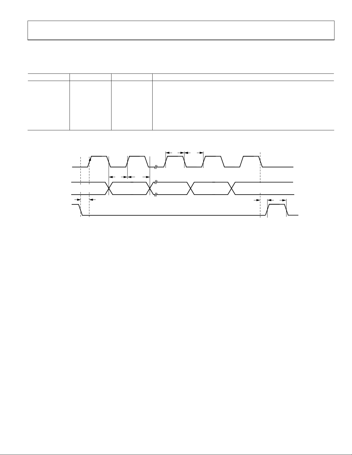
Parameter Limit Unit Description
t1 20 ns min LE setup time
t2 10 ns min DATA-to-CLK setup time
t3 10 ns min DATA-to-CLK hold time
t4 25 ns min CLK high duration
t5 25 ns min CLK low duration
t6 10 ns min CLK-to-LE setup time
t7 20 ns min LE pulse width
Timing Diagram
CLK
t
4
t
5
DATA
DB23 (MSB) DB22
t
1
LE
t
2
t
3
DB2 DB1
(CONTROL BIT C2)(CONTROL BIT C3)
DB0 (LSB)
(CONTROLBIT C1)
t
6
t
7
08547-002
Figure 2. Timing Diagram
Rev. A | Page 5 of 32
ADRF6603
ABSOLUTE MAXIMUM RATINGS
Table 6.
Parameter Rating
Supply Voltage, VCC1, VCC2, VCC_LO,
VCC_MIX, VCC_V2I
Digital I/O, CLK, DATA, LE, LODRV_EN,
PLL_EN
VTUNE 0 V to 3.3 V
IFP, IFN −0.3 V to VCC_V2I + 0.3 V
RFIN 16 dBm
LOP, LON, REF_IN 13 dBm
θJA (Exposed Paddle Soldered Down) 35°C/W
Maximum Junction Temperature 150°C
Operating Temperature Range −40°C to +85°C
Storage Temperature Range −65°C to +150°C
−0.5 V to +5.5 V
−0.3 V to +3.6 V
Stresses above those listed under Absolute Maximum Ratings
may cause permanent damage to the device. This is a stress
rating only; functional operation of the device at these or any
other conditions above those indicated in the operational
section of this specification is not implied. Exposure to absolute
maximum rating conditions for extended periods may affect
device reliability.
ESD CAUTION
Rev. A | Page 6 of 32
ADRF6603
PIN CONFIGURATION AND FUNCTION DESCRIPTIONS
ODRV_EN
NC
VCC_LO
GND
L
LON
DECLVCO
LOP
VTUNE
37
38
39
40
NC
GND
32
31
33
34
35
36
1VCC1
2DECL3P3
3CP
GND
4
R
5
SET
REF_IN
MUXOUT
DECL2P5
NOTES
1. NC = NO CONNECT.
2. THE EXPOSED PADDLE SHOULD BE SOLDERED TO A
LOW IMPEDANCE GROUND PLANE.
GND
VCC2
6
7
8
9
10
PIN 1
INDICATOR
ADRF6603
TOP VIEW
(Not to Scale)
4
11
13
12
1
15
16
LE
CLK
GND
GND
DATA
PLL_EN
30 GND
29 IP3SET
28 GND
27 VCC_V2I
RF
26
IN
25
GND
24 GND
23 GND
22 VCC_MIX
21
GND
20
19
18
17
IFP
IFN
GND
VCC_LO
08547-003
Figure 3. Pin Configuration
Table 7. Pin Function Descriptions
Pin No. Mnemonic Description
1 VCC1
Power Supply for the 3.3 V LDO. Power supply voltage range is 4.75 V to 5.25 V. Each power supply pin
should be decoupled with a 100 pF capacitor and a 0.1 μF capacitor located close to the pin.
2 DECL3P3 Decoupling Node for 3.3 V LDO. Connect a 0.1 μF capacitor between this pin and ground.
3 CP Charge Pump Output Pin. Connect to VTUNE through the loop filter.
4, 7, 11, 15, 20,
GND Ground. Connect these pins to a low impedance ground plane.
21, 23, 24, 25,
28, 30, 31, 35
5 R
SET
Charge Pump Current. The nominal charge pump current can be set to 250 μA, 500 μA, 750 μA, or 1 mA using
Bit DB11 and Bit DB10 in Register 4 and by setting Bit DB18 in Register 4 to 0 (internal reference current). In
this mode, no external R
is required. If Bit DB18 is set to 1, the four nominal charge pump currents (I
SET
can be externally adjusted according to the following equation:
=
R
SET
6 REF_IN
Reference Input. Nominal input level is 1 V p-p. Input range is 12 MHz to 160 MHz. This pin is internally dc-
⎛
⎜
⎜
⎝
I
NOMINAL
⎞
CP
⎟
⎟
⎠
37.8
−
×
I
4.217
biased and should be ac-coupled.
8 MUXOUT
Multiplexer Output. This output can be programmed to provide the reference output signal or the lock detect
signal. The output is selected by programming the appropriate register.
9 DECL2P5 Decoupling Node for 2.5 V LDO. Connect a 0.1 μF capacitor between this pin and ground.
10 VCC2
Power Supply for the 2.5 V LDO. Power supply voltage range is 4.75 V to 5.25 V. Each power supply pin
should be decoupled with a 100 pF capacitor and a 0.1 μF capacitor located close to the pin.
12 DATA Serial Data Input. The serial data input is loaded MSB first; the three LSBs are the control bits.
13 CLK
Serial Clock Input. The serial clock input is used to clock in the serial data to the registers. The data is latched
into the 24-bit shift register on the CLK rising edge. Maximum clock frequency is 20 MHz.
14 LE
Load Enable. When the LE input pin goes high, the data stored in the shift registers is loaded into one of the
eight registers. The relevant latch is selected by the three control bits of the 24-bit word.
16 PLL_EN
PLL Enable. Switch between internal PLL and external LO input. When this pin is logic high, the mixer LO is
automatically switched to the internal PLL and the internal PLL is powered up. When this pin is logic low, the
internal PLL is powered down and the external LO input is routed to the mixer LO inputs. The SPI can also be
used to switch modes.
Rev. A | Page 7 of 32
NOMINAL
)

ADRF6603
Pin No. Mnemonic Description
17, 34 VCC_LO
18, 19 IFP, IFN Mixer IF Outputs. These outputs should be pulled to VCC with RF chokes.
22 VCC_MIX
26 RFIN RF Input (Single-Ended, 50 Ω).
27 VCC_V2I
29 IP3SET Connect a resistor from this pin to a 5 V supply to adjust IIP3. Normally leave open.
32, 33 NC No Connection.
36 LODRV_EN
37, 38 LON, LOP
39 VTUNE
40 DECLVCO Decoupling Node for VCO LDO. Connect a 100 pF capacitor and a 10 μF capacitor between this pin and ground.
EPAD Exposed Paddle. The exposed paddle should be soldered to a low impedance ground plane.
Power Supply. Power supply voltage range is 4.75 V to 5.25 V. Each power supply pin should be decoupled
with a 100 pF capacitor and a 0.1 μF capacitor located close to the pin.
Power Supply. Power supply voltage range is 4.75 V to 5.25 V. Each power supply pin should be decoupled
with a 100 pF capacitor and a 0.1 μF capacitor located close to the pin.
Power Supply. Power supply voltage range is 4.75 V to 5.25 V. Each power supply pin should be decoupled
with a 100 pF capacitor and a 0.1 μF capacitor located close to the pin.
LO Driver Enable. Together with Pin 16 (PLL_EN), this digital input pin determines whether the LOP and LON
pins operate as inputs or outputs. LOP and LON become inputs if the PLL_EN pin is low or if the PLL_EN pin
is set high with the PLEN bit (DB6 in Register 5) set to 0. LOP and LON become outputs if either the LODRV_EN
pin or the LDRV bit (DB3 in Register 5) is set to 1 while the PLL_EN pin is set high. External LO drive frequency
must be 1× LO. This pin has an internal 100 kΩ pull down resistor.
Local Oscillator Input/Output. The internally generated 1× LO is available on these pins. When internal LO
generation is disabled, an external 1× LO can be applied to these pins.
VCO Control Voltage Input. This pin is driven by the output of the loop filter. Nominal input voltage range on
this pin is 1.5 V to 2.5 V.
Rev. A | Page 8 of 32
ADRF6603
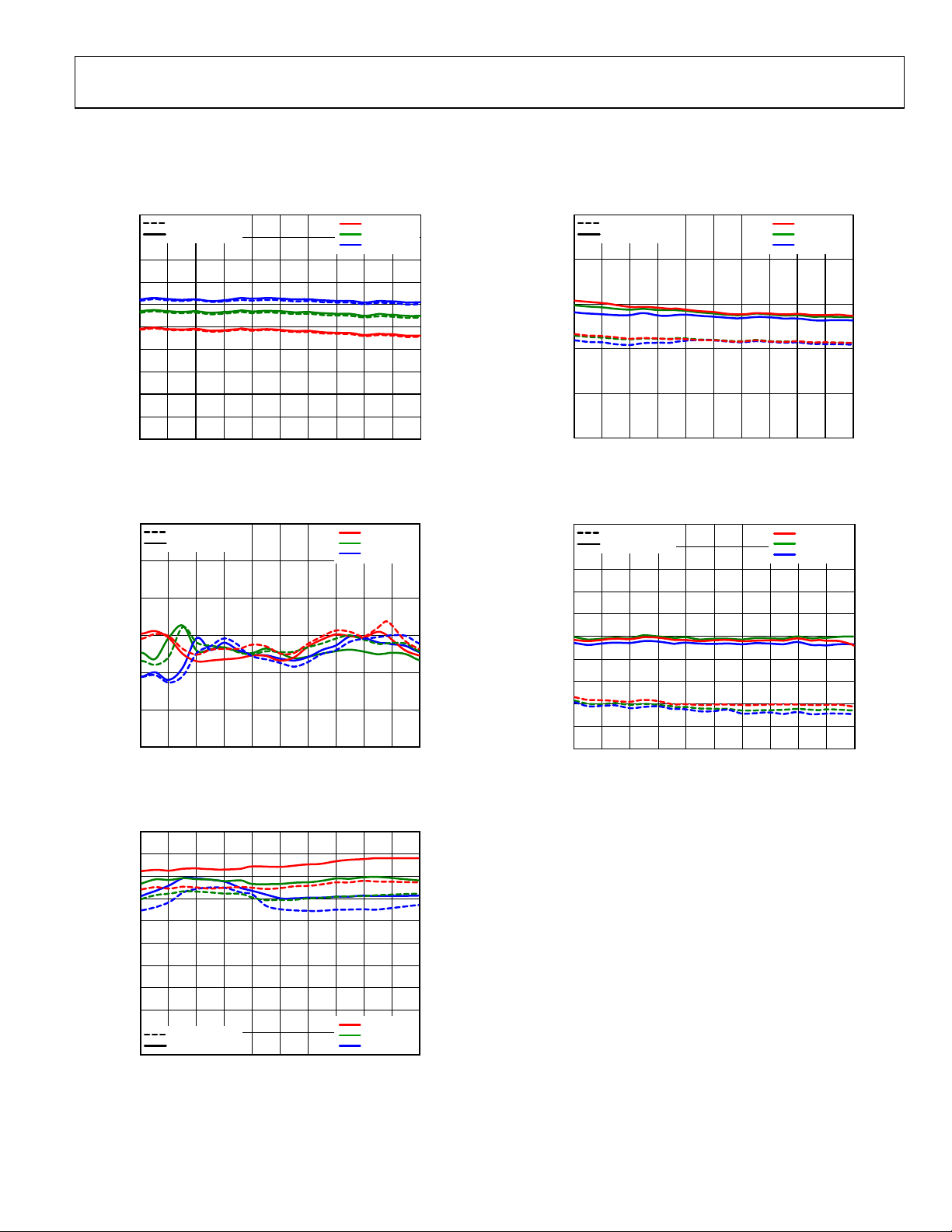
TYPICAL PERFORMANCE CHARACTERISTICS
RF FREQUENCY SWEEP
CDAC = 0x1, internally generated high-side LO, RFIN = −5 dBm, fIF = 140 MHz, unless otherwise noted.
5
IP3SET = OPEN
IP3SET = 3.3V
4
3
2
1
0
GAIN (dB)
–1
–2
–3
–4
–5
1960 2010 2060 2110 2160 2210 2260 2310 2360 2410 2460
RF FREQUENCY (MHz)
TA = +85°C
TA = +25°C
TA = –40°C
Figure 4. Gain vs. RF Frequency
08547-104
40
IP3SET = OPEN
IP3SET = 3.3V
35
30
25
INPUT IP3 (dBm)
20
15
1960 2010 2060 2110 2160 2210 2260 2310 2360 2410 2460
RF FREQUENCY ( MHz)
TA = +85°C
TA = +25°C
TA = –40°C
Figure 7. Input IP3 vs. RF Frequency
08547-107
90
IP3SET = OPEN
IP3SET = 3.3V
80
70
60
INPUT IP2 (dBm)
50
40
30
1960 2010 2060 2110 2160 2210 2260 2310 2360 2410 2460
RF FREQUENCY ( MHz)
TA = +85°C
TA = +25°C
TA = –40°C
Figure 5. Input IP2 vs. RF Frequency
20
18
16
14
12
10
8
NOISE FIGURE (dB)
6
4
2
IP3SET = OPEN
IP3SET = 3.3V
0
1960 2010 2060 2110 2160 2210 2260 2310 2360 2410 2460
RF FREQUENCY ( MHz)
TA = +85°C
TA = +25°C
TA = –40°C
Figure 6. Noise Figure vs. RF Frequency
20
IP3SET = OPEN
IP3SET = 3.3V
19
18
17
16
15
14
INPUT P1dB (dBm)
13
12
11
10
1960 2010 2060 2110 2160 2210 2260 2310 2360 2410 2460
08547-105
RF FREQUENCY (MHz)
TA = +85°C
TA = +25°C
TA = –40°C
08547-108
Figure 8. Input P1dB vs. RF Frequency
08547-106
Rev. A | Page 9 of 32
ADRF6603
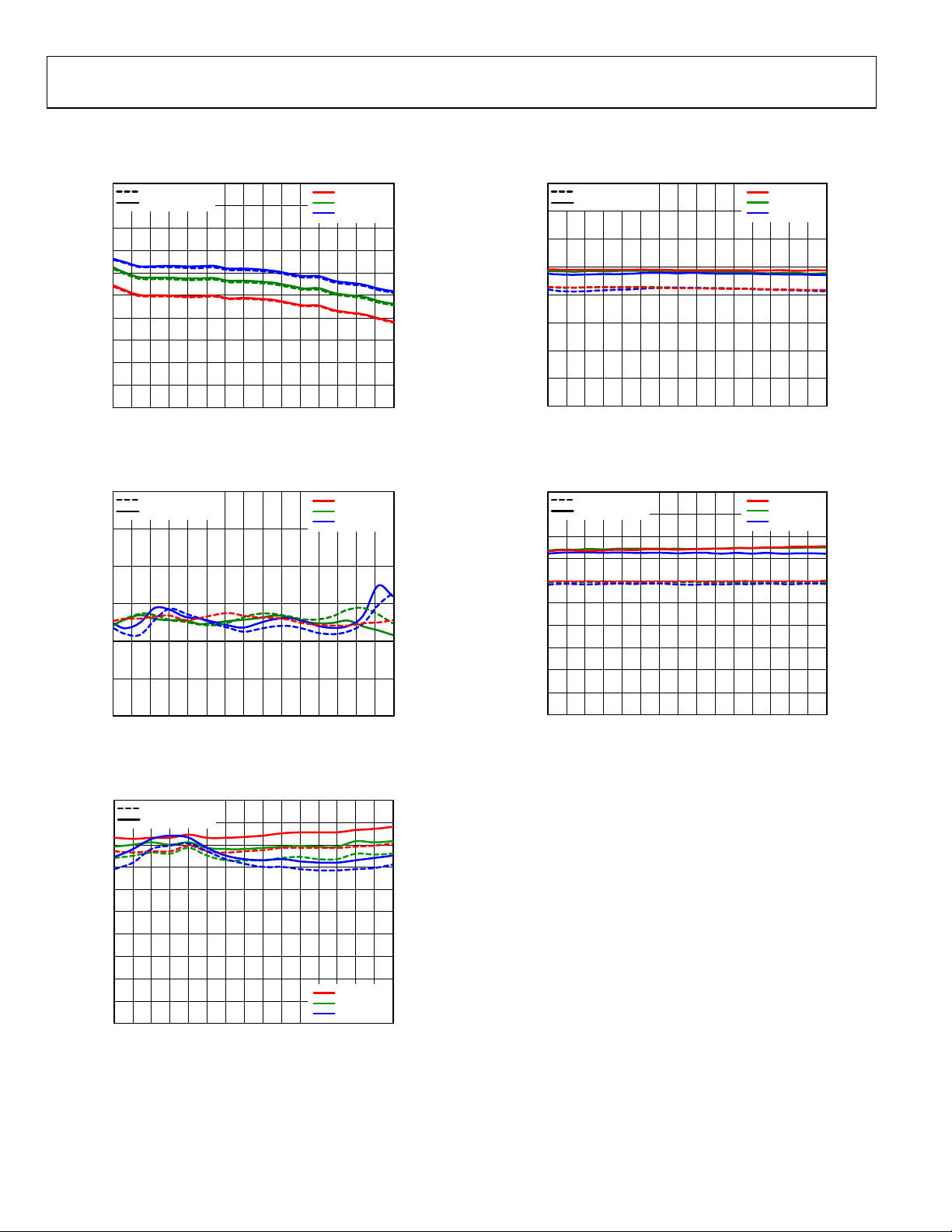
IF FREQUENCY SWEEP
CDAC = 0x1, internally generated swept low-side LO, fRF = 1960 MHz, RFIN = −5 dBm, unless otherwise noted.
5
IP3SET = OPEN
IP3SET = 3.3V
4
3
2
1
0
GAIN (dB)
–1
–2
–3
–4
–5
25 50 75 100 125 150 175 200 225 250 275 300 325 350 375 400
IF FR E QUENCY (MHz)
Figure 9. Gain vs. IF Frequency
TA = +85°C
TA = +25°C
TA = –40°C
08547-109
45
IP3SET = OPEN
IP3SET = 3.3V
40
35
30
25
20
INPUT IP3 (dBm)
15
10
5
25 4003753503253002752502252001751501257550 100
IF FREQ UE NCY ( MHz)
Figure 12. Input IP3 vs. IF Frequency, RF
TA = +85°C
TA = +25°C
TA = –40°C
= −5 dBm
IN
08547-112
90
IP3SET = OPEN
IP3SET = 3.3V
80
70
60
INPUT IP2 (dBm)
50
40
30
25 50 75 100 125 150 175 200 225 250 275 300 325 350 375 400
Figure 10. Input IP2 vs. IF Frequency, RF
20
IP3SET = OPEN
IP3SET = 3.3V
18
16
14
12
10
8
NOISE FI GURE (dB)
6
4
2
0
25 4003753503253002752502252001751501257550 100
IF FR E QUENCY (MHz)
IF FREQ UE NCY ( MHz)
= −5 dBm
IN
Figure 11. Noise Figure vs. IF Frequency
TA = +85°C
TA = +25°C
TA = –40°C
TA = +85°C
TA = +25°C
TA = –40°C
20
IP3SET = OPEN
IP3SET = 3.3V
18
16
14
12
10
8
INPUT P1dB (dBm)
6
4
2
0
25 4003753503253002752502252001751501257550 100
08547-110
IF FREQ UE NCY ( MHz)
TA = +85°C
TA = +25°C
TA = –40°C
08547-113
Figure 13. Input P1dB vs. IF Frequency
08547-111
Rev. A | Page 10 of 32
 Loading...