30 MHz Dual Programmable Filters
V
Data Sheet
FEATURES
Matched pair of programmable filters and VGAs
Continuous gain control range: −5 dB to +45 dB
6-pole filter
1 MHz to 30 MHz in 1 MHz steps, 0.5 dB corner frequency
SPI programmable
6 dB front-end gain step
IMD3: >55 dBc for 1.5 V p-p composite output
HD2, HD3: >60 dBc for 1.5 V p-p output
Differential input and output
Adjustable output common-mode voltage
Optional dc output offset correction
Power-down feature
Single 5 V supply operation
APPLICATIONS
Baseband I/Q receivers
Diversity receivers
ADC drivers
and Variable Gain Amplifiers
ADRF6510
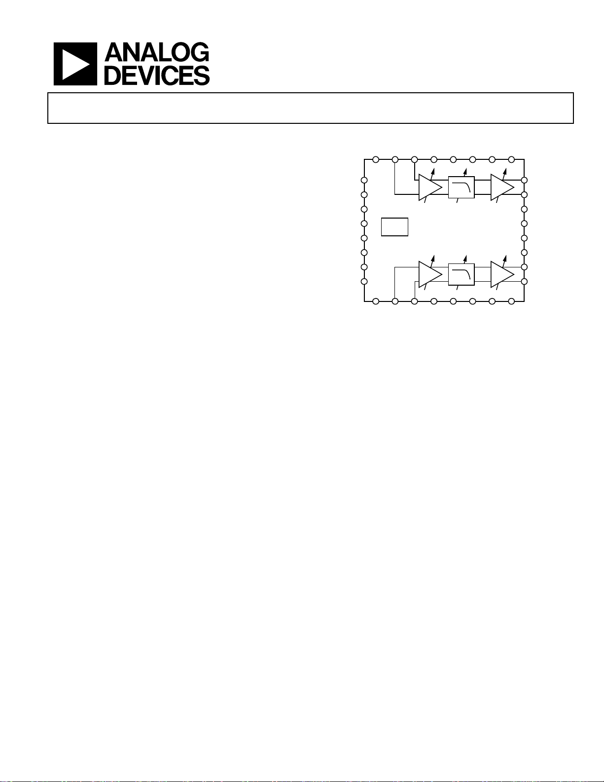
FUNCTIONAL BLOCK DIAGRAM
INP1 INM1
ENBL
VPSD
COMD
LE
CLK
DATA
SDO
COM
VPS
SPI
COM I NP2 INM2 VPS COM OFDS OFS2 V PS
PS
COM GNSW OFS1VPS
ADRF6510
Figure 1.
OPP1
OPM1
COM
GAIN
VOCM
COM
OPM2
OPP2
09002-001
GENERAL DESCRIPTION
The ADRF6510 is a matched pair of fully differential low noise
and low distortion programmable filters and variable gain amplifiers (VGAs). Each channel is capable of rejecting large out-ofband interferers while reliably boosting the wanted signal, thus
reducing the bandwidth and resolution requirements on the
analog-to-digital converters (ADCs). The excellent matching
between channels and their high spurious-free dynamic range
over all gain and bandwidth settings makes the ADRF6510
ideal for quadrature-based (IQ) communication systems with
dense constellations, multiple carriers, and nearby interferers.
The filters provide a six-pole Butterworth response with 0.5 dB
corner frequencies programmable through the SPI port from
1 MHz to 30 MHz in 1 MHz steps. The preamplifier that precedes
the filters offers a pin-programmable option of either 6 dB or
12 dB of gain. The preamplifier sets a differential input impedance of 400 and has a common-mode voltage that defaults
to 2.1 V but can be driven from 1.5 V to 2.5 V.
The variable gain amplifiers that follow the filters provide 50 dB
of continuous gain control with a slope of 30 mV/dB. The output
buffers provide a differential output impedance of 20 Ω that is
capable of driving 1.5 V p-p into 1 kΩ loads. The output commonmode voltage defaults to VPS/2, but it can be programmed via the
VOCM pin. The built-in dc offset correction loop can be disabled
if dc-coupled operation is desired. The high-pass corner frequency
is defined by external capacitors on the OFS1 and OFS2 pins.
The ADRF6510 operates from a 4.75 V to 5.25 V supply and
consumes a maximum supply current of 258 mA when programmed to the highest bandwidth setting. When disabled, it
consumes 2 mA. The ADRF6510 is fabricated in an advanced
silicon-germanium BiCMOS process and is available in a
32-lead, exposed paddle LFCSP. Performance is specified over
the −40°C to +85°C temperature range.
Rev. A
Information furnished by Analog Devices is believed to be accurate and reliable. However, no
responsibility is assumed by Anal og Devices for its use, nor for any infringements of patents or ot her
rights of third parties that may result from its use. Specifications subject to change without notice. No
license is granted by implication or otherwise under any patent or patent rights of Analog Devices.
Trademarks and registered trademarks are the property of their respective owners.
One Technology Way, P.O. Box 9106, Norwood, MA 02062-9106, U.S.A.
Tel: 781.329.4700 www.analog.com
Fax: 781.461.3113 ©2010-2011 Analog Devices, Inc. All rights reserved.

ADRF6510 Data Sheet
TABLE OF CONTENTS
Features.............................................................................................. 1
Applications....................................................................................... 1
Functional Block Diagram ..............................................................1
General Description......................................................................... 1
Revision History ...............................................................................2
Specifications..................................................................................... 3
Timing Diagrams.......................................................................... 5
Absolute Maximum Ratings............................................................ 6
ESD Caution.................................................................................. 6
Pin Configuration and Function Descriptions............................. 7
Typical Performance Characteristics............................................. 8
Theory of Operation ......................................................................15
Input Buffers ...............................................................................15
Programmable Filters.................................................................15
Variable Gain Amplifiers (VGAs)............................................ 16
Output Buffers/ADC Drivers ................................................... 16
DC Offset Compensation Loop................................................ 16
Programming the Filters............................................................17
Noise Characteristics .................................................................17
Distortion Characteristics......................................................... 18
Maximizing the Dynamic Range.............................................. 18
Key Parameters for Quadrature-Based Receivers.................. 19
Applications Information.............................................................. 20
Basic Connections...................................................................... 20
Error Vector Magnitude (EVM) Performance........................... 20
EVM............................................................................................. 21
Effect of Filter Bandwidth on EVM......................................... 21
Effect of Output Voltage Levels on EVM ................................ 21
Effect of C
Anti-Aliasing Filter.................................................................... 22
Evaluation Board............................................................................ 24
Evaluation Board Control Software......................................... 24
Schematics and Artwork ...........................................................24
Evaluation Board Configuration Options............................... 27
Outline Dimensions....................................................................... 29
Ordering Guide .......................................................................... 29
on EVM ............................................................... 22
OFS
REVISION HISTORY
10/11—Rev. 0 to Rev. A
Changes to Figure 2 and Figure 3................................................... 5
Changes to Table 3............................................................................ 7
Changes to Figure 48, Changes to Error Vector Magnitude
(EVM) Performance Section......................................................... 20
Deleted Low IF Image Rejection Section, and Example
Baseband Interface Section, Figure 50, and Figure 51;
Renumbered Subsequent Figures................................................. 20
Changes to Figure 49...................................................................... 21
Added EVM Section, Effect of Filter Bandwidth on EVM
Section, Effect of Output Voltage Levels on EVM Section, and
Effect of C
Added Anti-Aliasing Filter Section.............................................. 22
Changes to Figure 54...................................................................... 22
Changes to Figure 58...................................................................... 24
Changes to Figure 61...................................................................... 25
Changes to Figure 62 and Figure 63............................................. 26
Changes to Table 5.......................................................................... 27
4/10—Revision 0: Initial Version
on EVM Section...................................................... 21
OFS
Rev. A | Page 2 of 32

Data Sheet ADRF6510
SPECIFICATIONS
VPS = 5 V, TA = 25°C, Z
Table 1.
Parameter Test Conditions/Comments Min Typ Max Unit
FREQUENCY RESPONSE
Low-Pass Corner Frequency, fC Six-pole Butterworth filter, 0.5 dB bandwidth 1 30 MHz
Step Size 1 MHz
Corner Frequency Absolute
Accuracy
Corner Frequency Matching
Pass-Band Ripple 0.5 dB p-p
Gain Matching
Group Delay Variation From midband to peak
Corner Frequency = 1 MHz 135 ns
Corner Frequency = 30 MHz 11 ns
Group Delay Matching Channel A and Channel B at same gain
Corner Frequency = 1 MHz 5 ns
Corner Frequency = 30 MHz 0.2 ns
Stop-Band Rejection
Relative to Pass Band 2 × fC 30 dB
5 × fC 75 dB
INPUT STAGE INP1, INM1, INP2, INM2
Maximum Input Swing At minimum gain, V
Differential Input Impedance 400 Ω
Input Common-Mode Range 1 V p-p input voltage 1.5 VPS/2 V
Input pins left floating VPS/2 V
GAIN CONTROL GAIN, GNSW
Voltage Gain Range GNSW = 0 V, V
GNSW = 5 V 1 51 dB
Gain Slope 30 mV/dB
Gain Error V
Gain Step GNSW = 0 V to 5 V 6 dB
OUTPUT STAGE OPP1, OPM1, OPP2, OPM2, VOCM
Maximum Output Swing At maximum gain, R
HD2 > 60 dBc, HD3 > 60 dBc 1.5 V p-p
Differential Output Impedance 20 Ω
Output DC Offset Inputs shorted, offset loop disabled 35 mV
Output Common-Mode Range 1.5 V p-p output voltage 1.5 3.0 V
VOCM left floating VPS/2 V
NOISE/DISTORTION
1 MHz Corner Frequency
Output Noise Density Gain = 0 dB at fC/2 −129 dBV/√Hz
Gain = 20 dB at fC/2 −127 dBV/√Hz
Gain = 40 dB at fC/2 −111 dBV/√Hz
Second Harmonic, HD2 250 kHz fundamental, 1.5 V p-p output voltage
Gain = 0 dB 46.2 dBc
Gain = 40 dB 43.2 dBc
Third Harmonic, HD3 250 kHz fundamental, 1.5 V p-p output voltage
Gain = 0 dB 52.2 dBc
Gain = 40 dB 51.2 dBc
SOURCE
= 400 Ω, Z
= 1 kΩ, V
LOAD
= 1.5 V p-p, bandwidth setting = 30 MHz, GNSW = 0 V, unless otherwise noted.
OUT
Over operating temperature range ±15 % f
Channel A and Channel B at same gain and
±0.5 % f
bandwidth settings
Channel A and Channel B at same gain and
±0.1 dB
bandwidth settings
= 0 V 1 V p-p
GAIN
from 0 V to 2 V −5 +45 dB
GAIN
from 500 mV to 1.7 V 0.2 dB
GAIN
= 1 kΩ 2 V p-p
LOAD
C
C
Rev. A | Page 3 of 32

ADRF6510 Data Sheet
Parameter Test Conditions/Comments Min Typ Max Unit
IMD3
f1 = 500 kHz, f2 = 550 kHz, 1.5 V p-p composite
output voltage
Gain = 5 dB 61 dBc
Gain = 35 dB 57 dBc
IMD3 with Input CW Blocker
f1 = 500 kHz, f2 = 550 kHz, 1.5 V p-p composite
output, gain = 5 dB; blocker at 5 MHz, 10 dBc
relative to two-tone composite output voltage
30 MHz Corner Frequency
Output Noise Density Midband, gain = 0 dB −130 dBV/√Hz
Midband, gain = 20 dB −130 dBV/√Hz
Midband, gain = 40 dB −123 dBV/√Hz
Second Harmonic, HD2 8 MHz fundamental, 1.5 V p-p output voltage
Gain = 0 dB 63 dBc
Gain = 40 dB 84 dBc
Third Harmonic, HD3 8 MHz fundamental, 1.5 V p-p output voltage
Gain = 0 dB 54 dBc
Gain = 40 dB 87 dBc
IMD3
f1 = 15 MHz, f2 = 16 MHz, 1.5 V p-p composite
output voltage
Gain = 5 dB 59 dBc
Gain = 35 dB 77.5 dBc
IMD3 with Input CW Blocker
f1 = 15 MHz, f2 = 16 MHz, 1.5 V p-p composite
output, gain = 5 dB; blocker at 150 MHz, 10 dBc
relative to two-tone composite output voltage
DIGITAL LOGIC LE, CLK, DATA, SDO, OFDS, GNSW
Input High Voltage, V
Input Low Voltage, V
Input Current, I
INH/IINL
>2 V
INH
<0.8 V
INL
<1 μA
Input Capacitance, CIN 2 pF
SPI TIMING LE, CLK, DATA, SDO
f
1/t
CLK
20 MHz
CLK
tDH DATA hold time 5 ns
tDS DATA setup time 5 ns
tLH LE hold time 5 ns
tLS LE setup time 5 ns
tPW CLK high pulse width 5 ns
tD CLK to SDO delay 5 ns
POWER AND ENABLE VPS, VPSD, COM, COMD, ENBL
Supply Voltage Range 4.75 5.0 5.25 V
Total Supply Current ENBL = 5 V
Maximum bandwidth setting 258 mA
Minimum bandwidth setting 131 mA
Disable Current ENBL = 0 V 2 mA
Disable Threshold 2.5 V
Enable Response Time Delay following ENBL low-to-high transition 20 μs
Disable Response Time Delay following ENBL high-to-low transition 300 ns
40 dBc
55 dBc
Rev. A | Page 4 of 32
Data Sheet ADRF6510
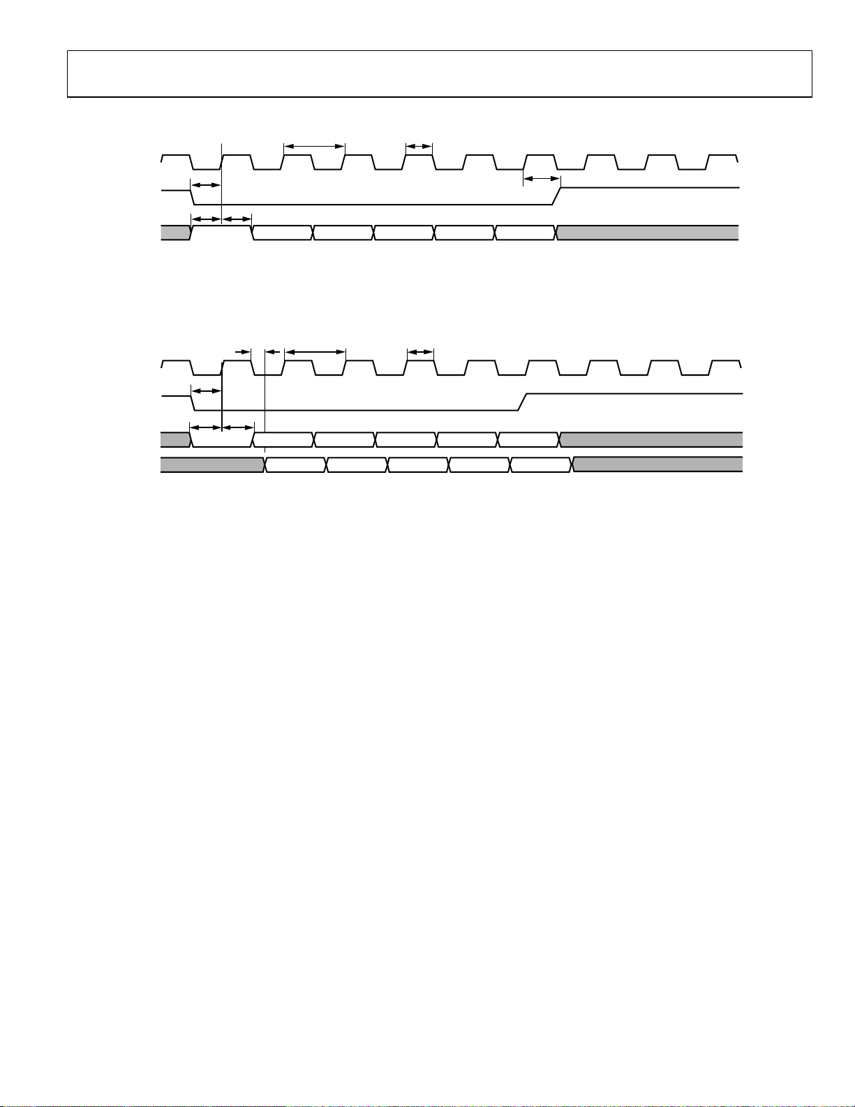
TIMING DIAGRAMS
t
CLK
CLK
LE
DATA
NOTES
1. THE FIRST DATA BIT DETERMINES WHETHER THE PART IS WRITING TO OR READING F ROM THE I NTERNAL CORNER FREQUENC Y
WORD REGISTER. FOR A WRITE O PERATION, THE FIRST BIT SHO ULD BE A LOGIC 1. THE CORNER FREQUENCY WORD BIT I S THEN
REGISTERE D INTO THE DATA PIN ON CONSECUTIVE RISING EDGES O F THE CLO CK.
t
LS
tDSt
DH
WRITE BIT
LSB + 1LSB
Figure 2. Write Mode Timing Diagram
t
CLK
DCDCREAD BIT DC DC DC
CLK
LE
DATA
t
t
LS
tDSt
D
DH
t
PW
MSB – 2 MSB – 1 MSB
t
PW
MSB - 2
t
LH
09002-003
SDO
NOTES
1. THE FIRST DAT A BIT DET ERMINES WHETHER T HE PART I S WRIT ING TO OR READING FROM T HE INTE RNAL CORNER FREQUENCY WORD
REGIST ER. FO R A READ OPERAT ION, THE FI RST BIT SHOULD BE A LOGI C 0. THE CO RNER FREQ UENCY WORD BIT IS THEN UPDATED AT
THE SDO PIN ON CONSECUTIVE FALLING EDGES OF THE CLOCK.
LSB + 1LSB
MSB – 2
MSB – 1 MSB
09002-004
Figure 3. Read Mode Timing Diagram
Rev. A | Page 5 of 32
ADRF6510 Data Sheet
ABSOLUTE MAXIMUM RATINGS
Table 2.
Parameter Rating
Supply Voltages, VPS, VPSD 5.25 V
ENBL, GNSW, OFDS, LE, CLK, DATA, SDO VPS + 0.6 V
INP1, INM1, INP2, INM2
OPP1, OPM1, OPP2, OPM2 VPS + 0.6 V
OFS1, OFS2 VPS + 0.6 V
GAIN VPS + 0.6 V
Internal Power Dissipation 1.4 W
θJA (Exposed Pad Soldered to Board) 37.4°C/W
Maximum Junction Temperature 150°C
Operating Temperature Range −40°C to +85°C
Storage Temperature Range −65°C to +150°C
Lead Temperature (Soldering 60 sec) 300°C
VPS + 0.6 V,
GND − 0.6 V
Stresses above those listed under Absolute Maximum Ratings
may cause permanent damage to the device. This is a stress
rating only; functional operation of the device at these or any
other conditions above those indicated in the operational
section of this specification is not implied. Exposure to absolute
maximum rating conditions for extended periods may affect
device reliability.
ESD CAUTION
Rev. A | Page 6 of 32

Data Sheet ADRF6510
W
PIN CONFIGURATION AND FUNCTION DESCRIPTIONS
L
M1
COM
GNS
OFS1
ENB
INP1
IN
31
30
32
VPS
VPS
26
25
28
27
29
1VPSD
PIN 1
2COMD
INDICATOR
3LE
4CLK
ADRF6510
5DATA
TOP VIEW
6SDO
(Not to Scal e)
7COM
8VPS
1
9
1
10
12
13
VPS
INP2
COM
COM
INM2
NOTES
1. CONNECT THE EXPOSED PADDLE TO
A LOW IMPEDANCE GROUND PAD.
24 OPP1
23 O PM1
22 CO M
21 G AIN
20 V OCM
19 CO M
18 O PM2
17 O PP2
14
15
16
VPS
OFS2
OFDS
09002-002
Figure 4. Pin Configuration
Table 3. Pin Function Descriptions
Pin No. Mnemonic Description
1 VPSD Digital Positive Supply Voltage: 4.75 V to 5.25 V.
2 COMD Digital Common. Connect to external circuit common using the lowest possible impedance.
3 LE Latch Enable. SPI programming pin. CMOS levels: V
4 CLK SPI Port Clock. CMOS levels: V
5 DATA SPI Data Input. CMOS levels: V
6 SDO SPI Data Output. CMOS levels: V
< 0.8 V, V
LOW
< 0.8 V, V
LOW
LOW
< 0.8 V, V
HIGH
HIGH
> 2 V.
> 2 V.
HIGH
LOW
> 2 V.
< 0.8 V, V
HIGH
> 2 V.
7, 9, 13, 19, 22, 28 COM Analog Common. Connect to external circuit common.
8, 12, 16, 25, 29 VPS Analog Positive Supply Voltage: 4.75 V to 5.25 V.
10, 11, 30, 31
INP2, INM2,
Differential Inputs. 400 Ω input impedance. Common-mode range is 1.5 V to 2.5 V; default is 2.1 V.
INM1, INP1
14 OFDS Offset Correction Loop Disable. Pull high to disable the offset correction loop.
15, 26 OFS2, OFS1 Offset Correction Loop Compensation Capacitors. Connect capacitors to circuit common.
17, 18, 23, 24
OPP2, OPM2,
Differential Outputs. 20 Ω output impedance. Common-mode range is 1.5 V to 3 V; default is VPS/2.
OPM1, OPP1
20 VOCM Output Common-Mode Setpoint. Defaults to VPS/2 if left open.
21 GAIN Analog Gain Control. 0 V to 2 V, 30 mV/dB gain scaling.
27 GNSW Front-End Gain Switch, 6 dB or 12 dB. Pull low for 6 dB; pull high for 12 dB.
32 ENBL Chip Enable. Pull high to enable.
EP Exposed Paddle. Connect the exposed paddle to a low impedance ground pad.
Rev. A | Page 7 of 32
ADRF6510 Data Sheet
TYPICAL PERFORMANCE CHARACTERISTICS
VPS = 5 V, TA = 25°C, Z
50
BANDWIDTH = 30MHz
45
40
35
30
25
20
–40°C
VPS = 4.75V, 5V, 5.25V
15
GAIN (dB)
10
5
0
–5
–10
0 200 400 600 800 1000 1200 1400 1600 1800 22002000
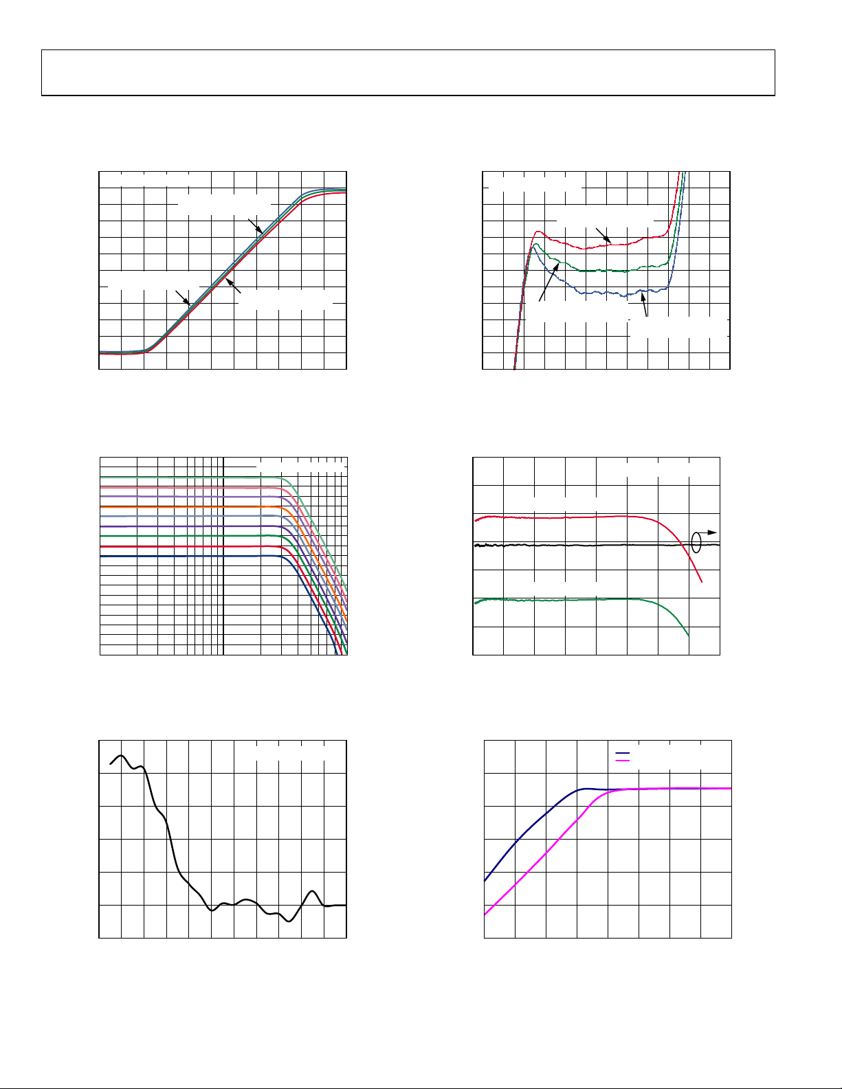
Figure 5. In-Band Gain vs. V
(Bandwidth Setting = 30 MHz)
= 400 Ω, Z
SOURCE
+25°C
VPS = 4.75V, 5V, 5.25V
+85°C
VPS = 4.75V, 5V, 5.25V
V
(mV)
GAIN
over Supply and Temperature
GAIN
= 1 kΩ, V
LOAD
= 1.5 V p-p, GNSW = 0 V, unless otherwise noted.
OUT
3.0
BANDWIDTH = 30MHz
2.5
2.0
1.5
1.0
0.5
0
–0.5
–1.0
GAIN ERROR (dB)
–1.5
–2.0
–2.5
–3.0
0 200 400 600 800 1000 1200 1400 1600 1800 2000 2200 2400
09002-005
+85°C
VPS = 4.25V, 5V, 5.25V
+25°C
VPS = 4.25V, 5V, 5.25V
Figure 8. Gain Conformance vs. V
(Bandwidth Setting = 30 MHz)
–40°C
VPS = 4.25V, 5V, 5.25V
V
(mV)
GAIN
over Supply and Temperature
GAIN
09002-008
50
45
40
35
30
25
20
15
10
5
0
–5
GAIN (dB)
–10
–15
–20
–25
–30
–35
–40
–45
–50
1 10 100
Figure 6. Gain vs. Frequency by V
0.25
0.20
0.15
0.10
FREQUENCY (MHz)
GAIN
BANDWIDTH = 30MHz
(Bandwidth Setting = 30 MHz)
BANDWIDTH = 30MHz
5
3
1
–1
–3
GAIN ERROR (dB)
–5
–7
–9
09002-006
PREAMP GAIN = 12dB
PREAMP GAIN = 6dB
0 5 10 15 4035302520
FREQUENCY (MHz )
BANDWIDTH = 30MHz
9
8
7
6
5
GAIN STEP (dB)
4
3
2
09002-009
Figure 9. 6 dB Gain Step and Gain Error vs. Frequency
(Bandwidth Setting = 30 MHz, V
15
10
5
0
= 0 V)
GAIN
PREAMP GAIN = 6dB
PREAMP GAIN = 12dB
0.05
GAIN MISMATCH (dB)
0
–0.05
02
0.20.40.60.81.01.21.41.61.82.0 .2
Figure 7. Gain Matching vs. V
V
(V)
GAIN
(Bandwidth Setting = 30 MHz)
GAIN
09002-007
OP1dB (dBV rms)
–5
–10
–15
0 5 10 15 20 25 30 35 40
Figure 10. Output P1dB vs. GAIN at 15 MHz (Bandwidth Setting = 30 MHz)
Rev. A | Page 8 of 32
GAIN (dB)
09002-010
Data Sheet ADRF6510
40
35
30
25
20
15
GAIN (dB)
10
5
0
–5
–10
1M 100M10M
FREQUENCY (Hz)
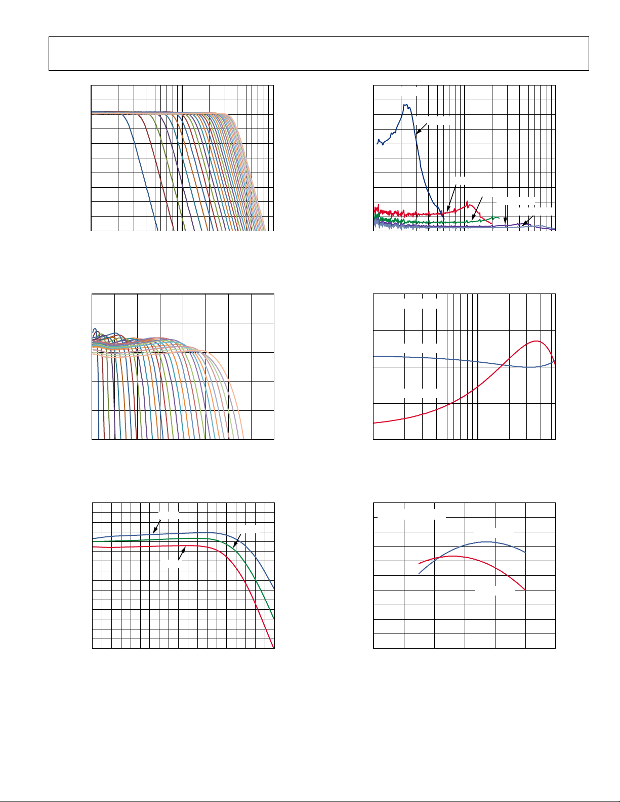
Figure 11. Frequency Response vs. Bandwidth Setting (Gain = 30 dB),
Log Scale
09002-011
1000
GAIN = 20dB
900
800
700
600
500
400
GROUP DELAY (ns)
300
200
100
0
0.5 5 50
BW = 1MHz
BW = 5MHz
BW = 10MHz
BW = 20MHz
FREQUENCY (MHz )
Figure 14. Group Delay vs. Frequency (Gain = 20 dB)
BW = 30MHz
09002-014
32
31
30
GAIN (dB)
29
28
27
140
6 111621263136
FREQUENCY (MHz)
09002-012
Figure 12. Frequency Response vs. Bandwidth Setting (Gain = 30 dB),
1.0
BANDWIDTH = 30MHz
0.5
0
–0.5
GROUP DELAY MATCHING (ns)
–1.0
0.5 5 30
Figure 15. Group Delay Mismatch vs. Frequency
Linear Scale
30
29
28
27
26
25
24
23
22
GAIN (dB)
21
20
19
18
17
16
15
4 6 8 101214161820222426283032343638
240
–40°C
+85°C
FREQUENCY (MHz )
+25°C
09002-013
Figure 13. Frequency Response over Temperature
5
BANDWIDTH = 1MHz
4
3
2
1
0
–1
–2
–3
IQ GROUP DE LAY MATCHING (ns)
–4
–5
0.2 0. 4 0.6 0.8 1.0 1. 2 1. 4
Figure 16. IQ Group Delay Mismatch vs. Frequency
(Gain = 26 dB, Bandwidth Setting = 30 MHz)
GAIN = 20dB
GAIN = 40dB
FREQUENCY (MHz )
(Bandwidth Setting = 30 MHz)
GAIN = 20dB
GAIN = 0dB
FREQUENCY (MHz )
(Bandwidth Setting = 1 MHz)
09002-015
09002-016
Rev. A | Page 9 of 32
ADRF6510 Data Sheet
0 0.51.01.52.02.53.0
0.75
0.50
0.25
BANDWIDTH = 30MHz
0
–0.25
IQ AMPLITUDE MISMAT CH (dB)
–0.50
–0.75
03
5 10152025
FREQUENCY (MHz )
FREQUENCY (MHz )
BANDWIDTH = 1MHz
0
09002-017
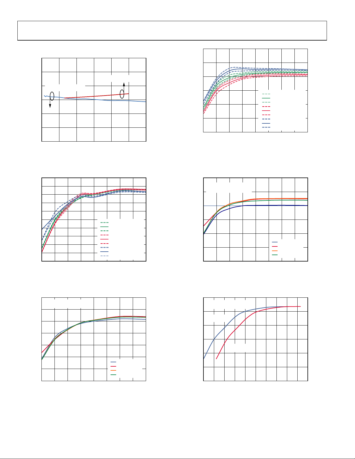
Figure 17. IQ Amplitude Mismatch vs. Frequency
100
90
80
70
60
HD3 @ 24MHz (dBc)
50
40
04
5 101520253035
GAIN (dB)
+25°C, VPS = 4.75V
+25°C, VPS = 5V
+25°C, VPS = 5.25V
+85°C, VPS = 4.75V
+85°C, VPS = 5V
+85°C, VPS = 5.25V
–40°C, VPS = 4.75V
–40°C, VPS = 5V
–40°C, VPS = 5.25V
0
09002-020
Figure 20. HD3 vs. Gain over Supply and Temperature
(Bandwidth Setting = 30 MHz)
90
85
80
75
70
65
60
HD2 @ 16MHz (dBc)
55
50
45
40
040
5 101520253035
GAIN (dB)
+25°C, VPS = 4.75V
+25°C, VPS = 5V
+25°C, VPS = 5.25V
+85°C, VPS = 4.75V
+85°C, VPS = 5V
+85°C, VPS = 5.25V
–40°C, VPS = 4.75V
–40°C, VPS = 5V
–40°C, VPS = 5.25V
09002-018
Figure 18. HD2 vs. Gain over Supply and Temperature
100
1.5V p-p OUTPUT @ 8MHz
BANDWIDTH = 30MHz
90
80
70
60
HD3 @ 24MHz (dBc)
50
40
04
5 101520253035
Figure 21. HD3 vs. Gain over Output Common-Mode Voltage
(Bandwidth Setting = 30 MHz)
100
1.5V p-p OUTPUT @ 8MHz
BANDWIDTH = 30MHz
90
80
70
60
HD2 @ 16MHz (dBc)
50
40
30
0 5 10 15 20 25 30 35 40
GAIN (dB)
VOCM = 1.5V
VOCM = 1.75V
VOCM = 2V
VOCM = 2.5V
Figure 19. HD2 vs. Gain over Output Common-Mode Voltage
09002-019
30
BANDWIDTH = 30MHz
f1 = 14MHz, f2 = 15MHz
25
PREAMP
GAIN = 6dB
20
15
OIP3 (dBV)
10
5
0
05 504540353025201510
Figure 22. In-Band OIP3 vs. Gain (Bandwidth Setting = 30 MHz)
(Bandwidth Setting = 30 MHz)
GAIN (dB)
(Bandwidth Setting = 30 MHz)
PREAMP
GAIN = 12dB
GAIN (dB)
VOCM = 1.5V
VOCM = 1.75V
VOCM = 2V
VOCM = 2.5V
0
09002-021
09002-022
Rev. A | Page 10 of 32
 Loading...