

1.8 V, Micropower, Zero-Drift,
FEATURES
Very low supply current: 13 μA typical
Low offset voltage: 15 μV maximum
Offset voltage drift: 20 nV/°C
Single-supply operation: 1.8 V to 5.5 V
High PSRR: 110 dB minimum
High CMRR: 110 dB minimum
Rail-to-rail input/output
Unity-gain stable
Extended industrial temperature range
APPLICATIONS
Pressure and position sensors
Temperature measurements
Electronic scales
Medical instrumentation
Battery-powered equipment
Handheld test equipment
Rail-to-Rail Input/Output Op Amp
ADA4051-1/ADA4051-2
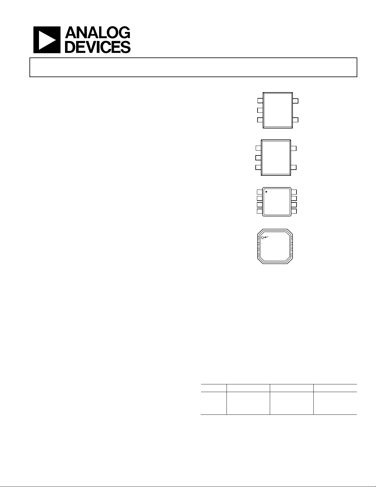
PIN CONFIGURATION
1
OUT
ADA4051-1
V–
2
TOP VIEW
(Not to Scale)
+IN
3
Figure 1. 5-Lead SOT-23 (RJ-5)
1
+IN
ADA4051-1
V–
2
TOP VIEW
(Not to Scale)
–IN
3
Figure 2. 5-Lead SC-70 (KS-5)
OUT A
1
ADA4051-2
2
–IN A
+IN A
V–
TOP VIEW
3
(Not to Scale)
4
Figure 3. 8-Lead MSOP (RM-8)
5
4
8
7
6
5
5
4
V+
OUT
V+
OUT B
–IN B
+IN B
V+
–IN
08056-064
08056-066
08056-001
GENERAL DESCRIPTION
The ADA4051-1/ADA4051-2 are CMOS, micropower, zerodrift operational amplifiers utilizing an innovative chopping
technique. These amplifiers feature rail-to-rail input/output
swing and extremely low offset voltage while operating from a
1.8 V to 5.5 V power supply. In addition, these amplifiers offer
high power supply rejection ratio (PSRR) and common-mode
rejection ratio (CMRR) while operating with a typical supply
current of 13 μA per amplifier. This combination of features
makes the ADA4051-1/ADA4051-2 amplifiers ideal choices for
battery-powered applications where high precision and low
power consumption are important.
PIN 1
1OUT A
INDICATOR
2–IN A
ADA4051-2
3+IN A
TOP VIEW
(Not to Scale)
4V–
NOTES
1. IT IS RE COMMENDED THAT THE
EXPOSED PAD BE CO NNE CTED TO V–.
8V+
7OUT B
6 –IN B
5 +IN B
08056-065
Figure 4. 8-Lead LFCSP (CP-8-2)
The ADA4051-1/ADA4051-2 are specified for the extended
industrial temperature range of −40°C to +125°C. The ADA4051-1
amplifier is available in 5-lead SOT-23 and 5-lead SC-70 packages.
The ADA4051-2 amplifier is available in 8-lead MSOP and 8-lead
LFCSP packages.
The ADA4051-1/ADA4051-2 are members of a growing series
of zero-drift op amps offered by Analog Devices, Inc. Refer to
Table 1 for a list of these devices.
Table 1. Op Amps
Supply Low Power, 5 V 5 V 16 V
Single AD8538 AD8628 AD8638
Dual AD8539 AD8629 AD8639
Quad AD8630
Rev. B
Information furnished by Analog Devices is believed to be accurate and reliable. However, no
responsibility is assumed by Analog Devices for its use, nor for any infringements of patents or other
rights of third parties that may result from its use. Specifications subject to change without notice. No
license is granted by implication or otherwise under any patent or patent rights of Analog Devices.
Trademarks and registered trademarks are the property of their respective owners.
One Technology Way, P.O. Box 9106, Norwood, MA 02062-9106, U.S.A.
Tel: 781.329.4700 www.analog.com
Fax: 781.461.3113 ©2009–2010 Analog Devices, Inc. All rights reserved.

ADA4051-1/ADA4051-2
TABLE OF CONTENTS
Features .............................................................................................. 1
Applications ....................................................................................... 1
Pin Configuration ............................................................................. 1
General Description ......................................................................... 1
Revision History ............................................................................... 2
Specifications ..................................................................................... 3
Electrical Characteristics—1.8 V Operation ............................ 3
Electrical Characteristics—5 V Operation................................ 4
Absolute Maximum Ratings ............................................................ 5
REVISION HISTORY
1/10—Rev. A to Rev. B
Added ADA4051-1, 5-Lead SC-70 Package .................... Universal
Added Figure 2; Renumbered Sequentially .................................. 1
Changes to Figure 4 and General Description Section ............... 1
Changes to Electrical Characteristics—1.8 V Operation Section
and Table 2 ......................................................................................... 3
Changes to Electrical Characteristics—5 V Operation Section
and Table 3 ......................................................................................... 4
Changes to Table 5 ............................................................................ 5
Updated Outline Dimensions ....................................................... 17
Changes to Ordering Guide .......................................................... 18
10/09—Rev. 0 to Rev. A
Added ADA4051-1, 5-Lead SOT-23 Package ................. Universal
Added ADA4051-2, 8-Lead LFCSP Package .................. Universal
Changes to the Features and General Description Section,
Added Figure 1 and Figure 3 ........................................................... 1
Moved Electrical Characteristics—1.8 V Operation Section .... 3
Changes to Offset Voltage Parameter and Supply Current per
Amplifier Parameter, Table 2 .......................................................... 3
Moved Electrical Characteristics—5 V Operation Section ........ 4
Changes to Offset Voltage Parameter and Supply Current per
Amplifier Parameter, Table 2 .......................................................... 4
Changes to Thermal Resistance Section and Table 5 ................... 5
Changes to Figure 22 and Figure 25 ............................................... 9
Changes to Theory of Operation Section .................................... 15
Updated Outline Dimensions ....................................................... 17
Changes to Ordering Guide .......................................................... 18
7/09—Revision 0: Initial Version
Thermal Resistance .......................................................................5
Power Sequencing .........................................................................5
ESD Caution...................................................................................5
Typical Performance Characteristics ..............................................6
Theory of Operation ...................................................................... 15
Input Voltage Range ................................................................... 16
Output Phase Reversal ............................................................... 16
Outline Dimensions ....................................................................... 17
Ordering Guide .......................................................................... 18
Rev. B | Page 2 of 20

ADA4051-1/ADA4051-2
SPECIFICATIONS
ELECTRICAL CHARACTERISTICS—1.8 V OPERATION
VSY = 1.8 V, VCM = VSY/2 V, TA = 25°C, RL = 100 kΩ to GND, unless otherwise noted.
Table 2.
Parameter Symbol Test Conditions/Comments Min Typ Max Unit
INPUT CHARACTERISTICS
Offset Voltage VOS
ADA4051-2 0 V ≤ VCM ≤ 1.8 V 2 15 μV
ADA4051-1 0 V ≤ VCM ≤ 1.8 V 2 17 μV
Offset Voltage Drift ∆VOS/∆T −40°C ≤ TA ≤ +125°C 0.02 0.1 μV/°C
Input Bias Current IB 5 50 pA
−40°C ≤ TA ≤ +125°C 200 pA
Input Offset Current IOS 10 100 pA
−40°C ≤ TA ≤ +125°C 150 pA
Input Voltage Range −40°C ≤ TA ≤ +125°C 0 1.8 V
Common-Mode Rejection Ratio CMRR 0 V ≤ VCM ≤ 1.8 V 105 125 dB
−40°C ≤ TA ≤ +125°C 100 dB
Large-Signal Voltage Gain AVO
= 10 kΩ to VCM,
R
L
0.1 V ≤ V
≤ VSY − 0.1 V
OUT
−40°C ≤ TA ≤ +125°C 100 dB
Input Resistance RIN 8 MΩ
Input Capacitance, Differential Mode C
Input Capacitance, Common Mode C
2 pF
INDM
5 pF
INCM
OUTPUT CHARACTERISTICS
Output Voltage High VOH R
= 100 kΩ to VCM 1.796 1.799 V
L
−40°C ≤ TA ≤ +125°C 1.79 V
R
= 10 kΩ to VCM 1.76 1.796 V
L
−40°C ≤ TA ≤ +125°C 1.7 V
Output Voltage Low VOL R
= 100 kΩ to VCM 1 3 mV
L
−40°C ≤ TA ≤ +125°C 9 mV
R
= 10 kΩ to VCM 3 20 mV
L
−40°C ≤ TA ≤ +125°C 40 mV
Short-Circuit Current ISC V
Closed-Loop Output Impedance Z
f = 1 kHz, G = 10 1 Ω
OUT
= VSY or GND 13 mA
OUT
POWER SUPPLY
Power Supply Rejection Ratio PSRR 1.8 V ≤ VSY ≤ 5.5 V 110 135 dB
−40°C ≤ TA ≤ +125°C 106 dB
Supply Current per Amplifier ISY
ADA4051-2 V
ADA4051-1 V
= VSY/2 13 17 μA
OUT
= VSY/2 15 18 μA
OUT
−40°C ≤ TA ≤ +125°C 20 μA
DYNAMIC PERFORMANCE
Slew Rate SR+ RL = 10 kΩ, CL = 100 pF, G = 1 0.04 V/μs
SR− RL = 10 kΩ, CL = 100 pF, G = 1 0.03 V/μs
Settling Time tS
To 0.1%, V
R
= 10 kΩ, CL = 100 pF
L
= 1 V p-p,
IN
Gain Bandwidth Product GBP CL = 100 pF, G = 1 115 kHz
Phase Margin ΦM C
= 100 pF, G = 1 40 Degrees
L
Channel Separation CS VIN = 1.7 V, f = 100 Hz 140 dB
NOISE PERFORMANCE
Voltage Noise en p-p f = 0.1 Hz to 10 Hz 1.96 μV p-p
Voltage Noise Density en f = 1 kHz 95 nV/√Hz
Current Noise Density in f = 1 kHz 100 fA/√Hz
Rev. B | Page 3 of 20
106 130 dB
120 μs

ADA4051-1/ADA4051-2
ELECTRICAL CHARACTERISTICS—5 V OPERATION
VSY = 5.0 V, VCM = VSY/2 V, TA = 25°C, RL = 100 kΩ to GND, unless otherwise noted.
Table 3.
Parameter Symbol Test Conditions/Comments Min Typ Max Unit
INPUT CHARACTERISTICS
Offset Voltage VOS
ADA4051-2 0 V ≤ VCM ≤ 5 V 2 15 μV
ADA4051-1 0 V ≤ VCM ≤ 5 V 2 17 μV
Offset Voltage Drift ∆VOS/∆T −40°C ≤ TA ≤ +125°C 0.02 0.1 μV/°C
Input Bias Current IB 20 70 pA
−40°C ≤ TA ≤ +125°C 200 pA
Input Offset Current IOS 40 100 pA
−40°C ≤ TA ≤ +125°C 150 pA
Input Voltage Range −40°C ≤ TA ≤ +125°C 0 5 V
Common-Mode Rejection Ratio CMRR 0 V ≤ VCM ≤ 5 V 110 135 dB
−40°C ≤ TA ≤ +125°C 106 dB
Large-Signal Voltage Gain AVO
= 10 kΩ to VCM,
R
L
0.1 V ≤ V
≤ VSY − 0.1 V
OUT
−40°C ≤ TA ≤ +125°C 106 dB
Input Resistance RIN 8 MΩ
Input Capacitance, Differential Mode C
Input Capacitance, Common Mode C
2 pF
INDM
5 pF
INCM
OUTPUT CHARACTERISTICS
Output Voltage High VOH R
= 100 kΩ to VCM 4.996 4.998 V
L
−40°C ≤ TA ≤ +125°C 4.985 V
R
= 10 kΩ to VCM 4.96 4.99 V
L
−40°C ≤ TA ≤ +125°C 4.9 V
Output Voltage Low VOL R
= 100 kΩ to VCM 1 4 mV
L
−40°C ≤ TA ≤ +125°C 13 mV
R
= 10 kΩ to VCM 9 30 mV
L
−40°C ≤ TA ≤ +125°C 90 mV
Short-Circuit Current ISC V
Closed-Loop Output Impedance Z
f = 1 kHz, G = 10 1 Ω
OUT
= VSY or GND 15 mA
OUT
POWER SUPPLY
Power Supply Rejection Ratio PSRR 1.8 V ≤ VSY ≤ 5.5 V 110 135 dB
−40°C ≤ TA ≤ +125°C 106 dB
Supply Current per Amplifier ISY
ADA4051-2 V
ADA4051-1 V
= VSY/2 13 17 μA
OUT
= VSY/2 15 18 μA
OUT
−40°C ≤ TA ≤ +125°C 20 μA
DYNAMIC PERFORMANCE
Slew Rate SR+ RL = 10 kΩ, CL = 100 pF, G = 1 0.06 V/μs
SR− RL = 10 kΩ, CL = 100 pF, G = 1 0.04 V/μs
Settling Time tS
To 0.1%, V
R
= 10 kΩ, CL = 100 pF
L
= 1 V p-p,
IN
Gain Bandwidth Product GBP CL = 100 pF, G = 1 125 kHz
Phase Margin ΦM C
= 100 pF, G = 1 40 Degrees
L
Channel Separation CS VIN = 4.99 V, f = 100 Hz 140 dB
NOISE PERFORMANCE
Voltage Noise en p-p f = 0.1 Hz to 10 Hz 1.96 μV p-p
Voltage Noise Density en f = 1 kHz 95 nV/√Hz
Current Noise Density in f = 1 kHz 100 fA/√Hz
Rev. B | Page 4 of 20
115 135 dB
110 μs
ADA4051-1/ADA4051-2
ABSOLUTE MAXIMUM RATINGS
Table 4.
Parameter Rating
Supply Voltage 6 V
Input Voltage ±VSY ± 0.3 V
Input Current1 ±10 mA
Differential Input Voltage2 ±VSY
Output Short-Circuit Duration to GND Indefinite
Storage Temperature Range −65°C to +150°C
Operating Temperature Range −40°C to +125°C
Junction Temperature Range −65°C to +150°C
Lead Temperature (Soldering, 60 sec) 300°C
1
The input pins have clamp diodes to the power supply pins. Limit the input
current to 10 mA or less whenever input signals exceed the power supply
rail by 0.3 V.
2
Inputs are protected against high differential voltages by internal series
1.33 kΩ resistors and back-to-back diode-connected N-MOSFETs (with a
typical VT of 0.7 V for VCM of 0 V).
Stresses above those listed under Absolute Maximum Ratings
may cause permanent damage to the device. This is a stress
rating only; functional operation of the device at these or any
other conditions above those indicated in the operational
section of this specification is not implied. Exposure to absolute
maximum rating conditions for extended periods may affect
device reliability.
THERMAL RESISTANCE
θJA is specified for the worst-case conditions, that is, a device
soldered on a circuit board for surface-mount packages with its
exposed paddle soldered to a pad, if applicable. Tabl e 5 shows
simulated thermal values for a 4-layer (2S2P) JEDEC standard
thermal test board, unless otherwise specified.
Table 5. Thermal Resistance
Package Type θJA θ
5-Lead SOT-23 (RJ-5) 190 92 °C/W
5-Lead SC-70 (KS-5) 534 173 °C/W
8-Lead MSOP (RM-8) 142 45 °C/W
8-Lead LFCSP (CP-8-2) 77 14 °C/W
Unit
JC
POWER SEQUENCING
The op amp supplies must be established simultaneously with
or before any input signals are applied. If this is not possible, the
input current must be limited to 10 mA.
ESD CAUTION
Rev. B | Page 5 of 20
ADA4051-1/ADA4051-2
TYPICAL PERFORMANCE CHARACTERISTICS
TA = 25°C, unless otherwise noted.
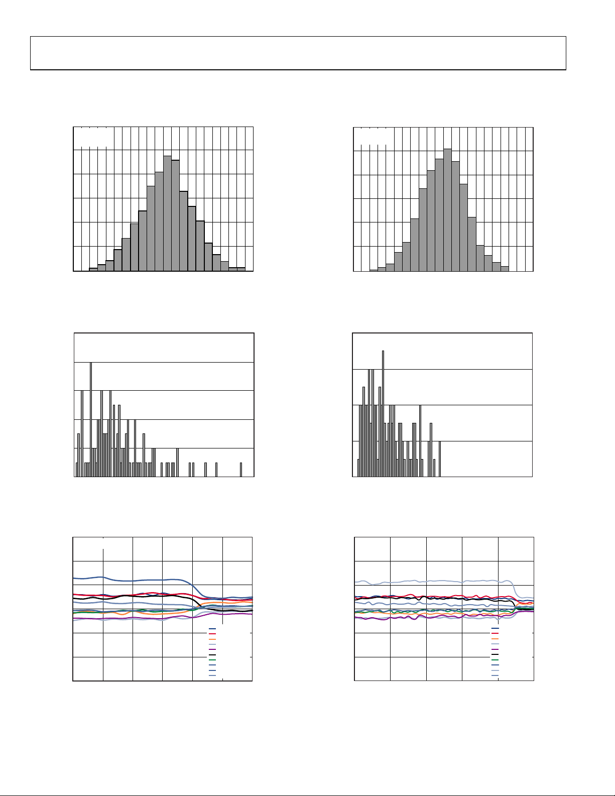
300
250
VSY = 1.8V
V
= VSY/2
CM
300
250
VSY = 5V
V
= VSY/2
CM
200
150
100
NUMBER OF AMPLIF IERS
50
0
–10–8–6–4–20246810
VOS (µV)
Figure 5. Input Offset Voltage Distribution Figure 8. Input Offset Voltage Distribution
NUMBER OF AMPLIF IERS
10
8
6
4
2
= 1.8V
V
SY
–40°C T
+125°C
A
200
150
100
NUMBER OF AMPLIFI ERS
50
0
–10–8–6–4–20246810
08056-002
8
6
4
NUMBER OF AMPLIF IERS
2
VOS (µV)
–40°C T
VSY = 5V
125°C
A
08056-005
0
0 0.01 0.02 0.03 0.04 0.05 0.06 0.07 0.08 0.09 0.10
TCVOS (µV/°C)
Figure 6. Input Offset Voltage Drift Distribution with Temperature
15
VSY = 1.8V
10
5
(µV)
0
OS
V
–5
–10
–15
0 0.3 0.6 0.9 1.2 1.5 1.8
VCM (V)
DEVICE 1
DEVICE 2
DEVICE 3
DEVICE 4
DEVICE 5
DEVICE 6
DEVICE 7
DEVICE 8
DEVICE 9
DEVICE 10
Figure 7. Input Offset Voltage vs. Input Common-Mode Voltage
08056-003
08056-004
Rev. B | Page 6 of 2
0
0 0.010.020.030.040.050.060.070.080.090.10
TCVOS (µV/°C)
Figure 9. Input Offset Voltage Drift Distribution with Temperature
15
= 5V
V
SY
10
5
(µV)
0
OS
V
–5
–10
–15
012345
(V)
V
CM
DEVICE 1
DEVICE 2
DEVICE 3
DEVICE 4
DEVICE 5
DEVICE 6
DEVICE 7
DEVICE 8
DEVICE 9
DEVICE 10
Figure 10. Input Offset Voltage vs. Input Common-Mode Voltage
0
08056-006
6-007
0805

ADA4051-1/ADA4051-2
T
TA = 25°C, unless otherwise noted.
100
80
VSY = 1.8V
I
B+
I
B–
100
VSY = 5V
80
I
B+
I
B–
60
40
(pA)
B
I
20
0
–20
25 50 75 100 125
TEMPERATURE (°C)
08056-008
Figure 11. Input Bias Current vs. Temperature
200
VSY = 1.8V
150
100
50
0
(pA)
B
I
–50
, 25°C
I
–100
–150
–200
0 0.3 0.6 0.9 1.2 1.5 1.8
V
(V)
CM
B+
I
B–
I
B+
I
B–
I
B+
I
B–
, 25°C
, 85°C
, 85°C
, 125°C
, 125°C
08056-009
Figure 12. Input Bias Current vs. Common-Mode Voltage and Temperature
60
40
(pA)
B
I
20
0
–20
25 50 75 100 125
TEMPERATURE (°C)
8056-011
Figure 14. Input Bias Current vs. Temperature
400
VSY = 5V
300
200
100
0
(pA)
B
I
–100
I
, 25°C
–200
–300
–400
0 0. 5 1.0 1.5 2.0 2.5 3.0 3. 5 4.0 4.5 5.0
VCM (V)
B+
I
B–
I
B+
I
B–
I
B+
I
B–
, 25°C
, 85°C
, 85°C
, 125°C
, 125°C
8056-012
Figure 15. Input Bias Current vs. Common-Mode Voltage and Temperature
10,000
VSY = 1.8V
1000
100
) TO SUPPLY RAIL (mV)
10
OH
1
AGE (V
0.1
OUTPUT VOL
0.01
0.001 0.01 0.1 1 10
LOAD CURRENT (mA)
–40°C
+25°C
+85°C
+125°C
Figure 13. Output Voltage (VOH) to Supply Rail vs. Load Current
and Temperature
08056-010
10,000
VSY = 5V
1000
100
) TO SUPPLY RAIL (mV)
10
OH
1
0.1
OUTPUT VOLTAGE (V
0.01
0.001 0.01 0.1 1 10010
LOAD CURRENT (mA)
–40°C
+25°C
+85°C
+125°C
Figure 16. Output Voltage (VOH) to Supply Rail vs. Load Current
and Temperature
8056-013
Rev. B | Page 7 of 2
0

ADA4051-1/ADA4051-2
TA = 25°C, unless otherwise noted.
10,000
VSY = 1.8V
1000
100
) TO SUPPLY RAIL (mV)
10
OL
1
0.1
TPUT VOLTAGE (V
OU
0.01
0.001 0.01 0.1 1 10 100
LOAD CURRENT (mA)
–40°C
+25°C
+85°C
+125°C
Figure 17. Output Voltage (VOL) to Supply Rail vs. Load Current
and Temperature
1800
1799
] (mV)
1798
OH
1797
1796
OUTPUT VOLTAGE [V
1795
V
= 1.8V
SY
= VSY/2
V
CM
1794
–40 –25 –10 5 20 35 50 65 80 95 110 125
R
RL = 100k
= 10k
L
TEMPERATURE (° C)
Figure 18. Output Voltage (VOH) vs. Temperature
10,000
VSY= 5V
1000
100
) TO SUPPLY RAIL (mV)
10
OL
1
0.1
OUTPUT VOLTAGE (V
0.01
0.001 0.01 0.1 1 10 100
8056-014
LOAD CURRENT (mA)
–40°C
+25°C
+85°C
+125°C
08056-017
Figure 20. Output Voltage (VOL) to Supply Rail vs. Load Current
and Temperature
5000
4998
4996
] (mV)
4994
OH
4992
4990
4988
4986
OUTPUT VOLTAGE [V
4984
4982
08056-015
= 5V
V
SY
V
= VSY/2
CM
–40 –25 –10 5 20 35 50 65 80 95 110 125
R
RL = 100k
= 10k
L
TEMPERATURE (° C)
08056-018
Figure 21. Output Voltage (VOH) vs. Temperature
14
= 1.8V
V
SY
V
= VSY/2
CM
12
10
] (mV)
OL
8
6
4
OUTPUT VOLTAGE [V
2
0
–40 –25 –10 5 20 35 50 65 80 95 110 125
R
= 10k
L
RL = 100k
TEMPERATURE (° C)
Figure 19. Output Voltage (VOL) vs. Temperature
08056-016
Rev. B | Page 8 of 20
14
= 5V
V
SY
V
= VSY/2
CM
12
10
] (mV)
OL
8
6
4
OUTPUT VOLTAGE [V
2
0
–40 –25 –10 5 20 35 50 65 80 95 110 125
RL = 10k
= 100k
R
L
TEMPERATURE (° C)
Figure 22. Output Voltage (VOL) vs. Temperature
6-019
0805

ADA4051-1/ADA4051-2
(
TA = 25°C, unless otherwise noted.
30
ADA4051-2
ADA4051-1
25
µA)
20
15
10
TOTAL SUPPLY CURRENT
5
0
0 0.5 1.0 1.5 2.0 2.5 3.0 3.5 4.0 4.5 5.0
SUPPLY VOLTAGE (V)
Figure 23. Total Supply Current vs. Supply Voltage Figure 26. Total Supply Current vs. Temperature
80
60
40
20
0
–20
OPEN-LOOP GAIN (dB)
GAIN
PHASE
VCM = VSY/2
VSY = 1.8V
C
= 100pF
L
180
135
90
45
0
–45
30
VCM = VSY/2
25
20
15
10
TOTAL SUPPLY CURRENT (µA)
5
0
–40 –25 –10 5 20 35 50 65 80 95 110 125
08056-020
80
60
40
20
0
PHASE (Degrees)
–20
OPEN-LOOP GAIN (dB)
TEMPERATURE (°C)
GAIN
ADA4051-2, 1.8V
ADA4051-2, 5V
ADA4051-1, 1.8V
ADA4051-1, 5V
VSY = 5V
C
= 100pF
L
PHASE
180
135
90
45
0
–45
08056-023
PHASE (Degrees)
–40
–60
100 1k 10k 100k 1M
FREQUENCY (Hz)
Figure 24. Open-Loop Gain and Phase vs. Frequency
50
40
30
20
10
0
–10
–20
CLOSED-LOOP GAIN (dB)
–30
G = 1
–40
G = 10
G = 100
–50
100 1k 10k 100k 1M
FREQUENCY ( Hz)
Figure 25. Closed-Loop Gain vs. Frequency
VSY = 1.8V
= 10k
R
L
C
= 50pF
L
–90
–135
–40
–60
100 1k 10k 100k 1M
08056-022
FREQUENCY (Hz)
–90
–135
08056-025
Figure 27. Open-Loop Gain and Phase vs. Frequency
50
40
30
20
10
0
–10
–20
CLOSED-LOOP GAIN (dB)
–30
G = 1
–40
G = 10
G = 100
–50
100 1k 10k 100k 1M
08056-061
FREQUENCY (Hz)
VSY = 5V
= 10k
R
L
= 50pF
C
L
-062
8056
Figure 28. Closed-Loop Gain vs. Frequency
Rev. B | Page 9 of 20

ADA4051-1/ADA4051-2
TA = 25°C, unless otherwise noted.
10k
VSY = 1.8V
10k
VSY = 5V
1k
100
()
OUT
Z
10
1
0.1
1k 10k 100k 1M
FREQUENCY ( Hz)
Figure 29. Output Impedance vs. Frequency
110
100
90
80
70
CMRR (dB)
60
G = 1
G = 10
G = 100
VSY = 1.8V
1k
100
()
OUT
Z
10
1
G = 1
G = 10
0.1
1k 10k 100k 1M
08056-026
FREQUENCY ( Hz)
G = 100
08056-029
Figure 32. Output Impedance vs. Frequency
110
100
90
80
70
CMRR (dB)
60
VSY = 5V
50
40
10 100 1k 10k 100k 1M
FREQUENCY ( Hz)
Figure 30. CMRR vs. Frequency
120
100
80
60
PSRR (dB)
40
20
0
100 1k 10k 100k 1M
PSRR+
PSRR–
FREQUENCY ( Hz)
VSY = 1.8V
Figure 31. PSRR vs. Frequency
50
40
10 100 1k 10k 100k 1M
08056-027
FREQUENCY (Hz)
08056-030
Figure 33. CMRR vs. Frequency
120
100
80
60
PSRR (dB)
40
20
0
100 1k 10k 100k 1M
08056-028
PSRR+
PSRR–
FREQUENCY ( Hz)
VSY = 5V
6-0310805
Figure 34. PSRR vs. Frequency
Rev. B | Page 10 of 20

ADA4051-1/ADA4051-2
TA = 25°C, unless otherwise noted.
60
= ±0.9V
V
SY
V
= 50mV p-p
IN
R
= 10k
L
C
= 50pF
50
L
40
30
OVERSHOOT (%)
20
OVERSHOOT
10
0
10 100
LOAD CAPACITANCE (pF)
+OVERSHOOT
Figure 35. Small-Signal Overshoot vs. Load Capacitance
VSY = 1.8V
= 10k
R
L
= 100pF
C
L
G = 1
= 1.5V p-p
V
IN
60
VSY = ±2.5V
V
= 50mV p-p
IN
R
= 10k
L
50
C
= 50pF
L
40
30
OVERSHOOT (%)
20
10
0
10
08056-032
LOAD CAPACITANCE (pF)
OVERSHOOT
+OVERSHOOT
100
08056-035
Figure 38. Small-Signal Overshoot vs. Load Capacitance
VSY = 5V
R
= 10k
L
C
= 100pF
L
G = 1
V
= 4V p-p
IN
VOLTAGE (500mV/DIV)
TIME (100µ s/DIV)
Figure 36. Large-Signal Transient Response
VOLTAGE (10mV/DIV)
TIME (100µ s/DIV)
Figure 37. Small-Signal Transient Response
VSY = 1.8V
= 10k
R
L
= 100pF
C
L
G = 1
= 50mV p-p
V
IN
VOLTAGE (1V/DIV)
08056-033
TIME (100µs/DIV)
8056-036
Figure 39. Large-Signal Transient Response
VSY = 5V
R
= 10k
L
C
= 100pF
L
G = 1
V
= 50mV p-p
IN
VOLTAGE (10mV/DIV)
08056-034
TIME ( 100µs/DIV)
6-037
0805
Figure 40. Small-Signal Transient Response
Rev. B | Page 11 of 20

ADA4051-1/ADA4051-2
TA = 25°C, unless otherwise noted.
VSY = 1.8V
INPUT VOLTAGE NOISE (0.5µV/DIV)
1.94µV p-p
TIME (4s/ DIV)
08056-038
VSY = 5V
1.96µV p-p
INPUT VOLTAGE NOISE (0.5µV/DIV)
TIME (4s/DIV)
Figure 41. Input Voltage Noise, 0.1 Hz to 10 Hz Figure 44. Input Voltage Noise, 0.1 Hz to 10 Hz
1k
100
10
VSY = 1.8V
1k
V
= 5V
SY
Hz)
100
10
08056-041
VOLTAGE NOISE DENSITY (nV/Hz)
1
10 100 1k 10k
FREQUENCY ( Hz)
Figure 42. Voltage Noise Density vs. Frequency
0.15
0.10
0.05
0
–0.05
INPUT VOLTAGE (50mV/DIV)
TIME (40µ s/DIV)
INPUT VOLTAGE
OUTPUT VO LTAGE
Figure 43. Positive Overload Recovery
VSY = ±0.9V
G = –10
0.5
0
–0.5
–1.0
–1.5
VOLTAGE NOISE DENSITY (nV/
1
10 100 1k 10k
08056-039
FREQUENCY ( Hz)
08056-042
Figure 45. Voltage Noise Density vs. Frequency
0.4
0.3
0.2
0.1
0
–0.1
OUTPUT VO LTAGE (500mV/DIV)
08056-040
INPUT VO LTAGE ( 100mV/DIV)
TIME (40µ s/DIV)
VSY = ±2.5V
G = –10
INPUT VOLTAGE
OUTPUT VOLTAGE
1
0
–1
OUTPUT VOLT AGE (1V/DIV)
–2
–3
08056-043
Figure 46. Positive Overload Recovery
Rev. B | Page 12 of 20

ADA4051-1/ADA4051-2
TA = 25°C, unless otherwise noted.
0.05
–0.05
0
INPUT VOLTAGE
–0.1
0.1
0
INPUT VOLTAGE
INPUT VOLTAGE (50mV/DIV)
–0.10
–0.15
INPUT VO LTAGE ( 500mV/DIV)
OUTPUT VOLTAGE
VSY = ±0.9V
G = –10
TIME (40µ s/DIV)
Figure 47. Negative Overload Recovery
INPUT VOLTAGE
ERROR
BAND
TIME (40µ s/DIV)
Figure 48. Positive Settling Time to 0.1%
OUTPUT VO LTAGE
VSY = ±0.9V
= 1V p-p
V
IN
= 10k
R
L
C
= 100pF
L
5
0
–5
1.5
1.0
0.5
0
–0.5
–0.2
–0.3
–0.4
OUTPUT V OLTAGE (500mV/DIV)
08056-044
INPUT VOLTAGE (100mV/DIV)
VSY = ±2.5V
G = –10
OUTPUT VO LTAGE
TIME (40µs/DIV)
4
3
2
1
OUTPUT VOLTAGE (1V/DIV)
0
–1
08056-047
Figure 50. Negative Overload Recovery
INPUT VOLTAGE
5
ERROR
BAND
OUTPUT VOLTAGE (5mV/ DIV)
08056-045
INPUT VO LTAGE ( 500mV/DIV)
TIME (40µ s/DIV)
OUTPUT VOLTAGE
VSY = ±2.5V
= 1V p-p
V
IN
= 10k
R
L
C
= 100pF
L
0
–5
OUTPUT VOLTAGE (5mV/ DIV)
08056-048
Figure 51. Positive Settling Time to 0.1%
INPUT VOLTAGE
5
ERROR
BAND
INPUT VO LTAGE ( 500mV/DIV)
TIME (40µs/DIV)
OUTPUT VOL TAGE
VSY = ±0.9V
V
= 1V p-p
IN
R
= 10k
L
C
= 100pF
L
0
–5
OUTPUT VOLTAGE (5mV/ DIV)
08056-046
Figure 49. Negative Settling Time to 0.1%
ERROR
BAND
INPUT VOLTAGE (500mV/DIV)
TIME (40µs/DIV)
Figure 52. Negative Settling Time to 0.1%
INPUT VOLTAGE
OUTPUT VO LTAGE
= ±2.5V
V
SY
= 1V p-p
V
IN
= 10k
R
L
C
= 100pF
L
5
0
–5
OUTPUT VOLTAGE (5mV/DIV)
08056-049
Rev. B | Page 13 of 20

ADA4051-1/ADA4051-2
–
–
R
A
R
A
TA = 25°C, unless otherwise noted.
100
–110
TION (dB)
–120
–130
CHANNEL SEPA
–140
–150
20 200 2k 20k
100k
1k
FREQUENCY (Hz)
Figure 53. Channel Separation vs. Frequency
1.8
1.5
1.2
0.9
V
= 0.5V
IN
V
= 1V
IN
V
= 1.7V
IN
VSY = 1.8V
G = –100
= 10k
R
L
C
= 50pF
L
100
–110
TION (dB)
–120
–130
CHANNEL SEPA
–140
–150
20 200 2k 20k
8056-050
100k
1k
FREQUENCY ( Hz)
VIN = 1V
V
= 3V
IN
V
= 4.99V
IN
VSY = 5V
G = –100
R
= 10k
L
C
= 50pF
L
08056-053
Figure 56. Channel Separation vs. Frequency
6
5
4
3
0.6
OUTPUT SWING (V)
VSY = 1.8V
V
= 1.7V
0.3
IN
G = 1
R
= 10k
L
C = 50pF
L
0
100 1k 10k 100k
FREQUENCY ( Hz)
Figure 54. Output Swing vs. Frequency
VSY = ±0.9V
G = 1
R
= NO LOAD
L
C
= NO LOAD
L
VOLTAG E (500mV/DIV)
V
OUT
V
IN
TIME (200µ s/DIV)
Figure 55. No Phase Reversal
8056-051
08056-052
2
OUTPUT SWING (V)
VSY = 5V
V
= 4.9V
IN
1
G = 1
R
= 10k
L
C
= 50pF
L
0
100 1k 10k 100k
FREQUENCY (Hz)
Figure 57. Output Swing vs. Frequency
VSY = ±2.5V
G = 1
R
= NO LOAD
L
C
= NO LOAD
L
VOLTAGE (1V/DIV)
V
OUT
V
IN
TIME (200 µs/DIV)
Figure 58. No Phase Reversal
08056-054
08056-055
Rev. B | Page 14 of
20

ADA4051-1/ADA4051-2
N
A
THEORY OF OPERATION
The ADA4051-1/ADA4051-2 micropower chopper operational
amplifiers feature a novel, patent-pending technique that suppresses offset-related ripple in a chopper amplifier. Instead of
filtering the ripple in the ac domain, this technique nulls the
amplifier’s initial offset in the dc domain, thus preventing ripple
at the overall output.
Auto-zeroing and chopping are two techniques widely used in
high precision CMOS amplifiers to achieve low offset, low offset
drift, and no 1/f noise. Each of these techniques has pros and
cons. Auto-zeroing results in more in-band noise due to aliasing
introduced by sampling. On the other hand, chopping produces
offset-related ripple because it modulates the initial offset
associated with the amplifier up to its chopping frequency.
To accomplish the best noise vs. power trade-off, the chopping
technique is the better approach when designing a low offset
amplifier because there is no increased in-band noise. It is
preferable to suppress the offset-related ripple inside a chopper
amplifier because the offset-related ripple would otherwise need
to be eliminated by an extra off-chip postfilter.
Figure 59 shows the block diagram design of the ADA4051-1/
ADA4051-2 chopper amplifiers employing a local feedback loop
called autocorrection feedback (ACFB). The main signal path
contains an input chopping switch network (CHOP1), a first
transconductance amplifier (Gm1), an output chopping switch
network (CHOP2), a second transconductance amplifier (Gm2),
and a third transconductance amplifier (Gm3). CHOP1 and
CHOP2 operate at 40 kHz of chopping frequency to modulate
the initial offset and 1/f noise from Gm1 up to the chopping
frequency. A fourth transconductance amplifier (Gm4) in the
ACFB senses the modulated ripple at the output of CHOP2,
caused by the initial offset voltage of Gm1. Then, the ripple is
demodulated down to a dc domain through a third chopping
switch network (CHOP3), operating with the same chopping
clock as CHOP1 and CHOP2. Finally, a null transconductance
amplifier (Gm5) tries to null any dc component at the output of
Gm1 that would otherwise appear in the overall output as ripple.
A switched-capacitor notch filter (NF) functions to selectively
suppress the undesired offset-related ripple without disturbing
the desired input signal from the overall input. The desired input
dc signal appears as a dc signal at the output of CHOP2. Then,
the initial offset is modulated up to the chopping frequency by
CHOP3 and filtered out by the NF. Therefore, initial offset does
not create any feedback and does not disturb the desired input
signal. The NF is synchronized with the chopping clock to filter
out the modulated component. In the same manner, the offset
of Gm5 is filtered out by the combination of CHOP3 and the
NF, enabling accurate ripple sensing at the output of CHOP2.
In parallel with the high dc gain path, a feedforward transconductance amplifier (Gm6) is added to bypass the phase shift
introduced by the ACFB at the chopping frequency. Gm6 is
designed to have the same transconductance as Gm1 to avoid
pole-zero doublets. This design prevents any instability introduced
by the ACFB in the overall feedback loop.
NF
CHOP2
Gm4G m5 CHOP3
CHOP1
+I
–IN
Figure 59. ADA4051-1/ADA4051-2 Chopper Amplifiers Block Diagram
Gm1
Gm6 (= Gm1)
C2
Gm2
Gm3
OUT
C3
C1
The voltage noise density, which is equal to the thermal noise
floor dominated by the Gm1, is essentially flat from dc to the
chopping frequency because CHOP1 and CHOP2 eliminate the
1/f noise generated in Gm1 and the ACFB does not contribute
any additional noise. Although the ACFB suppresses the ripple
related to the chopping, there is a remaining voltage ripple. To
further suppress the remaining ripple down to a desired level, it
is recommended to have a postfilter at the output of the amplifier.
The remaining voltage ripple originates from two sources. The
first type of ripple is due to the residual ripple associated with
the initial offset of the Gm1. It is proportional to the magnitude
of the initial offset and creates a spectrum at the chopping
frequency (f
). When the amplifier is configured as a unity-
CHOP
gain buffer, this ripple has a typical value of 4.9 μV rms and a
maximum of 34.7 μV rms. The second type of ripple is due to
the intermodulation between the high frequency input signal
and the chopping frequency. This ripple depends on the input
frequency (f
) and creates a spectrum at frequencies equal to
IN
the difference between the chopping frequency and the input
frequency (f
− fIN), as well as at frequencies equal to the
CHOP
summation of the chopping frequency and the input frequency
(f
+ fIN). The magnitude of the ripple for different input
CHOP
frequencies is shown in Figure 60.
500
400
300
200
TED OUTPUT RIPPLE (µ V rms)
100
MODUL
0
012345678910
INPUT FREQ UENCY (kHz)
Figure 60. ADA4051-1/ADA4051-2 Modulated Output Ripple vs. Input Frequency
08056-063
08056-060
Rev. B | Page 15 of 20

ADA4051-1/ADA4051-2
The design architecture of the ADA4051-1/ADA4051-2
specifically targets precision signal conditioning applications
requiring accurate and stable performance from dc to 10 Hz
bandwidth. In summary, the main features of the ADA4051-1/
ADA4051-2 chopper amplifiers are
• Considerable suppression of the offset-related ripple
• No affect on the desired input signal as long as its
frequency is much lower than the chopping frequency
shown in Figure 60
• Achievement of low offset similar to a conventional
chopper amplifier
• No introduction of excess noise
The ADA4051-1/ADA4051-2 chopper amplifiers provide a railto-rail input range with a 1.8 V to 5.5 V supply voltage range and
20 μA supply current consumption over the −40°C to +125°C
extended industrial temperature range. The gain bandwidth is
125 kHz as a unity-gain stable amplifier up to 100 pF load
capacitance.
INPUT VOLTAGE RANGE
The ADA4051-1/ADA4051-2 have internal ESD protection diodes.
These diodes are connected between the inputs and each supply
rail to protect the input MOSFETs from an electrical discharge
event and are reversed-biased during normal operation. This
protection scheme allows voltages as high as approximately 0.3 V
beyond the supplies (±V
either terminal without causing permanent damage.
If either input exceeds one of the supply rails by more than 0.3 V,
these ESD diodes become forward-biased and large amounts of
current begin to flow through them. Without current limiting, this
excessive current would cause permanent damage to the device.
If the inputs are expected to be subject to overvoltage conditions,
install a resistor in series with each input to limit the input current
to 10 mA maximum.
± 0.3 V) to be applied at the input of
SY
The ADA4051-1/ADA4051-2 also have internal circuitry that
protects the input stage from high differential voltages. This
circuitry is composed of internal 1.33 kΩ resistors in series with
each input and back-to-back diode-connected N-MOSFET (with a
typical V
of 0.7 V for a VCM of 0 V) after these series resistors. With
T
normal negative feedback operating conditions, the ADA4051-1/
ADA4051-2 amplifiers correct their output to ensure that the two
inputs are at the same voltage. However, if the device is configured
as a comparator or there are unusual operating conditions, the
input voltages can be forced to different potentials, which may
cause excessive current to flow through the internal diodeconnected N-MOSFETs.
Although the ADA4051-1/ADA4051-2 are rail-to-rail input
amplifiers, take care to ensure that the potential difference
between the inputs does not exceed ±V
to avert permanent
SY
damage to the device.
OUTPUT PHASE REVERSAL
Although output phase reversal can occur with other amplifiers
when the input common-mode voltage range is exceeded, the
ADA4051-1/ADA4051-2 amplifiers are designed to prevent
any output phase reversal, provided both inputs are maintained
approximately within 0.3 V above and below the supply voltages
(±V
± 0.3 V).
SY
With other amplifiers, the outputs may jump in the opposite
direction to the supply rail when a common-mode voltage
moves outside the common-mode range. This usually occurs
when one of the internal stages of the amplifier no longer has
sufficient bias voltage across it and subsequently turns off.
However, with the ADA4051-1/ADA4051-2 amplifiers, if one
or both inputs exceed the input voltage range but remain within
the ±V
remains in saturation mode, without phase reversal, until the
input voltage is brought back to within the input voltage range
limits as shown in Figure 55 and Figure 58.
± 0.3 V range, an internal loop opens and the output
SY
Rev. B | Page 16 of 20

ADA4051-1/ADA4051-2
0
0
OUTLINE DIMENSIONS
3.00
2.90
2.80
.15 MAX
.05 MIN
1.70
1.60
1.50
1.30
1.15
0.90
5
123
4
1.90
BSC
0.50 MAX
0.35 MIN
COMPLIANT TO JEDEC ST ANDARDS MO-178-AA
0.95 BSC
1.45 MAX
0.95 MIN
3.00
2.80
2.60
SEATING
PLANE
0.20 MAX
0.08 MIN
10°
0.55
0.20
5°
BSC
0°
0.45
0.35
121608-A
Figure 61. 5-Lead Small Outline Transistor Package [SOT-23]
(RJ-5)
Dimensions shown in millimeters
2.20
2.00
1.80
2.40
1.35
1.25
1.15
45
2.10
1.80
312
0.65 BSC
1.00
0.90
0.70
0.10 MAX
COPLANARITY
0.10
1.10
0.80
0.30
0.15
COMPLIANT TO JEDEC STANDARDS MO-203-AA
SEATING
PLANE
0.40
0.10
0.22
0.08
0.46
0.36
0.26
072809-A
Figure 62. 5-Lead Thin Shrink Small Outline Transistor Package [SC-70]
(KS-5)
Dimensions shown in millimeters
Rev. B | Page 17 of 20

ADA4051-1/ADA4051-2
3.20
3.00
2.80
PIN 1
IDENTIFIER
0.95
0.85
0.75
0.15
0.05
COPLANARITY
0.10
3.20
3.00
2.80
8
5
5.15
4.90
4
0.40
0.25
4.65
1.10 MAX
15° MAX
6°
0°
0.23
0.09
1
0.65 BSC
COMPLIANT TO JEDEC STANDARDS MO-187-AA
0.80
0.55
0.40
100709-B
Figure 63. 8-Lead Mini Small Outline Package [MSOP]
(RM-8)
Dimensions shown in millimeters
INDICATOR
0.90 MAX
0.85 NOM
SEATING
PLANE
3.25
3.00 SQ
PIN 1
12° MAX
2.75
TOP
VIEW
0.70 MAX
0.65 TYP
0.30
0.23
0.18
2.95
2.75 SQ
2.55
0.05 MAX
0.01 NOM
0.20 REF
0.60 MAX
Figure 64. 8-Lead Lead Frame Chip Scale Package [LFCSP_VD]
3 mm × 3 mm Body, Very Thin, Dual Lead
(CP-8-2)
Dimensions shown in millimeters
0.60 MAX
5
EXPOSED
PA D
(BOTTOM VIEW)
0.50
0.40
0.30
4
FOR PROPER CONNECTION O F
THE EXPOSE D PAD, REFER T O
THE PIN CONF IGURATIO N AND
FUNCTION DESCRIPTIO NS
SECTION OF THIS DATA SHEET.
0.50
BSC
8
1.60
1.45
1.30
1
1.89
1.74
1.59
PIN 1
INDICATOR
90308-B
ORDERING GUIDE
1
Model
ADA4051-1ARJZ-R2 −40°C to +125°C 5-Lead SOT-23 RJ-5 A0U
ADA4051-1ARJZ-R7 −40°C to +125°C 5-Lead SOT-23 RJ-5 A0U
ADA4051-1ARJZ-RL −40°C to +125°C 5-Lead SOT-23 RJ-5 A0U
ADA4051-1AKSZ-R2 −40°C to +125°C 5-Lead SC-70 KS-5 A0U
ADA4051-1AKSZ-R7 −40°C to +125°C 5-Lead SC-70 KS-5 A0U
ADA4051-1AKSZ-RL −40°C to +125°C 5-Lead SC-70 KS-5 A0U
ADA4051-2ACPZ-R2 −40°C to +125°C 8-Lead LFCSP_VD CP-8-2 A2M
ADA4051-2ACPZ-R7 −40°C to +125°C 8-Lead LFCSP_VD CP-8-2 A2M
ADA4051-2ACPZ-RL −40°C to +125°C 8-Lead LFCSP_VD CP-8-2 A2M
ADA4051-2ARMZ −40°C to +125°C 8-Lead MSOP RM-8 A2M
ADA4051-2ARMZ-R7 −40°C to +125°C 8-Lead MSOP RM-8 A2M
ADA4051-2ARMZ-RL −40°C to +125°C 8-Lead MSOP RM-8 A2M
1
Z = RoHS Compliant Part.
Temperature Range Package Description Package Option Branding
Rev. B | Page 18 of 20

ADA4051-1/ADA4051-2
NOTES
Rev. B | Page 19 of 20

ADA4051-1/ADA4051-2
NOTES
©2009–2010 Analog Devices, Inc. All rights reserved. Trademarks and
registered trademarks are the property of their respective owners.
D08056-0-1/10(B)
Rev. B | Page 20 of 20
 Loading...