

–
+
1.8 nV/√Hz, 36 V Precision Amplifiers
FEATURES
Very low voltage noise: 1.8 nV/√Hz
Low input bias current: 90 nA maximum
Offset voltage: 125 μV maximum
High gain: 120 dB
Wide bandwidth: 12 MHz
±5 V to ±15 V operation
APPLICATIONS
Precision instrumentation
Filter blocks
Microphone preamplifiers
Industrial control
Thermocouples and RTDs
Reference buffers
GENERAL DESCRIPTION
The ADA4004-1/ADA4004-2/ADA4004-4 are 1.8 nV/√Hz
precision amplifiers featuring 40 μV offset, 0.7 μV/°C drift, 12
MHz bandwidth, and low 1.7 mA per amplifier supply current.
The ADA4004-1/ADA4004-2/ADA4004-4 are designed on the
high performance iPolar™ process, enabling improvements such
as reduced noise and power consumption, increased speed and
stability, and smaller footprint size. Novel design techniques enable
the ADA4004-1/ADA4004-2/ADA4004-4 to achieve 1.8 nV/√Hz
voltage noise density and a low 6 Hz 1/f noise corner frequency
while consuming just 1.7 mA per amplifier. The small package
saves board space, reduces cost, and improves layout flexibility.
Applications for these amplifiers include high precision controls,
PLL filters, high performance precision filters, medical and
analytical instrumentation, precision power supply controls,
ATE, and data acquisition systems. Operation is fully specified
from ±5 V to ±15 V from −40°C to +125°C.
The ADA4004-1, ADA4004-2, and ADA4004-4 are members
of a growing series of low noise op amps offered by Analog
Devices, Inc. (see Tab le 1).
ADA4004-1/ADA4004-2/ADA4004-4
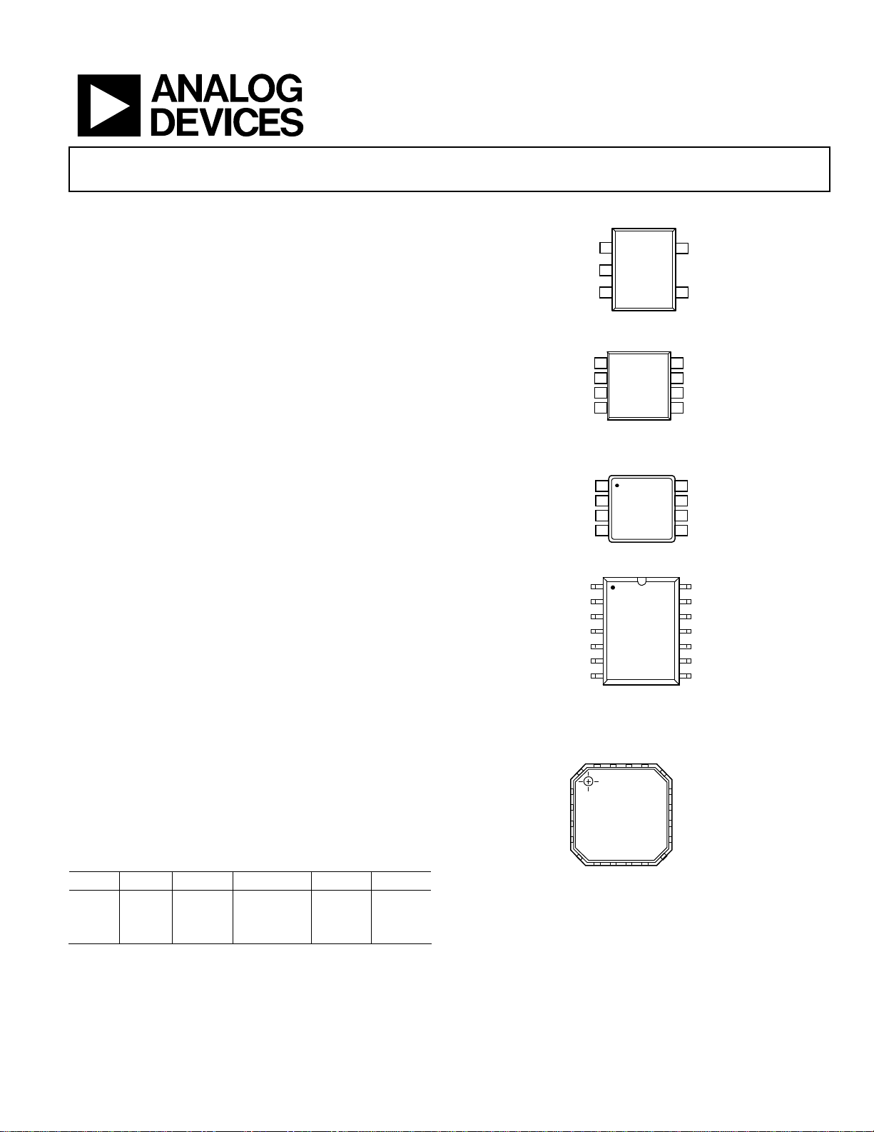
PIN CONFIGURATIONS
1
OUT
ADA4004-1
V– 2
TOP VIEW
(Not to Scale)
+IN 3
Figure 1. 5-Lead SOT
(RJ-5)
NC
1
ADA4004-1
IN
2
3
IN
TOP VIEW
(Not to Scale)
4
V–
NC = NO CONNECT
Figure 2. 8-Lead SOIC
(R-8)
OUT A
1
–IN A
+IN A
ADA4004-2
2
TOP VIEW
3
(Not to Scale)
4
V–
NC = NO CONNECT
Figure 3. 8-Lead MSOP (RM-8) and 8-Lead SOIC (R-8)
1
OUT A OUT D
2
–IN A –IN D
3
+IN A +IN D
V+ V–
+IN B +IN C
–IN B –IN C
OUT B OUT C
4
5
6
7
ADA4004-4
TOP VIEW
(Not to Scale)
Figure 4. 14-Lead SOIC
(R-14)
NC16OUT A15OUT D14NC
13
1
–IN A
ADA4004-4
2
+IN A
V+
+IN B
3
4
TOP VIEW
(Not to Scale)
V+5
–IN4
05577-001
NC
8
V+
7
6
OUT
5
NC
05577-002
V+
8
OUT B
7
6
–IN B
5
+IN B
5577-003
14
13
12
11
10
9
8
12
–IN D
11
+IN D
10
V–
9
+IN C
05577-091
Table 1. Voltage Noise
Pkg. 0.9 nV 1.1 nV 1.8 nV 2.8 nV 3.8 nV
Single AD797 AD8597 ADA4004-1 AD8675 AD8671
Dual AD8599 ADA4004-2 AD8676 AD8672
Quad ADA4004-4 AD8674
NOTES
1. NC = NO CONNECT.
2. IT IS RECOMMENDED THAT THE EXPOSED PAD
BE CONNECTED TO V–.
5
7
8
–IN B
OUT B6OUT C
–IN C
Figure 5. 16-Lead LFCSP
05577-005
(CP-16-4)
Rev. G
Information furnished by Analog Devices is believed to be accurate and reliable. However, no
responsibility is assumed by Anal og Devices for its use, nor for any infringements of patents or ot her
rights of third parties that may result from its use. Specifications subject to change without notice. No
license is granted by implication or otherwise under any patent or patent rights of Analog Devices.
Trademarks and registered trademarks are the property of their respective owners.
One Technology Way, P.O. Box 9106, Norwood, MA 02062-9106, U.S.A.
Tel: 781.329.4700 www.analog.com
Fax: 781.461.3113 ©2006–2011 Analog Devices, Inc. All rights reserved.

ADA4004-1/ADA4004-2/ADA4004-4
TABLE OF CONTENTS
Features.............................................................................................. 1
Applications....................................................................................... 1
General Description......................................................................... 1
Pin Configurations........................................................................... 1
Revision History ...............................................................................2
Specifications..................................................................................... 3
REVISION HISTORY
4/11—Rev. F to Rev. G
Changes to Figure 1.......................................................................... 1
Updated Outline Dimensions....................................................... 12
6/10—Rev. E to Rev. F
Added Differential Input Current to Table 4................................ 5
Changes to Figure 14 and Figure 17............................................... 7
10/09—Rev. D to Rev. E
Changes to Product Title, General Description Section, and
Figure 5 .............................................................................................. 1
Updated Outline Dimensions (RM-8)......................................... 13
Changes to Ordering Guide.......................................................... 14
6/09—Rev. C to Rev. D
Changes to Figure 5.......................................................................... 1
10/08—Rev. B to Rev. C
Added ADA4004-1 and ADA4004-2...............................Universal
Added 5-Lead SOT, 8-Lead SOIC, and 8-Lead MSOP .......Universal
Changes to Features Section.................................................................... 1
Added Figure 1 to Figure 3; Renumbered Sequentially......................1
Changes to General Description Section ..............................................1
Added Table 1; Renumbered Sequentially............................................ 1
Change to Output Voltage Low Parameter, Table 2............................ 3
Changes to Supply Current per Amplifier Parameter, Table 2..........3
Added Phase Margin Parameter, Table 2 ..............................................3
Change to Output Voltage Low Parameter, Table 3............................ 3
Changes to Supply Current per Amplifier Parameter, Table 3..........4
Added Phase Margin Parameter, Table 3 ..............................................4
Changes to Table 4.....................................................................................5
Changes to Thermal Resistance Section................................................5
Changes to Table 5.....................................................................................5
Update Outline Dimensions..................................................................12
Changes to Ordering Guide...................................................................13
Absolute Maximum Ratings ............................................................5
Thermal Resistance.......................................................................5
ESD Caution...................................................................................5
Typical Performance Characteristics..............................................6
Outline Dimensions....................................................................... 12
Ordering Guide .......................................................................... 14
11/07—Rev. A to Rev. B
Changed V
Changes to General Description .....................................................1
Changes to Supply Current per Amplifier .....................................3
Changes to Open-Loop Gain...........................................................4
Changes to Supply Current per Amplifier .....................................4
Changes to Figure 10, Figure 11, Figure 13, and Figure 14..........7
Changes to Figure 26.........................................................................9
Updated Outline Dimensions....................................................... 12
Changes to Ordering Guide.......................................................... 12
7/06—Rev. 0 to Rev. A
Changes to Table 4.............................................................................5
Updated Outline Dimensions....................................................... 12
Changes to Ordering Guide.......................................................... 12
1/06—Revision 0: Initial Version
to VSY..............................................................Universal
S
Rev. G | Page 2 of 16

ADA4004-1/ADA4004-2/ADA4004-4
SPECIFICATIONS
VSY = ±5 V, VCM = 0 V, TA = 25°C, unless otherwise specified.
Table 2.
Parameter Symbol Conditions Min Typ Max Unit
INPUT CHARACTERISTICS
Offset Voltage VOS 40 140 μV
−40°C ≤ T
≤ +125°C
A
Input Bias Current IB 40 85 nA
−40°C ≤ T
≤ +125°C
A
Input Offset Current IOS 40 85 nA
−40°C ≤ T
≤ +125°C
A
Input Voltage Range IVR −3.5 +3.5 V
Common-Mode Rejection Ratio CMRR VCM = −3.0 V to +3.0 V 105 111 dB
Open-Loop Gain AVO R
Offset Voltage Drift ∆VOS/∆T
−40°C ≤ T
= 2 kΩ, V
L
−40°C ≤ T
−40°C ≤ T
≤ +125°C
A
= −2.5 V to +2.5 V 250 400 V/mV
OUT
≤ +125°C
A
≤ +125°C
A
OUTPUT CHARACTERISTICS
Output Voltage High VOH R
Output Voltage Low VOL R
= 2 kΩ to ground 3.7 3.9 V
L
−40°C ≤ T
= 2 kΩ to ground −3.6 −3.55 V
L
−40°C ≤ T
≤ +125°C
A
≤ +125°C
A
Short-Circuit Limit ISC 25 mA
Output Current IO V
−40°C ≤ T
OUT
≤ +125°C
A
= ±3.6 V ±10 mA
POWER SUPPLY
Power Supply Rejection Ratio PSRR
= ±5 V to ±15 V
V
SY
−40°C ≤ T
≤ +125°C
A
Supply Current per Amplifier ISY 2.0 mA
−40°C ≤ T
≤ +125°C
A
DYNAMIC PERFORMANCE
Slew Rate SR RL = 2 kΩ to ground 2.7 V/μs
Gain Bandwidth Product GBP 12 MHz
Phase Margin ΦM 48 Degrees
NOISE PERFORMANCE
Voltage Noise e
f = 0.1 Hz to 10 Hz 0.1 μV p-p
n p-p
Voltage Noise Density en f = 1 kHz 1.8 nV/√Hz
Current Noise Density in f = 10 Hz 3.5 pA/√Hz
Current Noise Density in f = 200 Hz 1.2 pA/√Hz
300 μV
165 nA
100 nA
95 110 dB
170 V/mV
0.7 1 μV/°C
3.4 3.6 V
−3.6 −3.4 V
mA
110 118 dB
110 dB
2.2 mA
Rev. G | Page 3 of 16

ADA4004-1/ADA4004-2/ADA4004-4
VSY = ±15 V, VCM = 0 V, TA = 25°C, unless otherwise specified.
Table 3.
Parameter Symbol Conditions Min Typ Max Unit
INPUT CHARACTERISTICS
Offset Voltage VOS 40 125 μV
−40°C ≤ T
≤ +125°C
A
Input Bias Current IB 40 90 nA
−40°C ≤ T
≤ +125°C
A
Input Offset Current IOS 60 nA
−40°C ≤ T
≤ +125°C
A
Input Voltage Range IVR −12.5 +12.5 V
Common-Mode Rejection Ratio CMRR VCM = −12.5 V to +12.5 V 110 113 dB
Open-Loop Gain AVO R
Offset Voltage Drift ∆VOS/∆T
−40°C ≤ T
= 2 kΩ, V
L
−40°C ≤ T
−40°C ≤ T
≤ +125°C
A
= −12.0 V to +12.0 V 500 1200 V/mV
OUT
≤ +125°C
A
≤ +125°C
A
OUTPUT CHARACTERISTICS
Output Voltage High VOH R
Output Voltage Low VOL R
= 2 kΩ to ground 13.4 13.6 V
L
−40°C ≤ T
= 2 kΩ to ground −13.3 −13.2 V
L
−40°C ≤ T
≤ +125°C
A
≤ +125°C
A
Short-Circuit Limit ISC 25 mA
Output Current IO V
= ±13.6 V ±10 mA
OUT
POWER SUPPLY
Power Supply Rejection Ratio PSRR
= ±5 V to ±15 V
V
SY
−40°C ≤ T
≤ +125°C
A
Supply Current per Amplifier ISY 2.2 mA
−40°C ≤ T
≤ +125°C
A
DYNAMIC PERFORMANCE
Slew Rate SR RL = 2 kΩ to ground 2.7 V/μs
Gain Bandwidth Product GBP 12 MHz
Phase Margin ΦM 48 Degrees
NOISE PERFORMANCE
Voltage Noise e
f = 0.1 Hz to 10 Hz 0.15 μV p-p
n p-p
Voltage Noise Density en f = 1 kHz 1.8 nV/√Hz
Current Noise Density in f = 10 Hz 3.5 pA/√Hz
Current Noise Density in f = 200 Hz 1.2 pA/√Hz
270 μV
165 nA
100 nA
100 104 dB
250 500 V/mV
0.7 1 μV/°C
13.1 13.3 V
−13.25 −13.15 V
110 118 dB
110 dB
2.4 mA
Rev. G | Page 4 of 16
ADA4004-1/ADA4004-2/ADA4004-4
ABSOLUTE MAXIMUM RATINGS
Table 4.
Parameter Rating
Supply Voltage ±18 V or +36 V
Input Voltage V− < VIN < V+
Differential Input Voltage ±V supply
Differential Input Current ±5 mA
Output Short-Circuit Duration to GND Indefinite
Storage Temperature Range −65°C to +150°C
Operating Temperature Range −40°C to +125°C
Junction Temperature Range −65°C to +150°C
Lead Temperature (Soldering 60 sec) 300°C
Stresses above those listed under Absolute Maximum Ratings
may cause permanent damage to the device. This is a stress
rating only; functional operation of the device at these or any
other conditions above those indicated in the operational
section of this specification is not implied. Exposure to absolute
maximum rating conditions for extended periods may affect
device reliability.
THERMAL RESISTANCE
θJA is specified with the device soldered on a circuit board with
its exposed paddle soldered to a pad (if applicable) on a 4-layer
JEDEC standard printed circuit board with zero airflow.
Table 5.
Package Type θJA θ
5-Lead SOT (RJ-5) 230 92 °C/W
8-Lead SOIC (R-8), ADA4004-1 177 53 °C/W
8-Lead SOIC (R-8), ADA4004-2 155 45 °C/W
8-Lead MSOP (RM-8) 186 52 °C/W
14-Lead SOIC_N (R-14) 115 36 °C/W
16-Lead LFCSP_VQ (CP-16-4) 44 31.5 °C/W
Unit
JC
ESD CAUTION
Rev. G | Page 5 of 16

ADA4004-1/ADA4004-2/ADA4004-4
TYPICAL PERFORMANCE CHARACTERISTICS
250
200
ADA4004-4
V
= ±15V
SY
300
250
ADA4004-4
V
= ±15V
SY
150
100
NUMBER OF AMPL IFIERS
50
0
–55 –35 –15 5 25 45 65 85 105
VOS (µV)
Figure 6. Number of Amplifiers vs. Input Offset Voltage
180
160
140
120
100
80
60
NUMBER OF AMPL IFIERS
40
20
0
–30 1149882665034182–14
VOS (µV)
Figure 7. Number of Amplifiers vs. Input Offset Voltage
ADA4004-4
V
= ±5V
SY
200
150
100
NUMBER OF AMPL IFIERS
50
0
010.90. 80.70.60.50.40.30.20.1
05577-006
TCVOS (µV/°C)
Figure 9. Number of Amplifiers vs. TCV
250
200
150
100
NUMBER OF AMPL IFIERS
50
0
011.00.90.80.70.60.50. 40.30.20.1
05577-007
TCVOS (µV°C)
Figure 10. Number of Amplifiers vs. TCV
.0
05577-009
OS
ADA4004-4
V
= ±5V
SY
OS
.1
05577-010
120
80
(µV)
OS
V
40
0
–50 150100500
ADA4004-4
VSY = ±5V
V
SY
TEMPERATURE (° C)
Figure 8. Input Offset Voltage vs. Temperature
= ±15V
05577-008
Rev. G | Page 6 of 16
80
40
(nA)
B
I
0
–40
–50 150100500
ADA4004-4
= ±15V
V
= ±5V
V
SY
TEMPERATURE (° C)
SY
Figure 11. Input Bias Current vs. Temperature
05577-011

ADA4004-1/ADA4004-2/ADA4004-4
–
–
8
ADA4004-4
7
8
ADA4004-4
(mA)
SY
I
15.00
14.75
14.50
14.25
= ±15V
SY
14.00
(V) @ V
13.75
OH
V
13.50
13.25
13.00
–50 150100500
6
5
4
3
2
1
0
0330252015105
SUPPLY VOLTAGE (V)
Figure 12. Supply Current vs. Total Supply Voltage
ADA4004-4
R
V
= ±5V
SY
= ±15V
V
SY
TEMPERATURE (°C)
Figure 13. V
vs. Temperature
OH
= 2kΩ
L
7
V
6
(mA)
SY
I
5
4
5
05577-012
–50 150100500
Figure 15. Supply Current vs. Temperature
= ±15V
SY
(V) @ V
OL
V
13.00
–13.25
–13.50
–13.75
–14.00
–14.25
–14.50
–14.75
–15.00
= ±15V
V
SY
V
= ±5V
SY
–50 150100500
TEMPERATURE (°C)
5.00
4.75
4.50
4.25
4.00
3.75
3.50
3.25
3.00
= ±5V
SY
(V) @ V
OH
V
05577-013
Figure 16. V
= ±15V
SY
V
= ±5V
SY
TEMPERATURE (° C)
vs. Temperature
OL
ADA4004-4
R
= 2kΩ
L
3.00
–3.25
–3.50
–3.75
–4.00
–4.25
–4.50
–4.75
–5.00
05577-015
= ±5V
SY
(V) @ V
OL
V
05577-016
120
100
80
PHASE
60
GAIN
40
20
OPEN-LOOP GAIN (dB)
VSY = ±15V
0
BW = 15MHz
R
= 10MΩ
L
–20
C
= 20pF
L
φ
= 50°
M
–40
1k 100M10M1M100k10k
FREQUENCY (Hz)
Figure 14. Open-Loop Gain and Phase vs. Frequency
ADA4004-4
135
90
45
0
–45
120
ADA4004-4
135
100
80
PHASE
90
60
40
PHASE (°)
05577-014
20
OPEN-LOOP GAIN (dB)
VSY = ±5V
0
BW = 12.2MHz
R
–20
C
φ
–40
1k 100M10M1M100k10k
= 10MΩ
L
= 20pF
L
= 52.9°
M
GAIN
FREQUENCY (Hz)
45
0
–45
PHASE (°)
05577-017
Figure 17. Open-Loop Gain and Phase vs. Frequency
Rev. G | Page 7 of 16

ADA4004-1/ADA4004-2/ADA4004-4
1600
1200
800
V
= ±15V
SY
ADA4004-4
R
= 2kΩ
L
50
G = +100
40
30
G = +10
20
ADA4004-4
V
= ±15V
SY
OPEN-LOOP GAIN (V/mV)
400
0
–50 150100500
50
40
30
20
10
CLOSED-LOOP GAIN (dB)
0
–10
10k 100M10M1M100k
VSY = ±5V
TEMPERATURE (° C)
Figure 18. Open-Loop Gain vs. Temperature
G = +100
G = +10
G = +1
FREQUENCY (Hz)
Figure 19. Closed-Loop Gain vs. Frequency
ADA4004-4
V
= ±5V
SY
10
CLOSED-LOOP GAIN (dB)
05577-018
G = +1
0
–10
10k 100M10M1M100k
FREQUENCY (Hz)
05577-021
Figure 21. Closed-Loop Gain vs. Frequency
1k
100
G = +100
(Ω)
10
OUT
R
1
0.1
10 1k100 100M10M1M100k10k
05577-019
FREQUENCY (Hz)
G = +1
ADA4004-4
V
= ±15V
SY
G = +10
05577-022
Figure 22. Output Impedance vs. Frequency
1k
100
(Ω)
10
OUT
R
1
0.1
10 1k100 100M10M1M100k10k
Figure 20. Output Impedance vs. Frequency
G = +100
FREQUENCY (Hz)
G = +1
ADA4004-4
V
= ±5V
SY
G = +10
05577-020
Rev. G | Page 8 of 16
120
100
80
60
PSRR (dB)
40
20
0
10 1k100 10M1M100k10k
–PSRR
Figure 23. PSRR vs. Frequency
+PSRR
FREQUENCY (Hz)
ADA4004-4
VSY = ±15V, ±5V
V
= 50mV
IN
05577-023

ADA4004-1/ADA4004-2/ADA4004-4
126
122
ADA4004-4
V
= ±15V, ±5V
SY
120
100
ADA4004-4
VSY = ±15V, ±5V
V
= 50mV
IN
118
PSRR (dB)
114
110
106
–50 150100500
140
120
CMRR (dB)
100
TEMPERATURE (° C)
Figure 24. PSRR vs. Temperature
V
= ±15V
SY
= ±5V
V
SY
ADA4004-4
80
60
CMRR (dB)
40
20
0
100 10k1k 10M1M100k
05577-024
FREQUENCY (Hz)
05577-027
Figure 27. CMRR vs. Frequency
10
V
(V)
1
OUT
∆V
OL
ADA4004-4
V
SY
V
OH
= ±15V
80
–50 150100500
10
(V)
1
OUT
∆V
0.1
0.01 1001010. 1
TEMPERATURE (° C)
Figure 25. CMRR vs. Temperature
ADA4004-4
V
V
OL
V
OH
I
(mA)
LOAD
Figure 26. Output Voltage vs. Current Load
SY
= ±5V
0.1
0.01 1001010. 1
05577-025
I
LOAD
(mA)
05577-028
Figure 28. Output Voltage vs. Current Load
90
ADA4004-4
VSY = ±15V
80
V
= 1kHz
IN
70
60
50
40
OVERSHOOT (%)
30
20
10
0
05577-026
0.10.01 100101
VIN = ±50mV
±OS
C
LOAD
(nF)
VIN = ±100mV
±OS
05577-029
Figure 29. Small-Signal Overshoot vs. Capacitive Load
Rev. G | Page 9 of 16

ADA4004-1/ADA4004-2/ADA4004-4
T
60
50
ADA4004-4
VSY = ±5V
V
= ±50mV
IN
ADA4004-4
V
= ±15V
SY
C
= 1nF
L
G = +1
40
30
OVERSHOOT (%)
20
10
0
022.01.51.00. 5
–OS
+OS
CL (nF)
Figure 30. Small-Signal Overshoot vs. Capacitive Load
2
AGE (50mV/DIV)
VOL
ADA4004-4
V
= ±15V
SY
C
= 1nF
L
G = +1
2
VOLTAGE (1V/DIV)
.5
05577-030
TIME (10µ s/DIV)
Figure 33. Large-Signal Transient Response
2
VOLTAGE (50mV/DIV)
ADA4004-4
= ±5V
V
SY
= 1nF
C
L
G = +1
05577-033
TIME (100µs/DIV)
Figure 31. Small-Signal Transient Response
V
IN
V
OUT
1
VOLTAGE (2V/DIV)
TIME (400µ s/DIV)
ADA4004-4
VSY = ±15V
Figure 32. No Phase Reversal
05577-031
Figure 34. Small-Signal Transient Response
1
NOISE (50nV/DIV)
05577-032
Figure 35. Voltage Noise (0.1 Hz to 10 Hz)
TIME (100µs/DIV)
TIME (1s/ DIV)
ADA4004-4
= ±5V
V
SY
05577-034
5577-035
Rev. G | Page 10 of 16

ADA4004-1/ADA4004-2/ADA4004-4
ADA4004-4
V
= ±15V
SY
1
100
ADA4004-4
V
= ±15V, ±5V
SY
10
VOLTAGE (50nV/DIV)
10
VOLTAGE NOISE DENSIT Y (nV/ Hz)
1
0.1 1k100101
TIME (1s/DIV)
Figure 36. Voltage Noise (0.1 Hz to 10 Hz)
ADA4004-4
V
= ±15V, ±5V
SY
FREQUENCY (Hz)
Figure 37. Voltage Noise Density vs. Frequency
1
CURRENT NOISE DENSITY (pA/ Hz)
5577-036
0.1
0.1 1k100101
FREQUENCY (Hz)
05577-038
Figure 38. Current Noise Density vs. Frequency
0
V–
6
4
7
5
+
V1
–50
–
50mV
–100
CHANNEL SEPARATIO N (dB)
–150
100 100M10M1M100k10k1k
05577-037
1/2
8
ADA4004-4
V+
FREQUENCY (Hz)
10kΩ
1
1/2
ADA4004-4
V–
2
4
3
8
V+
ADA4004-4
V
= ±15V, ±5V
SY
V
= 50mV
IN
100Ω
05577-039
Figure 39. Channel Separation vs. Frequency
Rev. G | Page 11 of 16

ADA4004-1/ADA4004-2/ADA4004-4
0
0
OUTLINE DIMENSIONS
3.00
2.90
2.80
1.30
1.15
0.90
.15 MAX
.05 MIN
1.70
1.60
1.50
5
123
4
1.90
BSC
0.50 MAX
0.35 MIN
COMPLIANT TO JEDEC STANDARDS MO-178-AA
0.95 BSC
1.45 MAX
0.95 MIN
3.00
2.80
2.60
SEATING
PLANE
0.20 MAX
0.08 MIN
10°
0.55
0.60
5°
BSC
0°
0.45
0.35
11-01-2010-A
Figure 40. 5-Lead Small Outline Transistor Package [SOT-23]
(RJ-5)
Dimensions shown in millimeters
5.00 (0.1968)
4.80 (0.1890)
4.00 (0.1574)
3.80 (0.1497)
85
1
6.20 (0.2441)
5.80 (0.2284)
4
1.27 (0.0500)
BSC
0.25 (0.0098)
0.10 (0.0040)
COPLANARITY
0.10
SEATING
PLANE
CONTROLLING DIMENSIONS ARE IN MILLIMETERS; INCH DIMENSIONS
(IN PARENTHESES) ARE ROUNDED-OFF MILLIMETER EQUIVALENTS FOR
REFERENCE ONLY AND ARE NOT APPROPRIATE FOR USE IN DESIGN.
COMPLIANT TO JEDEC STANDARDS MS-012-AA
1.75 (0.0688)
1.35 (0.0532)
0.51 (0.0201)
0.31 (0.0122)
8°
0°
0.25 (0.0098)
0.17 (0.0067)
0.50 (0.0196)
0.25 (0.0099)
1.27 (0.0500)
0.40 (0.0157)
45°
012407-A
Figure 41. 8-Lead Standard Small Outline Package [SOIC_N]
Narrow Body (R-8)
Dimensions shown in millimeters and (inches)
Rev. G | Page 12 of 16

ADA4004-1/ADA4004-2/ADA4004-4
3.20
3.00
2.80
PIN 1
IDENTIFIER
0.95
0.85
0.75
0.15
0.05
COPLANARITY
0.10
3.20
3.00
2.80
8
5
5.15
4.90
4
0.40
0.25
4.65
1.10 MAX
15° MAX
6°
0°
0.23
0.09
1
0.65 BSC
COMPLIANT TO JEDEC STANDARDS MO-187-AA
0.80
0.55
0.40
10-07-2009-B
Figure 42. 8-Lead Mini Small Outline Package [MSOP]
(RM-8)
Dimensions shown in millimeters
PIN 1
INDICATOR
1.00
0.85
0.80
12° MAX
SEATING
PLANE
4.00
BSC SQ
TOP
VIEW
0.80 MAX
0.65 TYP
0.35
0.30
0.25
3.75
BSC SQ
0.20 REF
0.60 MAX
0.65 BSC
0.05 MAX
0.02 NOM
COPLANARITY
0.75
0.60
0.50
0.08
0.60 MAX
(BOTTO M VIEW )
16
13
12
9
8
5
1.95 BSC
FOR PROPER CO NNECTION O F
THE EXPOSED PAD, REFER TO
THE PIN CONF IGURATIO N AND
FUNCTION DES CRIPTIONS
SECTION O F THIS DAT A SHEET.
PIN 1
INDICATOR
1
4
5
2
.
2
0
1
.
2
9
.
1
5
0.25 MIN
Q
S
COMPLIANT TO JEDEC STANDARDS MO-220-VGG C
072808-A
Figure 43. 16-Lead Lead Frame Chip Scale Package [LFCSP_VQ]
4 mm × 4 mm Body, Very Thin Quad
(CP-16-4)
Dimensions shown in millimeters
8.75 (0.3445)
8.55 (0.3366)
BSC
8
6.20 (0.2441)
5.80 (0.2283)
7
1.75 (0.0689)
1.35 (0.0531)
SEATING
PLANE
Narrow Body
(R-14)
Rev. G | Page 13 of 16
8°
0°
0.25 (0.0098)
0.17 (0.0067)
0.50 (0.0197)
0.25 (0.0098)
1.27 (0.0500)
0.40 (0.0157)
45°
060606-A
4.00 (0.1575)
3.80 (0.1496)
0.25 (0.0098)
0.10 (0.0039)
COPLANARIT Y
0.10
CONTROLL ING DIMENSIONS ARE IN MILLI METERS; INCH DIMENSIONS
(IN PARENTHESES) ARE ROUNDED-O FF MIL LIMETE R EQUIVALENTS FOR
REFERENCE ON LY AND ARE NOT APPROPRI ATE FOR USE IN DESIGN.
14
1
1.27 (0.0500)
0.51 (0.0201)
0.31 (0.0122)
COMPLIANT TO JEDEC STANDARDS MS-012-AB
Figure 44. 14-Lead Standard Small Outline Package [SOIC_N]
Dimensions shown in millimeters and (inches)

ADA4004-1/ADA4004-2/ADA4004-4
ORDERING GUIDE
Model1 Temperature Range Package Description Package Option Branding
ADA4004-1ARJZ-R2 −40°C to +125°C 5-Lead SOT-23 RJ-5 A1M
ADA4004-1ARJZ-R7 −40°C to +125°C 5-Lead SOT-23 RJ-5 A1M
ADA4004-1ARJZ-RL −40°C to +125°C 5-lead SOT-23 RJ-5 A1M
ADA4004-1ARZ −40°C to +125°C 8-Lead SOIC_N R-8
ADA4004-1ARZ-R7 −40°C to +125°C 8-Lead SOIC_N R-8
ADA4004-1ARZ-RL −40°C to +125°C 8-Lead SOIC_N R-8
ADA4004-2ARMZ −40°C to +125°C 8-Lead MSOP RM-8 A1N
ADA4004-2ARMZ-RL −40°C to +125°C 8-Lead MSOP RM-8 A1N
ADA4004-2ARMZ-R7 −40°C to +125°C 8-Lead MSOP RM-8 A1N
ADA4004-2ARZ −40°C to +125°C 8-Lead SOIC_N R-8
ADA4004-2ARZ-RL −40°C to +125°C 8-Lead SOIC_N R-8
ADA4004-2ARZ-R7 −40°C to +125°C 8-Lead SOIC_N R-8
ADA4004-4ACPZ-R2 −40°C to +125°C 16-Lead LFCSP_VQ CP-16-4
ADA4004-4ACPZ-R7 −40°C to +125°C 16-Lead LFCSP_VQ CP-16-4
ADA4004-4ACPZ-RL −40°C to +125°C 16-Lead LFCSP_VQ CP-16-4
ADA4004-4ARZ −40°C to +125°C 14-Lead SOIC_N R-14
ADA4004-4ARZ-R7 −40°C to +125°C 14-Lead SOIC_N R-14
ADA4004-4ARZ-RL −40°C to +125°C 14-Lead SOIC_N R-14
1
Z = RoHS Compliant Part.
Rev. G | Page 14 of 16

ADA4004-1/ADA4004-2/ADA4004-4
NOTES
Rev. G | Page 15 of 16

ADA4004-1/ADA4004-2/ADA4004-4
NOTES
©2006–2011 Analog Devices, Inc. All rights reserved. Trademarks and
registered trademarks are the property of their respective owners.
D05577-0-4/11(G)
Rev. G | Page 16 of 16
 Loading...